JAIST Repository
https://dspace.jaist.ac.jp/
Title 溶液プロセスによるMoS̲2の形成と薄膜トランジスタ応
用に関する研究
Author(s) 金, 冑男
Citation
Issue Date 2017‑03
Type Thesis or Dissertation Text version ETD
URL http://hdl.handle.net/10119/14255 Rights
Description Supervisor:徳光 永輔, マテリアルサイエンス研究科
, 博士
Investigation of solution process of molybdenum disulfide for thin film transistor applications
金 胄男
(Kim Joonam)Introduction
The two dimensional (2D) materials such as graphene have attracted great attention because of high carrier mobility and outstanding mechanical property. However, the graphene has very small band-gap (< 0.7 eV)[1]. Although there is amount of work to make the band-gap for the graphene, it had been not working on. Meanwhile, other types of 2D material, transition metal dichalcogenide (TMDC) also shows great potential in nanoelectronics and optical application. In particular, atomically layered molybdenum disulfide (MoS2) has attracted attention. When the thickness of MoS2 is reduced from bulk to nanosheet, the bandgap (Eg) transforms from an indirect (Eg=1.2 eV) to a direct (Eg=1.8 eV)[2].
Recently, exfoliated single layer MoS2 has been applied to transistor and excellent on/off current ratio with high carrier mobility was reported [3]. Nevertheless, most devices using the MoS2 have been fabricated on small flake exfoliated from single crystals in order to investigate of fundamental properties. However, there are many restrictions such as small and uncontrollable flake size and extreme difficulty in the alignment for device fabrication so it limits their application in macroscopic scale devices. On the other hand, the chemical solution process is promising for large area formation of MoS2 with simple equipment at low cost. However, there are a few researches about chemical solution processes for MoS2 films. Moreover, almost MoS2 synthesis is worked on the silicon dioxide (SiO2) substrate because of thermal stability and flat surface of SiO2 but deposited MoS2 film have to be transferred to other substrate such as high-dielectric-constant (high- k) thin film because of low dielectric constant of SiO2 for a device. However, during transfer the MoS2 film, problems such as film wrinkle, chemical damage by etching solution of SiO2 must come up.
In my work, fundamental properties of solution process of MoS2 films on high-k thin film have been investigated. In particular, MoS2 films were fabricated on high-k films for the purpose of thin film transistor (TFT) applications.
Research Purpose
The objective of this research is to develop chemical solution process for MoS2 thin films and to apply the solution-derived MoS2 to thin film transistors. To achieve the TFT applications, MoS2
films are grown on high-dielectric-constant (high-k) materials directly by chemical solution process.
Results and Discussion
The (NH4)2MoS4 dissolved in N-methyl-2-pyrrolidone (NMP) was used for a precursor of MoS2. To obtain well defined MoS2 film, the coating uniformity is important and it is strongly related to
the surface energy. In our work, the coating property for a precursor of MoS2 was firstly investigated by a surface energy measurement. The estimated contact angles and calculated components of the oxide substrate are summarized in table 1. The oxide film which has relatively large γ- and small γ+ of surface energy, shows good coating property. Putz et al[4]. have suggested the solution structure of (NH4)2MoS4 dissolved in solvent, there is the network linked via [RNH2— H—NH2R] cations, where the proton is stabilized via two NH2 molecules, which may play an important role for coating properties. . If the substrate surface has a significant amount of positive ions, it becomes difficult to deposit the films because of the Coulomb repulsive force with cations.
For Si, SiO2 and PZT, the estimated γ+ values were relatively high. Hence, it is difficult for the (NH4)2MoS4 solution to be spin-coated completely.
Table 1. Summary of the estimated contact angle of the test liquid, calculated surface energy components, coating state and film state annealed at 1000 °C with sulfur.
To fabricate the MoS2 thin film, two step annealing process (1st:450 oC in Ar/H2 atmosphere, 2nd: 1000 oC in Ar/S atmosphere), was applied. Among high-k materials such as HfO2, ZrO2 and Ti O2, ZrO2 system was most stable for second thermal treatment process of MoS2. In our work, the electric properties for Nb 30% doped ZrO2 (NZO) which has higher dielectric constant than pure ZrO2 with same degree of leakage current, was firstly reported.
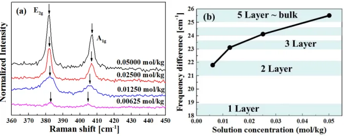
Figure 1(a) shows the Raman spectra for the MoS2 films fabricated by source solutions with various concentrations. Two Raman peaks, E2g and A1g, are observed in the Raman spectra for all films. The peak position difference, which is a good trace for the thickness estimation, is plotted in figure 1(b). The peak difference of the MoS2 film fabricated by the 0.05 mol/kg solution corresponds to a thickness of over five layers. On the other hand, a thickness of three layers was estimated for the film grown by the 0.0125 mol/kg solution. When the source solution with a concentration of 0.00625 mol/kg was used, the thickness of the film is further decreased to two mono-layers, although the Raman peak intensity becomes small.
The thin film transistors (TFT) using solution processed MoS2 as semiconductor which was directly deposited on the NZO as gate insulator, were fabricated with channel length of 10 µm and
width 50 µm, respectively as shown in figure 2(a). The 0.05 mol/kg MoS2 solution was used so the width of Raman peak in figure 2(a) was 26 cm-1 (over five layers). The calculated filed effect mobility which was calculated from figure 2(b), was 0.32~0.71 cm2/Vs. and the on/off ratio was 4.5x10⁴. This value is almost the same as that reported for TFT with transferred or CVD multilayer MoS2
Figure 1. (a) Raman spectra of MoS2 fabricated by source solutions with various concentrations. (b) Frequency difference between the peak of the E2g and A1g mode as a function of the concentration of the source solution.
Figure 2(a) Plan view of metal pad for multilayer MoS2 transistor and its Raman spectra, (b) the characteristic of (a)gate-voltage and drain current.
Reference
[1] K. Novoselov, “Graphene : Mind the gap”, Nature Material, vol.6, pp.720, 2007.
[2] A. Splendiani, L. Sun, Y. Zhang, T. Li, J. Kim, C. Chim, G. Galli and F. Wang, “Emerging Photoluminescence in Monolayer MoS2”, Nano letter, vol.10, pp.1271, 2010.
[3] B. Radisavljevic, A. Radenovic, J. Brivio, V. Giacometti &A. Kis, “Single-layer MoS2 transistors”, Nature nanotechnology, vol.6, pp.147, 2011.
[4] J. Putz and M. A. Aegerter, “Liquid Film Deposition of Chalcogenide Thin Films”, Journal of Sol-Gel Science and Technology, vol.26, pp.807, 2003.
Keywords: Solution process, High-k , MoS2, semiconductor, TFT