CREATED USING THE RSC ARTICLE TEMPLATE (VER. 3.0) - SEE WWW.RSC.ORG/ELECTRONICFILES FOR DETAILS
PAPER www.rsc.org/PCCP | Physical Chemistry Chemical Physics
a
Priority Organization for Innovation and Excellence, Kumamoto University, 2-39-1 Kurokami, Kumamoto 860-8555, Japan. Fax/Tel:
+81-96-342-3948; E-mail: [email protected]
b
Kumamoto Institute for Photo-Electro Organics (Phoenics), 3 – 11 – 38 Higashi-machi, Kumamoto 862 – 0901, Japan.
c
World Premier International Research Center, Advanced Institute for Materials Research (WPI-AIMR),Tohoku University, 2-1-1 Katahira, Aoba-ku, Sendai 980-8577, Japan, Fax/Tel: +81-22-217-5947; E-mail:
[email protected]
d
Fuel Cell Nanomaterials Center, University of Yamanashi, 6-43 Miyamae-cho, Kofu, Yamanashi 400-0021, Japan.
Potential-induced phase transition of low-index Au single crystal surfaces in propylene carbonate solution
Soichiro Yoshimoto,* a,b Youn-Geun Kim , c Kazuhiro Sato, c Junji Inukai d and Kingo Itaya* c
Received (in XXX, XXX) xxth October 2011, Accepted xxxxx 2011 First published on the web 1st xxxx 2011
5
DOI: 10.1039/c1cp00000x
In situ scanning tunneling microscopy (STM) was employed to examine the surface structures of Au(111), Au(100), and Au(110) single crystals in propylene carbonate (PC) containing tetrabutylammonium perchlorate (TBAP). All three electrodes exhibited potential-induced phase transition between the reconstructed and unreconstructed (1 ´ 1) structures at negative and positive
10
potentials, respectively. The potential-induced phase transition of the Au electrode surfaces is attributed to the interaction of TBA cation and perchlorate anion at the electrode surface , which is similar to that which takes place in aqueous solutions. In addition to static atomic structures, dynamic processes of both the reconstruction and the lifting of the reconstruction were investigated by means of in situ STM. The lifting of reconstructed Au(111)–( Ö 3 ´ 22) on Au(111) to the (1 ´ 1)
15
structure is completed within 1 min at a positive potential. The diffusion of Au atoms on Au(100) plane in the PC solution proceeds more rapidly than that in the aqueous solution, suggesting that the PC solvent plays an important role in accelerating the diffusion of Au atoms.
1. Intorduction
Scanning tunneling microscopy (STM) has provided detailed
20
information on atomic structures of electrified interfaces of metals and semiconductors in electrolyte solutions.
1Since the development of electrochemical STM (EC-STM) in 1988, EC- STM has been recognized as a powerful tool for the elucidation of solid/liquid interface at molecular and atomic
25
levels. In the past the majority of EC-STM studies have been performed in aqueous environment, dealing with atomic structures of reconstructed metal electrodes, adsorption of ionic species and molecules, and corrosion and electrodeposition at various metal and semiconductor
30
surfaces.
1–6In addition to studies made in aqueous solutions, many organic adlayers have been investigated in non-conductive organic solvents such as 1-phenyloctane and trichlorobenzene.
7–9EC-STM has also been applied to study
35
electrochemical reactions in non-aqueous polar solvents.
10–17Typical examples are the intercalation of lithium cations in the highly oriented pyrolytic graphite (HOPG),
10,11the deposition of lithium onto Au(111) in propylene carbonate (PC),
12the electrodeposition of several metals from ionic
40
liquids,
13–16the electrochemical annealing of Au(111) electrode in 3-methylimidazolium tetrafluoroborates,
17and the
epitaxial growth of polythiophene on iodine-modified Au(111) electrode in dichloromethane.
18,19The reconstruction of metal single crystal surfaces is one of the important
45
subjects in the electrochemical surface science for understanding electrode/electrolyte interfaces.
21The electrochemically induced reconstruction of Au single crystal electrodes has been extensively investigated in aqueous solutions using in situ STM by Kolb,
2,22Weaver and
50
Hamelin,
23–27and Magnuseen et al.
28–30The surface x-ray scattering method has also been applied to study this phenomenon by Ocko et al.
26It is well-known that the reconstructed structures such as Au(111)–( Ö 3 ´ 22), Au(100)–(5 ´ 20) (abbreviated as “hex”),
55
and Au(110)–(1 ´ 2) or Au(110)–(1 ´ 3) (the so-called
“missing rows” structure) are formed in negative potential regions. It is also known that such reconstructed structures are lifted to the (1 ´ 1) structure of each plane at more positive potentials with respect to their points of zero charge
60
(pzc).
2,20,21,31–36Although the reconstruction of the low- indexed gold single crystal surfaces has been extensively studied in aqueous solutions as described above, no STM invstigation has been reported for the reconstruction of gold electrodes in nonaqueous polar solvent.
65
In the present study, we observed reconstructed structures of the Au(111), (110), and (100) surfaces by using in situ STM in PC containing tetrabutylammonium perchlorate (TBAP). High resolution STM images of reconstructed surfaces were succesfully obtained by in situ STM for the first
70
time in dry nitrogen atmosphere. It is also reported that the reconstructed structures are transformed into the (1 ´ 1) unreconstructed structure for all low-index planes of Au in positive potential ranges. Time-dependent processes of both the reconstruction and the lifting of the reconstruction for all
75
low-index planes were also investigated.
2. Experimental
Single-crystal gold beads were prepared by melting the end of a pure Au wire (99.99%), followed by exposing Au(111), Au(100), and Au(110) surfaces by the mechanial polishing method described in the literature.
37The Au single crystal
5
electrodes were annealed in a hydrogen-oxygen flame and quenched in hydrogen-saturated Millipore water (resistivity >
18.2 M W ). Well-annealed single crystals were brought into an Ar glove box (Vacuum Atmospheres (VAC): HE-43-2), in which water and oxygen concentrations were kept below 1-2
10
ppm, and they were re-annealed in a small electrric furnace at ca. 950 ˚C. All electrochemical and STM measurements were performed in a high purity Ar atmosphere in a glove box system. Cyclic voltammetry was carried out at 20 ˚C using a potentiostat (HOKUTO HAB-151) with the hanging meniscus
15
method in a three-compartment electrochemical cell. In situ STM measurements were performed using a Nanoscope E (Digital Instruments) with a vibration isolator (VIC International: Nano-K). The tunneling tip was made of a tungsten wire (diameter 0.25 mm) prepared by
20
electrochemical etching in 1 M KOH. To minimize residual faradaic currents, the tips were coated with polyethylene (Aldrich). STM measurements were carried out directly on the facets of (111) and (100) formed on the single crystal bead as described previously.
38,39On the other hand, a
25
mechanically-polished (110) surface was used for STM studies, because (110) facets are absent on the surface of the single-crtstal bead. All STM images were acquired in the constant-current mode. A Pt wire was used as a quasi-
reference electrode in both the electrochemical and STM
30
measurements. All electrochemical potentials are reported with respect to ferrocene/ferrocenium reference electrode in PC.
3. Results and discussion
3.1 CV profiles.
35
First, cyclic voltammograms (CVs) of three low-index Au single crystal electrodes were measured in aqueous 0.1 M HClO
4. As seen in Fig. 1, panels a-c, all CV curves are almost identical in detail to those reported in several papers
22,34 40, indicating that well-defined surfaces were successfully
40
prepared in the present study. After confirming the quality of the Au single crystal electrodes, CV measurements were performed in a PC solution containing 0.1 M TBAClO
4in the Ar glove box as described in the experimental section.
In Fig. 1, panels d – f, wide double-layer potential regions
45
can be seen for all Au single crystal planes. For example, the CV in Fig. 1d obtained with the Au(111) electrode exibits a wide double layer potential range spanning from –2.80 V to 1.20 V. To obtain better understanding of the CV characteristics associated with structural changes of the
50
Au(111) surface, the CV shown by the dotted line was remeasured at the 20 times higher current sensitivity. The dotted CV curve in Fig. 1d suggests that a the pair of reversible peaks at approximately –0.50 V can be attributed to the reversible phase transition between the reconstructed and
55
the unreconstructed Au(111). As reported for aqueous
Fig. 1. Cyclic voltammograms of Au(111), Au(100), and Au(110) electrodes recorded at (a-c) 50 mV s
–1in
aqueous 0.1 M HClO
4, and at (d, e) 1 mV/s and (f) 5 mV/s in PC containing 0.1 M TBAClO
4. The dotted
traces are enlarged ( ´ 20) i-V profiles between 0.50 V and –2.50 V.
electrolyte solutions, the kinetics of lifting of reconstruction frequently depends on the anion of the electrolyte, where strongly adsorbed anions such as halide, sulfate, and sulfide accelerate the kinetics, while weakly adsorbed anions such as ClO
4–and PF
6–exhibit no effect.
405
The CV curves obtained at the Au(100) electrode (Fig. 1e) were similar to those at the Au(111) electrode. The dotted curve in Fig. 1e shows an enlarged i-V profile, in which some features ascribable to the phase transition of Au(100) can be seen, although the peaks are not clearly comparable with those
10
for Au(111). As reported in the literature,
40,41well-defined peaks due to phase transition are also absent for Au(100) in aqueous electrolyte solutions containing weakly adsorbed anions such as ClO
4–and PF
6–. It is postulated that the lifting of reconstructed Au(100)–(hex) is largely associated with the
15
adsorption of anions.
2,20,31–36CV curves on Au(110) are also similar to those on Au(100). The dotted line in Fig. 1f shows quasi-reversible peaks at approximately –0.8 V, which are likely to be due to the phase transition.
20
3.2 In situ STM imaging of Au(111) in PC.
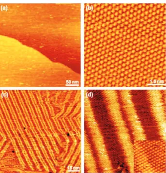
Panels a and b in Fig. 2 are, respectively, large-scale and high-resolution STM images obtained on the Au(111) electrode at –0.30 V, which is a potential more positive than the peak potential of –0.50 V seen in Fig. 1d. The imaging
25
was performed after 1 hr. The large-scale STM image shown in Fig. 2a reveals two atomically flat terraces separated by a monatomic step. The high-resolution STM image of Fig. 2b displays periodical corrugation heights with a hexagonal packing arrangement. This arrangement with an interatomic
30
spacing of 0.29 nm is in agreement with the Au(111)–(1 ´ 1) atomic structure. On the contrary, shifting the potential negatively from –0.30 to –1.50 V brought about the structure consisting of straight and irregularly-shaped lines on the terraces, as shown by the image (100 ´ 100 nm
2) in Fig. 2c.
35
The newly appeared lines are extended by more than 100 nm in the <112> direction. Higher-resolution STM scans were capable of discerning atomic features of the reconstructed Au(111) surface. An example of such close-up views is shown in Fig. 2d, in which two paired lines are separated by
40
approximately 2.1 nm, whereas two neighboring pairs are 6.7 nm apart. These characteristic patterns almost completely match those of the reconstructed Au(111)–( Ö 3 ´ 22) surface observed in UHV
32,42and aqueous electrolyte solutions.
2,5,20This reconstructed Au(111) surface emerged at ca. –0.50 V
45
and extended over the terrace when the electrode potential was scanned to more negative potentials. At ca. –1.5 V, the entire area of the atomically flat terrace was covered by the reconstructed structure after 1 hr.
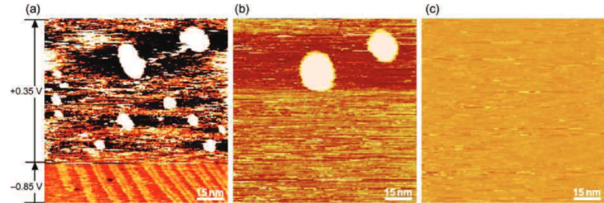
Figure 3a shows the dynamic process of lifting of the
50
reconstructed surface. When the electrode potential was abruptly changed from –0.85 to +0.35 V, the reconstructed surface appeared to be converted to the unreconstructed Au(111)–(1 ´ 1). The tunneling tip was scanning upward (Fig.
3a). Typical herringbone features seen at the lower portion of
55
the image disappeared immediately, producing islands with a monatomic height. The number of as-produced islands
accounted for about 4 % of the surface area, which resulted from aggregation of Au atoms ejected upon lifting of the reconstruction.
2,20The subsequent evolution of the Au(111)
60
surface is revealed by the time-dependent STM images of panels b and c in Fig. 3 taken, respectively, 30 and 60 s after Fig. 3a was recorded. Only two disk-shaped islands were left with diameters that are twice or three times those seen in Fig.
3a, suggesting the occurrence of rapid diffusion of gold atoms
65
and entrapment into larger Au islands. These two islands existed only temporarily as they were no longer present in the STM image shown in Fig. 3c. Note that the surface diffusion of Au atoms in a pure aqueous solution of HClO
4is relatively slow, although it is known that the presence of adsorbed
70
chloride enhances the mobility. It is remarkable that the surface diffusion of Au in PC is much faster that that in aqueous solutions.
43,44The surface structure of Au(111) is expected to be reconstructed and unreconstructed, respectively, at potentials
75
negative and positive of the pzc in acidic solutions.
2,20,22,31-36The present STM results suggest that the pzc of the Au(111) electrode in PC is either at or near –0.5 V, as this is the potential where the reconstructed (Ö3 ´ 22) and (1 ´ 1) structures were inter-converted. Such experimental results
80
suggest that the surface charges play an important role for the reconstruaction of Au(111).
31–363.3 In situ STM imaging of Au(100) in PC.
Fig. 2. Large-scale STM and high-resolution topographies of Au(111)
surface obtained at –0.30 V for panels (a) and (b) and at –1.50 V for
panels (c) and (d). High-resolution STM scan (d) shows details of the
herringbone structures on an atomically-flat terrace. The dimensions of
these features are as indicated. The inset in (d) shows the atomic
structure of reconstructed Au(111) surface. Tip potential and tunneling
current were 0.20 V and 5.0 nA, respectively.
STM images a and b in Fig. 4 were obtained with an Au(100) electrode at –1.80 V in PC. The large-scale image in Fig. 4a reveals an elongated strand pattern aligned along either [011] or [ 0 1 1 ] direction as marked by the arrow signs.
The atomic-resolution STM image in Fig. 4b was obtained on
5
an atomically flat terrace, and it reveals a pseudo hexagonal structure with an interatomic spacing of 0.29 nm. Each Au atom can be clearly seen in this high-resolution STM image.
These STM images are consistent with those reported for the
“hex” phase of the reconstructed Au(100) surface in UHV
4510
and in aqueous solutions.
27,28After acqusition of the images a and b in Fig. 4, the electrode potential was scanned in the positive direction from –1.80 to 0.30 V, which resulted in the very different STM images shown in Figs. 4c and 4d. Smooth wide terraces and
15
protruded islands are seen over the surface. The breath of the terrace seen in Fig. 4c spans nearly 300 nm, and all islands are raised by 0.25 nm with respect to the wide terrace. Zooming onto the terrace yielded an atomic-resolution STM image of Fig. 4d, which shows a square array with the nearest neighbor
20
spacing of 0.29 nm. The atomic rows are almost perfectly aligned along the [011] or [ 011 ] direction. Thus, it is concluded that the “hex” phase is converted to the Au(100)–(1
´ 1) lattice at 0.30 V in PC.
According to the previous reports on the phase transition of
25
Au(111) and Au(100) electrodes in aqueous electrolytes,the pzc’s of the reconstructed Au(111) and Au(100) electrodes are 0.32 and 0.30 V (vs. saturated calomel electrode: SCE) in 0.01 M HClO
4, respectively.
18It is believed that the pzc’s of these electrodes would not differ substantially even in PC, although
30
the CV of Au(100) exhibited broad peaks in PC as shown in Fig. 1e.
Figure 5 shows the dynamic process of lifting of the reconstructed surface. As can be seen in Fig. 5a, relatively flat terraces with islands and pits with the monatomic height
35
were consistently observed at –2.0 V. Some pits are marked by white arrows. After the potential was stepped to 0.30 V from –2.0 V in the third-quarter portion of the image, small patches began to appear at the well-defined striped arrays, as can be seen in the lower portion of the image. Fig. 5b was
40
obtained at the same location as for Fig. 5a. The image in Fig.
5b was obtained in the next scan performed 25 s after that of
Fig. 5a was recorded. Small Au islands, ca. 2 to 4 nm in diameter, appeared not only on the terrace but also on the monatomic island in the upper portion of the image. In
45
general, the (1 ´ 1) surface contained a high density of islands resulting from the 24 % difference in the density of surface Au atoms between these two phases.
2,27,28The excess Au atoms formed monatomic Au islands on the (1 ´ 1) terrace, which resulted from the lifting of the reconstruction. Gao et al.
50
reported that islands measuring 2 to 4 nm in diameter were also found at the initial stages of island formation on Au(100) in HClO
4.
29A remarkable structural change was found near Fig. 3. (a) Composite STM scans showing the effect of potential on the surface structure of Au(111). The potential of
Au(111) electrode was stepped from –0.85 to +0.35 V as the tip was moved upward to one-third of the frame. Panels (b) and (c) were taken, respectively, 30 s and 60 s after panel (a) was recorded.
Fig. 4. Large-scale and high-resolution STM images showing the
reconstructed Au(100) surface obtained at –1.50 V for panels (a) and
(b) and at 0.30 V for panels (c) and (d). Tip potential and tunneling
current were 0.2 V and 5.0 nA, respectively. The sets of two arrows
indicate atomic rows in the <110> direction.
the step of the monatomic island. Fig. 5c shows an STM image taken after 1 min, exhibiting terraces with the monatomic island. The entire surface is seen to be covered by monatomic Au islands. The size of each Au island in this image was as large as 5-8 nm. The pit indicated by the white
5
arrow sign in Fig. 5b became much smaller. The STM image of Fig. 5d taken 1 min after that of Fig. 5c was recorded, indicates that the size of Au islands became larger than those in Fig. 5c. The size of those Au islands was typically 8 nm to 15 nm in diameter. The pit pointed at by the white arrow sign
10
became much smaller. Although the diffusion rate of Au atom on Au(100) is reported to be slower than that on Au(111) in aqueous solution,
46the diffusion of Au atoms on Au(100) in PC seems to be more rapid than that in aqueous solutions. A more detailed study of this aspect is in progress.
15
3.4 In situ STM imaging of Au(110) in PC.
Fig. 6 shows the STM results obtained with a mechanically exposed Au(110) electrode at 0.3 V. The large-scale and high-resolution STM images of panels a and b in Fig. 6 were
20
recorded at 0.30 V, which reveal well-defined terraces and monatomic steps (∆Z = 0.23 nm). The average terrace width is ca. 20 nm, which is smaller than that on Au(111) or Au(100) facet. However, the atomic structure seen in Fig. 6b appears to be rectangular with the close-packed atomic rows
25
aligned along the [ 110 ] direction. The interatomic spacings of 0.29 and 0.40 nm were measured along the [ 110 ] and [001]
directions, respectively. The image shown in Fig. 6b indicates that the Au(110) surface has the (1 ´ 1) structure at 0.30 V.
These two directions correspond to those of an ideal Au(110)–
30
(1 ´ 1) structure. The same atomic structure has been reported in 0.1 M HClO
4, as described in our previous paper.
47Step ledges are roughly aligned along the [001] direction, which apparently caused the formation of unfavorable, open atomic structures, leading to the rugged step ledges seen in
35
Fig. 6b.
Switching the potential from 0.30 to –1.50 V yielded the STM images in Fig. 7. The first image in Fig. 7a, acquired as a result of an upward scan, reveals drastically different surface morphologies of the Au(110) electrode at 0.30 V
40
(lower half) and at –1.50 V (upper half). Well-defined terrace and step features similar to those of Fig. 6a were seen at 0.30 V, but severe roughening was noted at –1.50 V. It seems that upon stepping the potential, well-defined terraces formed at 0.30 V were immediately sliced into elongated stripes in
45
parallel to the [ 110 ] direction. Upon waiting, the surface evolved into broken terraces with extended fingers stretching from step ledges only along the [ 110 ] direction. The formation of this reconstructed structure can be attributed to the efficient mass transfer along the [ 110 ] direction. These
50
finger-like features were observed for Au(110) and Ag(110) at Fig. 6. (a) In situ STM topographic scan of Au(110)–(1 ´ 1) obtained at 0.30 V. (b) High resolution STM scan showing the atomic structure of Au(110) at 0.30 V. Tip potential and tunneling current were 0.2 V and 5.0 nA, respectively.
Fig. 5. Time-dependent STM images (100 ´ 100 nm
2) showing the potential-induced lifting process of the reconstructed Au(100) surface in PC containing 0.1 M TBAClO
4obtained at 0.30 V upon stepping the potential from –2.00 V. Panels (b), (c) and (d) were taken, respectively, 25 s, 60 s and 120 s after panel (a) was recorded. Tip potential and tunneling current were 0.3 V and 5.0 nA, respectively.
Fig. 7. (a) Composite STM scans showing the effect of potential on the
surface structure of Au(110). The potential of Au(110) was stepped
from 0.30 to –1.50 V as the tip was moved upward to one-third of the
frame. (b) In situ STM topographic scan recorded 30 s after the
potential step.
high temperatures in UHV.
48The characteristic surface morphology of the terrace is closely associtated with the reconstructed (1 ´ 2) structure, because a similar reconstructed sruface showing (1 ´ 2) structure can be seen in 0.1 M HClO
4. Unfortunately, however, higher resolution
5
STM images of the reconstructed (1 ´ 2) structure could not be obtained in PC under the present experimental conditions, whereas a clear STM image of reconstructed (1 ´ 2) structure was observed in 0.1 M HClO
4. As described in the previous section, the diffusion rate (or mobility) of Au atoms on the
10
unreconstructed surface in PC solution is much higher than that in aqueous solution. Therefore, the exchange reaction of Au atoms between the terrace and the step can easily occur on the Au(110) surface in PC. It should be noted that the reconstructed structure of Au(110) depends on the cations
15
present in the solution. For example, the (1 ´ 3) reconstruction is favored when the solution contains alkali cations such as Na
+and K
+, whereas the (1 ´ 2) structure is produced in the presence of protons.
49Thus far, we have not seen the (1 ´ 3) reconstruction, which has been suggested to
20
be more favorable than the (1 ´ 2) structure.
504. Conclusions
We succeeded in in situ STM imaging of clean Au(111), Au(100), and Au(110) electrode surfaces in nonaqueous PC solution under electrochemical conditions. In situ STM
25
revealed that the surfaces of negatively-charged Au(111), Au(100), and Au(110) electrodes in PC are similar to those observed in aqueous electrolytes, and they assumed reconstructed structures of ( Ö 3 ´ 22), “hex”, and (1 ´ 2), respectively. Shifting the potential in the positive direction
30
beyond their pzc’s causes lifting of the reconstruction to the (1 ´ 1) structure. Because both cations and anions interact only weakly with these gold electrodes, the adsorption of anionic species is not responsible for the STM results. Rather, the electrostatic effect that dominates the charges at gold
35
electrodes drives these structural changes.
31–36The lifting of reconstruction of gold surfaces results in the ejection of gold atoms on the surfaces, and they diffuse rapidly and form aggregates upon collision. In the case of Au(110), gold atoms diffuse preferentially along the [ 110 ] direction, yielding
40
elongated fingers protruding from the steps. Finally, electrochemical STM investigations at nonaqueous electrochemical interfaces are expected to elucidate not only the dynamics of adsorption, organization and growth for various organic compounds including metal-organic
45
complexes, but also electrochemical reactions with radical cations and anions at atomic and molecular scales.
Acknowledgment
This work was supported in part by the Core Research for Evolutional Science and Technology (CREST) of the Japan
50
Science and Technology Agency (JST), and by a Grant-in-Aid for Young Scientists (A) (No. 21681012) and Scientific Research on Innovative Areas No. 21108005, "Coordination Programming" from MEXT, Japan. The authors acknowledge Dr. Y. Okinaka for his assistance in writing this manuscript.
55
Notes and references
a
, Priority Organization for Innovation and Excellence, Kumamoto University, 2-39-1 Kurokami, Kumamoto 860-8555, Japan. Fax/Tel:
+81-96-342-3948; E-mail: [email protected]
b
Kumamoto Institute for Photo-Electro Organics (Phoenics), 3 – 11 – 38
60
Higashi-machi, Kumamoto 862 – 0901, Japan.
c
World Premier International Research Center, Advanced Institute for Materials Research (WPI-AIMR), Tohoku University, 2-1-1 Katahira, Aobaku, Sendai 980-8577, Japan, Fax/Tel: +81-22-217-5974; E-mail:
[email protected]
65
d
Fuel Cell Nanomaterials Center, University of Yamanashi, 6-43 Miyamae-cho, Kofu, Yamanashi 400-0021, Japan.
† Electronic Supplementary Information (ESI) available: [details of any supplementary information available should be included here]. See DOI: 10.1039/c1cp00000x/
70
‡ Footnotes should appear here. These might include comments relevant to but not central to the matter under discussion, limited experimental and spectral data, and crystallographic data.
1 K. Itaya, Prog. Surf. Sci., 1998, 58, 121.
75
2 D. M. Kolb, Prog. Surf. Sci., 1996, 51, 109.
3 A. A. Gewirth and B. K. Niece, Chem. Rev., 1997, 97, 1129.
4 O. M. Magnussen, Chem. Rev., 2002, 102, 679.
5 M. J. Weaver and X.-P. Gao, Annu. Rev. Plrys. Chern., 1993, 44, 459.
2 S. Ye, T. Kondo, N. Hoshi, J. Inukai, S. Yoshimoto, M. Osawa and K.
80
Itaya, Electrochemistry, 2009, 77, 2.
3 S. De Feyter and F. C. De Schryver, Self-assembly at the liquid/solid interface: STM reveals. J. Phys. Chem. B, 2005, 109, 4290.
4 M. Lackinger, S. Griessl, W. M. Heckl, M. Hietschold and G. W. Flynn, Langmuir, 2005, 21, 4984.
85
5 J. A. A. W. Elemans, I. De Cat, H. Xu and S. De Feyter, Chem. Soc.
Rev., 2009, 38, 722.
6 M. Inaba, Y. Kawatate, A. Funabiki, S.-K. Jeong, T. Abe and Z. Ogumi, Electrochim. Acta, 1999, 45, 99.
7 T. Doi, M. Inaba, Y. Iriyama, T. Abe and Z. Ogumi, J. Electrochem.
90
Soc., 2008, 155, A20.
8 T. Saito and K. Uosaki, J. Electrochem. Soc., 2003, 150, A532.
9 C. A. Zell, F. Endres and W. Freyland, Phys. Chem. Chem. Phys., 1999, 1, 697.
10 D. Borissov, C. L. Aravinda and W. Freyland, J. Phys. Chem. B, 2005,
95
109, 11606.
11 G.-B. Pan and W. Freyland, Chem. Phys. Lett., 2006, 427, 96.
12 Y.-C. Fu, J.-W. Yan, Y. Wang, J.-H. Tian, H.-M. Zhang, Z.-X. Xie and B.-W. Mao, J. Phys. Chem. C, 2007, 111, 10467.
13 L.-G. Lin, Y. Wang, J.-W. Yan, Y.-Z. Yuan, J. Xiang and B.-W. Mao,
100
Electrochem. Commun., 2003, 5, 995.
14 H. Sakaguchi, H. Matsumura and H. Gong, Nature Mater., 2004, 3, 551.
15 H. Sakaguchi, H. Matsumura, H. Gong and A. M. Abouelwafa, Science, 2005, 310, 1002.
105
16 Interfacial Electrochemistry; A. Wieckowski, Ed.; MARCEL DEKKER, Inc: New York, 1999.
17 Structure of Electrified Interfaces; J. Lipkowski and P. N. Ross, Eds.;
WILEY–VCH: New York, 1993.
18 D. M. Kolb and J. Schneider, Electrochim. Acta, 1986, 31, 929.
110
19 X.-P. Gao, A. Hamelin and M. J. Weaver, Phys. Rev. B, 1991, 44, 10983.
20 X. P. Gao, A. Hamelin and M. J. Weaver, Phys. Rev. Lett., 1991, 67, 618.
21 A. Hamelin, J. Electroanal. Chem., 1992, 329, 247.
115
22 B. M. Ocko, G. Helgesen, B. Schardt, J. Wang, and A. Hamelin, Phys.
Rev. Lett., 1992, 69, 3350.
23 X. Gao, G. J. Edens, A. Hamelin and M. J. Weaver, Surf. Sci., 1993, 296, 333.
24 O. M. Magnussen, J. Hotlos, R. J. Behm, N. Batina and D. M. Kolb,
120
Surf. Sci., 1993, 296, 310.
25 M. Labayen, C. Ramirez, W. Schattke and O. M. Magnussen, Nature Mater., 2003, 2, 783.
26 T. Tansel and O. M. Magnussen, Phys. Rev. Lett., 2006, 96, 026101(- 1)–026101(-4).
125
31 V. Fiorentini, M. Methfessel and M. Scheffler, Phys. Rev. Lett., 1993, 71, 1051.
32 J. V. Barth, H. Brune, G. Ertl and R. J. Behm, Phys. Rev. B, 1990, 42, 9307.
33 H. Ibach, C. E. Bach, M. Giesen and A. Grossman, Surf. Sci., 1997,
5
375, 107.
34 E. Santos and W. Schmickler, Chem. Phys. Lett., 2004, 400, 26.
35 J. Wang, A. J. Davenport, H. S. Isaacs and B. M. Ocko, Science 1992, 255, 1416.
36 C. Vaz-Domínguez, A. Aranzabal and A. Cuesta, J. Phys. Chem. Lett.
10
2010, 1, 2059.
37 J. Clavilier, R. Faure, G. Guinet and R. Durand, J. Electroanal. Chem., 1980, 107, 205.
38 J. Schneir, R. Sonnenfeld, O. Marti, P. K. Hansma, J. E. Demuth and R.
J. Hamers, J. Appl. Phys., 1988, 63, 717.
15
39 K. Itaya, S. Sugawara, K. Sashikata and N. Furuya, J. Vac. Sci.
Technol. A, 1990, 8, 515.
40 A. Hamelin, J. Electroanal. Chem., 1996, 407, 1.
41 A. Hamelin and L. Stoicoviciu, J. Electroanal. Chem., 1987, 234, 93.
42 Ch. Wöll, S. Chiang, R. J. Wilson and P. H. Lippel, Phys. Rev. B, 1989,
20
39, 7988.
43 J. D. Trevor, C. E. D. Chidsey and D. N. Loiacono, Phys. Rev.
Lett.,1989, 62, 929.
44 H. Honbo, S. Sugawara and K. Itaya, Anal. Chem., 1990, 62, 2424.
45 Y. Kuk and P. J. Silverman, Appl. Phys. Lett., 1986, 48, 1597.
25
46 M. Hara, Y. Nagahara, J. Inukai, S. Yoshimoto and K. Itaya, Electrochim. Acta, 2006, 51, 2327.
47 H. Honbo and K. Itaya, J. Chim. Phys., 1991, 88, 1477.
48 R. Koch, M. Sturmat and J. J. Schulz, Surf. Sci., 2000, 454-456, 543.
49 J. X. Wang, G. M. Watson and B. M. Ocko, J. Phys. Chem., 1996, 100,
30