Japan Advanced Institute of Science and Technology
https://dspace.jaist.ac.jp/
Title
Formation of silicon-fullerene-linked nanowires
inside carbon nanotubes: A molecular-dynamics and
first-principles study
Author(s)
Nishio, Kengo; Ozaki, Taisuke; Morishita,
Tetsuya; Mikami, Masuhiro
Citation
Physical Review B, 77(20): 201401-1-201401-4
Issue Date
2008-05-12
Type
Journal Article
Text version
publisher
URL
http://hdl.handle.net/10119/10841
Rights
Kengo Nishio, Taisuke Ozaki, Tetsuya Morishita,
and Masuhiro Mikami, Physical Review B, 77(20),
2008, 201401. Copyright 2008 by the American
Physical Society.
http://dx.doi.org/10.1103/PhysRevB.77.201401
Description
Formation of silicon-fullerene-linked nanowires inside carbon nanotubes:
A molecular-dynamics and first-principles study
Kengo Nishio,1,
*
Taisuke Ozaki,2 Tetsuya Morishita,1and Masuhiro Mikami11Research Institute for Computational Sciences (RICS), National Institute of Advanced Industrial Science and Technology (AIST), Central 2, Umezono 1-1-1, Tsukuba, Ibaraki 305-8568, Japan
2Research Center for Integrated Science (RCIS), Japan Advanced Institute of Science and Technology (JAIST), 1-1 Asahidai, Nomi, Ishikawa 923-1292 Japan
共Received 13 March 2008; published 12 May 2008兲
We study the formation of Si nanowires inside carbon nanotubes by using a combination of empirical molecular-dynamics and first-principles approaches. Molecular-dynamics simulations demonstrate that liquid Si encapsulated into a共13,0兲 nanotube crystallizes into a nanowire composed of linked Si16fullerene cages. On the other hand, a nanowire composed of linked Si20 fullerene cages forms inside a 共14,0兲 nanotube. The
stabilities of these nanowires are further confirmed by first-principles calculations. We also find that the freestanding Si16-linked nanowire is a metal, while the Si20-linked nanowire is a semiconductor. The present
findings suggest that the choice of the nanotube size allows us to control the structure of Si nanowires, and therefore to tailor the material properties.
DOI:10.1103/PhysRevB.77.201401 PACS number共s兲: 61.48.⫺c, 62.23.Hj, 73.22.⫺f, 73.61.Wp
Si nanowires共Si NWs兲 have attracted much attention be-cause of their potential uses in future nanoscale devices.1–12
The electronic and optical properties of Si NWs are consid-erably different from those of bulk Si and dramatically de-pend on the wire diameter and atomic structure.4,5,7 The
stable atomic structure also depends on the wire diameter. Recent theoretical predictions indicate that Si NWs could have atomic structures not seen in the bulk Si.3–5,9,10,12These
significant features lead to the idea of tailoring the properties of Si NWs for specific applications through the size and structure.
The use of nanoporous materials as templates is a power-ful way of synthesizing nanomaterials in a controlled man-ner. The size and structure are determined by how the con-stituent atoms fit the interior space of nanopores. The usefulness of the template method has been demonstrated in various systems.3,5,13–18Even a single atomic chain, which is
the ultimate nanowire, has been synthesized for gadolinium18
and iodine17 by using a carbon nanotube 共CNT兲 as a
tem-plate. Recent molecular-dynamics 共MD兲 simulations have demonstrated that nonbulklike Si NWs, such as
stacked-polygon nanotubes with diameters ranging from
0.34 to 0.48 nm共Ref. 5兲 and a polyicosahedral nanowire of
1.30 nm in diameter,3are formed by freezing liquid Si inside
cylindrical nanopores. Here, the wire diameter is defined as the diameter of the smallest cylinder that contains the nano-wire. In these MD studies, nanopores were assumed to be a chemically inert container for liquid Si and modeled by ex-ternal potentials, which restrict the motion of Si atoms to cylindrical nanospaces. However, it is not clear whether such nanopores really exist.
We expect that CNTs can serve as such containers for the following reasons. First, silicon does not react with the sur-face of graphite.6Therefore, the wall of CNTs is expected to be inert to chemical reactions with silicon. Second, CNTs have high thermal stability. Actually, CNTs of 1.46 nm in diameter stood during heat treatment at 1873 K,19which is a
considerably high temperature compared to the melting tem-perature of bulk Si共1685 K兲. Furthermore, the wall of CNTs
was shown to be inert to chemical reactions with liquid Ge.20
These all support the idea of exploiting CNTs as templates for Si NWs.
In this Rapid Communication, we demonstrate by using a combination of empirical MD and first-principles approaches the formation of Si NWs by freezing liquid Si inside CNTs. A nanowire composed of linked Si16 fullerene cages forms
inside a 共13,0兲 CNT of 1.03 nm in diameter. On the other hand, a nanowire composed of linked Si20 fullerene cages
appears inside a 共14,0兲 CNT of 1.11 nm in diameter. The Si16- and Si20-linked NWs with diameters of 0.53 and
0.61 nm, respectively, are larger than the stacked-polygon nanotubes and smaller than the polyicosahedral nanowire. The stabilities of Si-fullerene-linked NWs are further con-firmed by the density functional theory 共DFT兲 within the local density approximation共LDA兲.21–24We also find that the
freestanding Si16-linked NW is a metal, while the Si20-linked
NW is a semiconductor.
In our MD simulations, Si and C atoms were modeled by the Tersoff potential.25The Tersoff potential is known to pro-vide an accurate description of covalent bonds in many forms of silicon, silicon carbide, and carbon,25,26 which is
necessary to simulate a multicomponent system comprised of a Si NW and a CNT. Our previous study of Si nanosheets inside slit pores showed that the Tersoff MD simulations and first-principles MD simulations yield essentially the same results,27 suggesting that the result obtained by using the
Tersoff potential is a good starting point for further sophisti-cated calculations.
Liquid Si consisting of 52 Si atoms was first prepared inside a共13,0兲 CNT consisting of 624 C atoms. Free bound-ary conditions were used for the system. The system was equilibrated at 2400 K 共1.02Tm兲 by using Nosé–Poincaré
thermostat.28,29 Here, Tm共2350 K兲 is the melting point
esti-mated for bulk Si by using the Tersoff potential. Although the CNT was partly distorted due to the thermal motion of C atoms, the overall structure stood at 2400 K. The system was then annealed at 1800 K 共0.77Tm兲 for 15 ns. Figure 1共a兲
atoms averaged over 0.2 ns. The energy abruptly drops around 10 ns, which signifies the phase transformation of the encapsulated Si. Figure 1共b兲 demonstrates that the encapsu-lated liquid Si crystallizes into a nanowire constructed by linking four Si16 fullerene cages with D4vsymmetry. All the
Si atoms in the nanowire are joined by tetrahedral bonding. The constituent Si16 cage has two square faces and eight
pentagonal faces. The square faces face each other. Adjacent Si16 cages are linked together by sharing one square face.
The fourfold symmetry axes of the Si16cages coincide with
the axis of the nanowire. We note that the Si16-linked NW has no corresponding bulk structure in a sense that it cannot be made by cutting out any crystalline phases of bulk Si.
Similar MD simulations were performed for a system of 65 Si atoms encapsulated into a 共14,0兲 CNT consisting of 672 C atoms关Figs.1共a兲and1共c兲兴. In contrast to the system of Si52@关共13,0兲 CNT兴, the Si16-linked NW is not observed inside the 共14,0兲 CNT. Instead, a nanowire constructed by linking four Si20fullerene cages with D5vsymmetry appears.
All the Si atoms in the nanowire are joined by tetrahedral bonding. The constituent Si20 cage has 12 pentagonal faces.
Adjacent Si20 cages are linked together by sharing one
pen-tagonal face. The fivefold symmetry axes of the Si20 cages
coincide with the axis of the nanowire. We note that the Si20-linked NW is a fragment of the framework of type-II Si clathrates.6–8In the bulk system, almost guest-free type-II Si
clathrates are synthesized from guest-encapsulated ones by removing guest atoms.30
In order to clarify how the chirality of CNT and the num-ber of Si atoms affect the structure of encapsulated Si NWs, we performed similar MD simulations for 120 Si atoms en-capsulated into 共10,4兲 and 共12,4兲 CNTs. The diameters of 共10,4兲 and 共12,4兲 CNTs, which are 0.99 and 1.15 nm, are comparable to the diameters of共13,0兲 and 共14,0兲 CNTs, re-spectively. The Si16-linked NW formed inside the 共10,4兲
CNT, while the Si20-linked NW appeared inside the 共12,4兲
CNT. These results indicate that the CNT diameter is the most important factor in determining the structure of encap-sulated Si NWs.
The geometrical constraint alters the relative stability of Si-fullerene-linked NWs. The freestanding infinite
Si20-linked NW is energetically more stable by
0.102 eV/atom than the Si16-linked NW. This is because the former contains pentagonal faces only, while the latter con-tains square and pentagonal faces.1,31The interior angle of a
pentagon, which is 112°, is close to the ideal bond angle in tetrahedrally bonded structures, which is 109.47°. On the contrary, the angle of a square, which is 90°, deviates from the ideal angle. Therefore, the tetrahedrally bonded structure prefers pentagonal faces to square faces. The Si20-linked NW
fits the hollow space of the共14,0兲 CNT. However, the space of the 共13,0兲 CNT is too narrow for the Si20-linked NW.
Therefore, the thinner Si16-linked NW forms inside the
共13,0兲 CNT.
We further examined the stabilities of Si-fullerene-linked NWs inside CNTs by using the DFT within the LDA. In our DFT calculations, norm-conserving pseudopotentials were used in a separable form with multiple projectors to replace the deep core potential into a shallow potential.32,33 The
wave functions were expressed by the linear combination of atomic orbitals centered on atomic sites. The atomic basis functions were generated by solving atomic Kohn–Sham equations by using confinement pseudopotentials.34,35 The
primitive pseudoatomic basis set,共Si6.5-s2p2d1兲, was used for Si, where the abbreviation Si6.5-s2p2d1 represents the employment of two primitive s orbitals, two primitive p or-bitals, and one primitive d orbital of a Si atom, which were generated with a confinement radius of 6.5 bohr. The con-tracted pseudoatomic basis set, C4.5-s31p31, was used for C atoms, where s31 represents that one s orbital was generated by contracting three primitive s orbitals of a C atom. The contraction coefficients were optimized to minimize the total energy of a共13,0兲 CNT. The contracted bases improve the accuracy of the calculation without increasing the computa-tional cost.35The real space grid techniques were used with
the cutoff energy of about 120 Ry when calculating Hamil-tonian matrix elements and solving the Poisson equation with a fast Fourier transformation.36All the DFT calculations
were carried out by using the OpenMXcode.37
To decrease the computational cost, we extracted systems of Si52@C416and Si65@C448from the systems obtained from
the Tersoff MD simulations of Si52@C624 and Si65@C672, respectively. These systems were then relaxed by an eigen-vector following method38 until the force on each atom
be-comes below 0.0003 and 0.0008 hartree/bohr for Si52@C416
and Si65@C448, respectively. Figures 2共a兲 and 2共d兲 show
the optimized structures of Si52@关共13,0兲 CNT兴 and Si65@关共14,0兲 CNT兴, respectively. No significant change is
FIG. 1.共Color online兲 共a兲 Time evolution of the interaction en-ergy of Si atoms for Si52@关共13,0兲 CNT兴 共solid line兲 and
Si65@关共14,0兲 CNT兴 共dashed line兲. Snapshots of the atomic
con-figurations corresponding to the filled and open circles are given in 共b兲 and 共c兲.
NISHIO et al. PHYSICAL REVIEW B 77, 201401共R兲 共2008兲
observed in the overall Si-fullerene-linked structures except for local changes at the wire tips. The DFT calculations thus provide convincing evidence that Si-fullerene-linked NWs are stable inside CNTs.
The isosurface maps of electron density for
Si52@关共13,0兲 CNT兴 关Fig. 2共b兲兴 and Si65@关共14,0兲 CNT兴
关Fig.2共e兲兴 show that no covalent bond is formed between a Si NW and a CNT. This confirms the chemical inertness of CNT. We also find that C atoms are joined by sp2 covalent bonding. Actually, electrons are localized along the lines joining each atoms. Figures2共c兲and2共f兲show that Si atoms apart from the wire tips are joined by sp3 covalent bonding.
The covalency in the bonds between the tip Si atoms is low-ered. Actually, electrons are somewhat delocalized over the tip Si atoms. This delocalized nature of electrons is due to the rearrangement of Si atoms caused by coordination de-fects. The DFT calculations provide an accurate description of the tip structure, which the Tersoff potential fails because of the delocalized bonding.
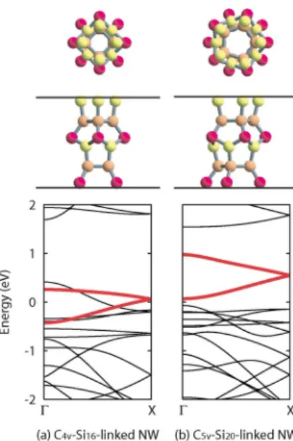
We further investigated the stabilities of Si-fullerene-linked NWs against the local cage distortion by using the DFT calculations. Calculations were performed for free-standing infinite nanowires because the关Si NW兴@CNT com-posite systems are too large to tackle several possible con-figurations. The periodic boundary condition was applied along the wire axis. The unit cells of Si16- and Si20-linked
NWs contain 24 and 30 Si atoms, respectively. Seven and five k-point samplings were used. Our DFT calculations re-vealed that the nanowires composed of lower-symmetry C4v-Si16 and C5v-Si20 cages are energetically more stable
than the nanowires composed of D4v-Si16and D5v-Si20cages,
respectively. The total energies of C4v-Si16-, D4v-Si16-, C5v-Si20-, and D5v-Si20-linked NWs are −3.9771, −3.9750,
−3.9798, and −3.9754 hartree/atom, respectively. The higher stability of the lower-symmetry nanowires is attributed to the local atomic configurations, which resemble that of a stable Si共111兲2⫻1 surface with buckled -bonded chains.39 All
the Si atoms in the higher-symmetry nanowires are joined by three-dimensional sp3bonding, and 16 and 20 atoms per unit cell have one dangling bond in the D4v-Si16- and
D5v-Si20-linked NWs, respectively. These threefold coordi-nated atoms are rearranged in the lower-symmetry nanowires 关Figs.3共a兲and3共b兲兴 to form -bonded chainlike structures, which resemble the reconstructed Si共111兲2⫻1 surface. Ac-tually, the light gray 共yellow兲 atoms are joined by planer sp2-like bonding and correspond to atom 11 in Ref.39, and
the outermost dark gray共red兲 atoms correspond to atom 12. The dangling bond energy is lowered by the formation of the -bonded chainlike structure as in the case of the bulk sur-face. This explains why the lower-symmetry nanowires are
FIG. 2. 共Color online兲 共a兲 Structure of Si52@关共13,0兲 CNT兴
optimized by using the DFT calculations. 共b兲 Isosurface 共0.05 electrons/bohr3兲 of the electron density for Si
52@关共13,0兲 CNT兴
共Ref.42兲. 共c兲 Isosurface 共0.035 electrons/bohr3兲 near the Si atoms.
Results for Si65@关共14,0兲 CNT兴 are given in 共d兲–共f兲.
FIG. 3.共Color online兲 Electronic band structures of 共a兲 C4v-Si16
-and共b兲 C5v-Si20-linked NWs. Energy is measured from the Fermi energy. Bands drawn in bold 共red兲 lines are the bands of sp2 bonded Si atoms. The unit cell of the nanowires is depicted in the upper parts. The vertical lines represent the optimized lengths of the unit cell, which are 1.048 nm共C4v-Si16-linked NW兲 and 1.068 nm
共C5v-Si20-linked NW兲. The light gray 共yellow兲 atoms are joined by sp2-like bonds. The other atoms, which are the gray共orange兲 and
energetically more stable than the higher-symmetry nano-wires. Note that when all the dangling bonds are terminated by hydrogen atoms, the reconstructed structure becomes un-stable, and the hydrogen-terminated lower-symmetry nano-wires transform to the higher-symmetry nanonano-wires with ideal sp3 bonds. The higher-symmetry structures might be stabi-lized by encapsulating guest atoms into fullerene cages as well.40,41
Figures3共a兲and3共b兲 show the electronic band structures of lower-energy C4v-Si16- and C5v-Si20-linked NWs,
respec-tively. Interestingly, the electronic structures are utterly dif-ferent. The C4v-Si16-linked NW is a metal. On the other
hand, the C5v-Si20-linked NW is a direct-band-gap semicon-ductor with a 0.14 eV band gap. This result is consistent with previous studies of the Si20-linked NW.7,8The calculation of
the radiative recombination rate revealed that the optical di-pole transition between the lowest unoccupied and highest occupied molecular orbitals is prohibited, even though the C5v-Si20-linked NW is a direct-band-gap semiconductor. The
position of theband closely relates to the electronic prop-erties. Theband of the metallic C4v-Si16-linked NW
over-laps with other bands. On the other hand, in the semicon-ducting C5v-Si20-linked NW, the band is separated from
the other bands. We note that the hydrogen-terminated nano-wires are semiconductor because dangling bond states are swept out from the fundamental gap region.
In summary, we have demonstrated that liquid Si encap-sulated into a CNT crystallizes into a Si-fullerene-linked NW. The Si16-linked NW forms inside a共13,0兲 CNT, while
the Si20-linked NW appears inside a 共14,0兲 CNT. We have also shown that the freestanding Si16-linked NW is a metal, while the Si20-linked NW is a semiconductor. The present findings suggest that the physical properties of Si NWs can be tailored for specific applications through the structure which can be controlled by the choice of the CNT diameter. K.N. wishes to thank T. Ikeshoji for fruitful discussions. This work is supported in part by METI共as part of the Na-noelectronics project兲 and the Next Generation Super Com-puting Project, Nanoscience Program. The computations were in part carried out at the Research Center for Compu-tational Science, National Institute of Natural Sciences.
1Nanosilicon, edited by V. Kumar共Elsevier, New York, 2007兲. 2B. K. Teo and H. Sun, Chem. Rev. 共Washington, D.C.兲 107,
1454共2007兲.
3K. Nishio, T. Morishita, W. Shinoda, and M. Mikami, J. Chem.
Phys. 125, 074712共2006兲.
4K. Nishio, T. Ozaki, T. Morishita, W. Shinoda, and M. Mikami,
Phys. Rev. B 77, 075431共2008兲.
5J. Bai, X. C. Zeng, H. Tanaka, and J. Y. Zeng, Proc. Natl. Acad.
Sci. U.S.A. 101, 2664共2004兲.
6B. Marsen and K. Sattler, Phys. Rev. B 60, 11593共1999兲. 7M. Durandurdu, Phys. Status Solidi B 243, R7共2006兲. 8S. Sirichantaropass, V. M. García-Suárez, and C. J. Lambert,
Phys. Rev. B 75, 075328共2007兲.
9Y. Zhao and B. I. Yakobson, Phys. Rev. Lett. 91, 035501共2003兲. 10M. Menon and E. Richter, Phys. Rev. Lett. 83, 792共1999兲. 11S. Yamada and H. Fujiki, Jpn. J. Appl. Phys., Part 2 45, L837
共2006兲.
12R. Kagimura, R. W. Nunes, and H. Chacham, Phys. Rev. Lett.
95, 115502共2005兲.
13K. Koga, G. T. Gao, H. Tanaka, and X. C. Zeng, Nature
共Lon-don兲 412, 802 共2001兲.
14Y. Maniwa, H. Kataura, M. Abe, S. Suzuki, Y. Achiba, H. Kira,
and K. Matsuda, J. Phys. Soc. Jpn. 71, 2863共1994兲.
15K. Nishio, W. Shinoda, T. Morishita, and M. Mikami, J. Chem.
Phys. 122, 124715共2005兲.
16K. Nishio, J. Kōga, T. Yamaguchi, and F. Yonezawa, J. Phys.
Soc. Jpn. 73, 627共2004兲.
17L. Guan, K. Suenaga, Z. Shi, Z. Gu, and S. Iijima, Nano Lett. 7,
1532共2007兲.
18R. Kitaura, N. Imazu, K. Kobayashi, and H. Shinohara, Nano
Lett. 8, 693共2008兲.
19K. Méténier, S. Bonnamy, F. Béguin, C. Journet, P. Bernier, M.
Lamy de La Chapelle, O. Chauvet, and S. Lefrant, Carbon 40, 1765共2002兲.
20Y. Wu and P. Yang, Adv. Mater.共Weinheim, Ger.兲 7, 520 共2001兲.
21P. Hohenberg and W. Kohn, Phys. Rev. 136, B864共1964兲. 22W. Kohn and L. J. Sham, Phys. Rev. 140, A1133共1965兲. 23D. M. Ceperley and B. J. Alder, Phys. Rev. Lett. 45, 566共1980兲. 24J. P. Perdew and A. Zunger, Phys. Rev. B 23, 5048共1981兲. 25J. Tersoff, Phys. Rev. B 39, R5566共1989兲.
26K. Moriguchi and A. Shintani, Jpn. J. Appl. Phys., Part 1 37,
414共1998兲.
27T. Morishita, K. Nishio, and M. Mikami, Phys. Rev. B 77,
081401共R兲 共2008兲.
28S. D. Bond, B. J. Leimkuhler, and B. B. Laird, J. Comput. Phys.
151, 114共1999兲.
29S. Nosé, J. Phys. Soc. Jpn. 70, 75共2001兲.
30J. Gryko, P. F. McMillan, R. F. Marzke, G. K. Ramachandran, D.
Patton, S. K. Deb, and O. F. Sankey, Phys. Rev. B 62, R7707 共2000兲.
31V. Kumar and Y. Kawazoe, Phys. Rev. B 75, 155425共2007兲. 32P. E. Blöchl, Phys. Rev. B 41, 5414共1990兲.
33N. Troullier and J. L. Martins, Phys. Rev. B 43, 1993共1991兲. 34T. Ozaki, Phys. Rev. B 67, 155108共2003兲.
35T. Ozaki and H. Kino, Phys. Rev. B 69, 195113共2004兲. 36J. M. Soler, E. Artacho, J. D. Gale, A. García, J. Junquera, P.
Ordejón, and D. Sánchez-Portal, J. Phys.: Condens. Matter 14, 2745共2002兲.
37The code Open
MX, pseudoatomic basis functions, and pseudopo-tentials are available on a web site 共http://www.openmx-square.org/兲.
38F. Eckert, P. Pulay, and H.-J. Werner, J. Comput. Chem. 18,
1473共1997兲.
39F. J. Himpsel, P. M. Marcus, R. Tromp, I. P. Batra, M. R. Cook,
F. Jona, and H. Liu, Phys. Rev. B 30, 2257共1984兲.
40V. Kumar and Y. Kawazoe, Phys. Rev. Lett. 87, 045503共2001兲. 41A. K. Singh, V. Kumar, and Y. Kawazoe, Phys. Rev. B 71,
115429共2005兲.
42A. Kokalj, Comput. Mater. Sci. 28, 155共2003兲; code available
from http://www.xcrysden.org/
NISHIO et al. PHYSICAL REVIEW B 77, 201401共R兲 共2008兲