Japan Advanced Institute of Science and Technology
https://dspace.jaist.ac.jp/
Title グラフェン‑グラフェンナノ電子機械スイッチデバイス
の研究
Author(s) Kulothungan, Jothiramalingam Citation
Issue Date 2017‑12
Type Thesis or Dissertation Text version ETD
URL http://hdl.handle.net/10119/15079 Rights
Description Supervisor:水田 博, マテリアルサイエンス研究科,
博士
Doctoral Dissertation
Graphene-to-Graphene
Nanoelectromechanical (NEM) Switching Devices
Kulothungan Jothiramalingam
Supervisor: Prof. Hiroshi Mizuta School of Materials Science
Japan Advanced Institute of Science and Technology
December 2017
DECLARATION
I, Kulothungan Jothiramalingam, hereby declare that this thesis, which is submitted for the assessment of my research leading to the degree of Doctor of Philosophy, entirely originated from my own study. It includes nothing, which is taken from the work completed by other researchers without proper citation and acknowledgment. This thesis has not been previously submitted, in part or whole, to any University of the institution for any degree, diploma, or other qualification.
Signed:______________________________________________________________
Date:_________________________________________________________________
Kulothungan Jothiramalingam
Japan Advanced Institute of Science and Technology
ABSTRACT
Energy and Environment Research Division School of Material Science
Mizuta Laboratory Doctor of Philosophy
Graphene-to-Graphene Nanoelectromechanical Switching Devices
BY KULOTHUNGAN JOTHIRAMALINGAM
The Nanoelectromechanical (NEM) contact switches can offer low leakage current, abrupt switching and high ON/OFF ratio. Due to these superior characteristics, NEM contact switch has become one of the demanding candidate to overcome the limitations, such as high off-state power consumption, of conventional CMOS technology. Conventional NEM contact switches exhibit disadvantages such as high pull-in voltage, and interfacial stiction. One of the most promising materials to overcome the demerits of conventional for the NEM contact switch is graphene.
Graphene, a single layer of a carbon atom, has excellent electrical and mechanical property. The graphene based NEM contact switches can offer low pull-in voltage switch for ultra-low power application and can also achieve abrupt subthreshold swing (SS<60mV/dec).
The graphene based NEM contact switch is facing contact adhesion problems as the suspended graphene beam is struck to the metal contact surface (Au, Cr/Cr2O3) after the pull-in operation. The gold and the carbon atoms form the chemical bonding, and this leads to the stiction of the graphene in the gold surface. In addition, the amorphous and disordered surface of the Cr/Cr2O3 also leads to the highly uncontrolled pull-out operation and subsequently results the stiction of the graphene beam to the surface of Chromium oxide Cr2O3 contact.
The aim of this study is to achieve clear pull-in and pull-out operation of the graphene based NEM contact switches. To avoid the direct contact between the graphene to metal, a graphene layer is used as the contact material. The suspended graphene can contact with the contact graphene layer in the pulled-in state. The graphene is used as the anti-stiction material to reduce the stiction.
At first, in order to study the structural dimension graphene NEM contact switches, we conducted the Finite Element Method (FEM) based simulation of doubly clamped graphene based NEM contact switches. Firstly, we performed the FEM simulation of the switch with dimensions adapted from our earlier experimental device, based on nanocrystalline graphene (NCG). The results obtained in FEM simulations are consistent with the experimental results. Based on this, the FEM simulation for graphene NEM contact switches are carried out. Pull-in and Pull-out characteristics are analyzed for graphene NEM contact switches with different dimensions. This numerical model is used to study the scaling nature of the graphene NEM contact switches. We have found out the structural dimensions to achieve the possibility of sub-5 V and sub-1V graphene NEM contact switches.
We studied the interlayer resistance between the two graphene layers to understand the static graphene-graphene contact characteristics. Incoherent conduction between the graphene layers has observed. Interlayer tunneling between the two graphene layers is the fundamental conduction mechanism. We have studied the effect of in-situ annealing on the interlayer conduction. The interlayer resistance shows the significant reduction after the in-situ annealing. The interlayer resistance values at low temperature (5 K) is 4.8 kΩ and 800 Ω for before and after the in-situ annealing, respectively. This is attributed to the decrease in the interlayer distance after in-situ annealing.
Finally, we succeeded to demonstrate a graphene-to-graphene NEM contact switches with clear pull-in/pull-out characteristics. We achieved a graphene-to- graphene NEM contact switch with low pull-in voltage of <1 V, the steep switching slope of <10 mV/dec and high ON/OFF ratio >105. Owing to the high restoring force double clamped graphene beam the clear pull-out was achieved. And we have demonstrated the switches with more than 15 switching cycles. Due to the smooth atomic level contact between graphene-graphene layers, these remarkable graphene NEM characteristics were achieved.
Keywords: NEM contact switches, Graphene, Stiction, contact adhesion, Interlayer resistance, Interlayer tunneling, Twisted bilayer graphene, Finite Element Simulation (FEM).
ACKNOWLEDGEMENTS
First and foremost, I would like to thank my supervisor Prof. Hiroshi Mizuta who has supported me throughout the PhD course. Without the fruitful discussions and good advice, I would not have been able to spend such successful years in JAIST. He gave me a lot of freedom to peruse the research the way I want to do. I am very grateful for the recommendation of MEXT scholarship. It has been such great honor to be the part of his lab. I believe I have learned a lot being his student. His help with correcting my thesis was very helpful.
I also would like to thank, Dr. Manoharan Muruganathan, for his support throughout my PhD course. It is a great privilege to be his student. It is impossible to express thanks to him in words; there is a countless number of occasions that he helped me to accomplish a life here in JAIST. I would like to thank him wholeheartedly for all his efforts that he makes for the betterment of my life. I also would like to extend my sincere thanks to him for his first interview and for the recommendation of MEXT scholarship. His help with correcting my thesis was very beneficial.
Besides my supervisors, I would like to acknowledge all the Ph.D. qualification committee members, Professor Eisuke Tokumitsu, Professor Mikio Koyano, Professor Yoshifumi Oshima, and Professor Hitoshi Wakabayashi (Tokyo Institute of Technology) for their insightful comments and encouragement, which helps me to widen my research from various perspectives.
For his assistance in my research, I want to thank Dr. Marek E Schmidt, who provided me a lot of hope to do research, clean room training, mastering the techniques to do a real fabrication. Out of all, I want to thank him for sharing his stories with Lina Schmidt as a father. “Your fatherhood is one of the true sources that inspire me to pursue a normal life. You are one of the best things that happen to me here in JAIST, and the only thing that I would like to carry forever and ever. Thank you, Marek”.
Without the help of Hammam, the successful work on the Nano-fab would not have been possible. Also, the patience and support of Wenzhen Wang in the clean room was invaluable. Additionally, without any particular order, I want to thank Takuya Iwasaki, Shunei Suzuki, Wang Zhongwang, Huynh Van Ngoc, Takuo Chikuba, Nozomu Kanatake, Ohta Takachi, Le The Anh, and Jian Sun, for their help.
Also, I would like to thank all the lab members of Mizuta lab, who are behind me and giving me tremendous support.
Last but not the least; I want to thank my Japanese teacher, Akiko Takizawa, for her support.
CONTENTS
INTRODUCTION ... 19
1 MOORE`S LAW AND CMOSLIMITATIONS ... 19
1.1 1.1.1 The energy efficiency limit of the CMOS ... 21
NANO-ELECTRO-MECHANICAL SWITCHING:STATE OF THE ART ... 23
1.2 1.2.1 Operating Principle of mechanical switching ... 23
GRAPHENE ... 26
1.3 1.3.1 Electrical properties of graphene ... 26
1.3.2 Mechanical properties of graphene ... 27
REVIEW OF THE RECENT LITERATURE ... 27
1.4 THE PURPOSE OF THIS STUDY ... 29
1.5 THESIS STRUCTURE ... 30
1.6 ESSENTIAL THEORY OF NEM CONTACT SWITCHES. ... 32
2 INTRODUCTION ... 32
2.1 ELECTROMECHANICAL ANALYSIS ... 33
2.2 2.2.1 Pull-in analysis ... 33
2.2.2 The equilibrium position of the electrostatic actuator with applied bias. 35 2.2.3 Pull-out analysis ... 36
FINITE ELEMENT METHOD (FEM) SIMULATION OF GRAPHENE 3 BASED NANOELECTROMECHANICAL SWITCHES ... 39
INTRODUCTION ... 39
3.1 INTRODUCTION TO FINITE ELEMENT METHOD SIMULATION ... 40
3.2 3.2.1 Meshing ... 40
3.2.2 Mechanical Meshing ... 41
3.2.3 Electrostatic Meshing ... 41
3.2.4 ThermoElectroMechanical coupling... 42
3.2.5 The governing equations for Finite Element Method (FEM) simulation. 42 FINITE ELEMENT METHOD SIMULATION OF GRAPHENE BASED NEM 3.3 CONTACT SWITCHES ... 43
3.3.1 Introduction ... 43
3.3.2 Description of the device geometry ... 44
3.3.3 Graphene NEM switch pull-in and pull-out characteristics ... 46
3.3.4 von Mises stress analysis ... 48
3.3.5 3D electric field distributions and its role in graphene beam NEM switch operation ... 49
CHAPTER SUMMARY ... 52
3.4 FABRICATION OF GRAPHENE-TO-GRAPHENE 4 NANOELECTROMECHANICAL SWITCHING DEVICES ... 53
INTRODUCTION... 53
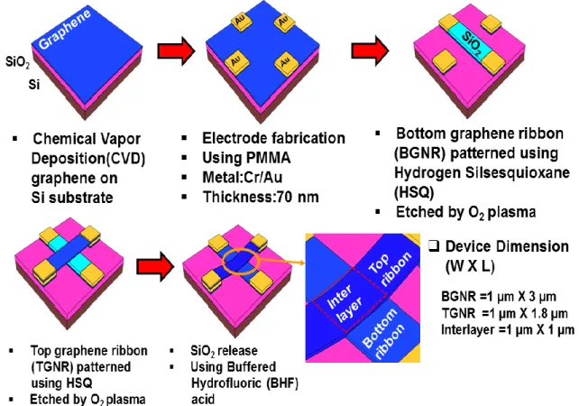
4.1 SAMPLE PREPARATION ... 54
4.2 4.2.1 Cleaning the CVD graphene ... 54
FABRICATION OF GRAPHENE-TO-GRAPHENE NEM CONTACT SWITCH ... 55
4.3 4.3.1 Fabrication of address pattern ... 55
4.3.2 Patterning of the graphene ribbon ... 57
4.3.3 Fabrication of contact electrodes ... 58
4.3.4 Deposition of SiO2 as a sacrificial layer ... 59
4.3.5 Transferring top graphene layer ... 59
4.3.6 Patterning the top graphene layer ... 60
4.3.7 Fabrication of the top contact electrodes ... 61
4.3.8 Releasing the sacrificial layer (SiO2) using the BHF ... 61
SUMMARY ... 63
4.4 GRAPHENE CROSSBAR DEVICE CHARACTERISATION ... 64
5 INTRODUCTION... 64
5.1 INTRODUCTION TO CROSSBAR DEVICE ... 65
5.2 FABRICATION OF GRAPHENE CROSSBAR DEVICE ... 65
5.3 RAMAN SPECTROSCOPY OF CROSSBAR DEVICE ... 66
5.4 ELECTRICAL CHARACTERISATION OF CROSSBAR DEVICE ... 67
5.5 5.5.1 Measurement configuration of the crossbar device ... 67
5.5.2 Results and discussion. ... 69
SUMMARY ... 76
5.6 GRAPHENE-TO-GRAPHENE NEM CONTACT SWITCH: 6 CHARACTERIZATION AND ANALYSIS ... 77
INTRODUCTION... 77
6.1 DEVICE STRUCTURE AND DIMENSION ... 78
6.2 RESULTS AND DISCUSSION ... 79
6.3 6.3.1 Pull-in characterization ... 79
6.3.3 Pull-in voltage variation in the different devices with similar structural dimension. ... 86
6.3.4 Fluctuation in the pull-in and pull-out voltages in different cycles of
switch. 89
6.3.5 Sub 1-V graphene NEM contact switch ... 89 6.3.6 Pull-out characterisation ... 91 CHAPTER SUMMARY ... 95 6.4
CONCLUSION AND FUTURE WORK ... 96 7
CONCLUSION ... 96 7.1
FUTURE WORKS ... 97 7.2
REFERENCES ... 99 8
LIST OF TABLES
TABLE 3.1.NEMSWITCH DIMENSIONS ... 45 TABLE 6.1.DEVICE PARAMETERS OF NINE MEASURED G_GNEM CONTACT SWITCHES. . 79 TABLE 6.2.STATISTICAL ANALYSIS OF THE PULL-IN VOLTAGES OF ALL DEVICES. ... 84 TABLE 6.3.SUMMARY OF ELECTRICAL CHARACTERIZATION OF ALL THE DEVICES. ... 85 TABLE 6.4.MISALIGNMENT INDUCED PULL-IN VOLTAGE VARIATION ... 88
LIST OF FIGURES
FIGURE 1.1 EVOLUTION OF MICROELECTRONICS DEVICES SINCE THE TIME OF FIRST INTEGRATED CIRCUITS IN 1958.ON THE LEFT Y-AXIS, THE NUMBER OF TRANSISTORS PER CHIP, AND THEIR CRITICAL DIMENSION (GATE LENGTH)(RIGHT-HAND SIDE) ARE
REPORTED. 20
FIGURE 1.2.THE TREND OF POWER CONSUMPTION WITH CMOS SCALING.REPRODUCED
FROM (WITHOUT PERMISSION)[2] 20
FIGURE 1.3.(A)SCHEMATIC OF THE SUBTHRESHOLD SLOPE OF CMOS DEVICE.(B)EFFECT OF SCALING IN THE COMS DEVICE. IOFF ' IS AN INCREASED DRAIN CURRENT AS A
RESULT OF THE GATE SCALING. 22
FIGURE 1.4. (A) THE INITIAL STRUCTURE OF THE NEM CONTACT SWITCH (DOUBLE CLAMPED BEAM STRUCTURE IS SHOWN). (B)NEM CONTACT SWITCH IS IN ON STATE.
24 FIGURE 1.5. AN OUTPUT CHARACTERISTIC OF THE NEM CONTACT SWITCHES (A) PULL-
IN/PULL-OUT CURVES IN THE REGARDING DISPLACEMENT. (B) PULL-IN/PULL-OUT
CURVES IN THE REGARDING MEASUREMENT. 25
FIGURE 1.6. COMPARISON OF OUTPUT CHARACTERISTICS. (A) SWITCHING CHARACTERISTICS OF NEM CONTACT SWITCH WITH CMOS SWITCH (THE BLUE CURVE IS FOR CONVENTIONAL CMOS, THE RED CURVE IS FOR NEM CONTACT SWITCHING).(B)ILLUSTRATING THE BOTH NEM CONTACT SWITCH CMOS SWITCH IN
THE SAME FRAME. 25
FIGURE 1.7UTILIZING GRAPHENE TO BUILD ALL-DIMENSIONAL CARBON MATERIALS. 26 FIGURE 2.1.1D PARALLEL PLATE MODEL OF NEM CONTACT SWITCH. 33 FIGURE 2.2. SCHEMATIC EXPLANATION OF THE EQUILIBRIUM MECHANICAL AND
ELECTROSTATIC FORCE. 35
FIGURE 2.3. SCHEMATIC EXPLANATION OF THE EQUILIBRIUM MECHANICAL AND
ELECTROSTATIC FORCE AT PULL-IN CONDITION. 36
FIGURE 2.4. 1D PARALLEL PLATE MODEL TO CALCULATE THE VOLTAGE OF PULL-OUT
EFFECT. 37
FIGURE 3.1.SCHEMATIC OF DOUBLE-CLAMPED GRAPHENE BEAM NEM SWITCH WITH TOP
METAL ACTUATION ELECTRODE. 46
FIGURE 3.2. THE GEOMETRY OF NEM SWITCH A. (A) INITIAL STRUCTURE OF DOUBLE-
CLAMPED GRAPHENE BEAM NEM SWITCH WITH A TOP METAL ELECTRODE. (B) PULLED-IN STATE OF THE GRAPHENE BEAM; COLOR BAR INDICATES THE RELATIVE DISPLACEMENT WITH RESPECT TO THE INITIAL CONDITION. 47 FIGURE 3.3.PULL-IN/PULL-OUT SWITCHING CHARACTERISTICS OF THE DOUBLE-CLAMPED
GRAPHENE BEAM NEM SWITCHES.(A)SWITCHING CHARACTERISTICS OF GRAPHENE BEAM NEM SWITCHES A,B, AND C.(B)SWITCHING CHARACTERISTICS OF GRAPHENE BEAM NEM SWITCH A, WITH DIFFERENT GRAPHENE THICKNESS OF T =3 NM,5 NM,
AND 9 NM. 47
FIGURE 3.4. VON MISES STRESS OF DOUBLE-CLAMPED GRAPHENE BEAM NEM SWITCHES. (A) VON MISES STRESS OF GRAPHENE NEM SWITCHES A,B, AND C.(B) VON MISES STRESS OF GRAPHENE BEAM NEM SWITCH A, WITH DIFFERENT GRAPHENE
THICKNESSES OF T =3 NM,5 NM, AND 9 NM. 48
FIGURE 3.5.CONTOUR PLOT (TOP VIEW OF GRAPHENE BEAM) OF VON MISES STRESS FOR THE NEM SWITCH A, WITH DIFFERENT GRAPHENE BEAM THICKNESSES OF T =3 NM,5
NM, AND 9 NM. 49
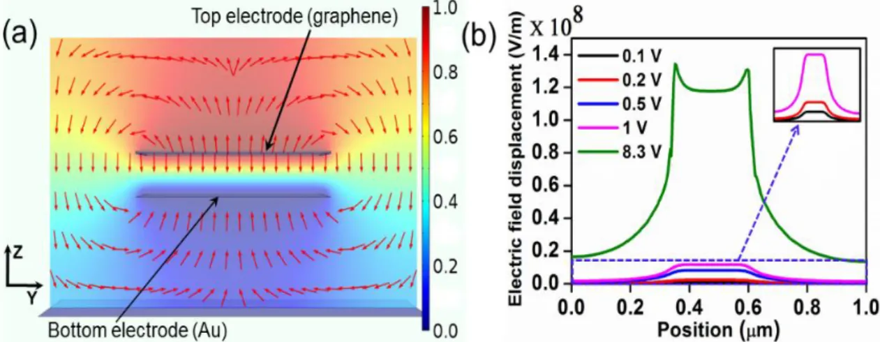
FIGURE 3.6. 2D ELECTRIC FIELD DISTRIBUTION ACROSS THE CENTER OF THE NEM
SWITCH.DIMENSIONS OF THE GRAPHENE BEAM (TOP ELECTRODE) ARE EQUIVALENT TO THOSE OF THE NEM SWITCH A. (A)THE ELECTRIC FIELD DISTRIBUTION ACROSS THE SWITCH AT THE CENTER OF THE BEAM.ARROWS INDICATE THE ELECTRIC FIELD DIRECTION.(B)THE ELECTRIC FIELD STRENGTH IN THE Z DIRECTION AT 5 NM ABOVE THE BOTTOM ELECTRODE AT DIFFERENT VOLTAGES APPLIED BETWEEN THE BOTTOM AND TOP ELECTRODES.THE INSET SHOWS ZOOMED-IN VERSION OF ELECTRIC FIELD DISTRIBUTION FOR LOWER ACTUATION VOLTAGES AS INDICATED BY THE DASHED
BOX; THE SCALE IS SAME AS (B). 50
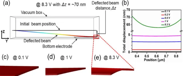
FIGURE 3.7.EFFECT OF THE BEAM EDGE ELECTRIC FIELD TERMINATION AT 8.3V.(A)THE DISPLACEMENT OF THE BEAM AT 8.3 V SHOWN AS A SIDE VIEW. (B) THE DISPLACEMENT OF THE BEAM FROM AN INITIAL POSITION AT DIFFERENT APPLIED VOLTAGES.BIRDS-EYE CROSS SECTIONAL VIEW OF THE GRAPHENE BEAM AT (C)0.1
V,(D)1V, AND (E)8.3V. 51
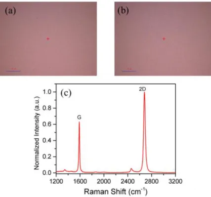
FIGURE 4.1(A) AND (B) OPTICAL MICROSCOPY IMAGES OF CVD GRAPHENE SAMPLE FROM
GRAPHENE PLATFORM. (C) A RAMAN SPECTRUM COLLECTED FROM ONE OF OUR
CVD SAMPLES. 54
FIGURE 4.2.CVD GRAPHENE ON SI/SIO2 SUBSTRATE. 57
FIGURE 4.3.PATTERNED GRAPHENE RIBBON. 57
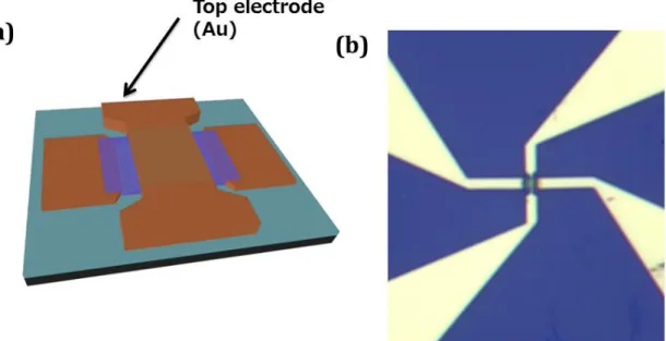
FIGURE 4.4. FABRICATION OF GOLD ELECTRODES.(A)SCHEMATIC ILLUSTRATION OF THE GOLD ELECTRODE FABRICATION. (B) OPTICAL MICROSCOPE OF THE DEVICE AFTER
THE GOLD ELECTRODE FABRICATION. 58
FIGURE 4.5.DEPOSITION OF SIO2LAYER. 59
FIGURE 4.6.TRANSFERRED THE TOP GRAPHENE LAYER. 60
FIGURE 4.7.PATTERN THE TOP GRAPHENE LAYER. 60
FIGURE 4.8. FABRICATION OF TOP ELECTRODES. (A) SCHEMATIC OF THE DEVICE STRUCTURE AFTER THE TOP ELECTRODE FABRICATION. (B) OPTICAL MICROSCOPE
IMAGE OF THE DEVICE. 61
FIGURE 4.9.SUSPENDED GRAPHENE RIBBON AFTER THE BHF RELEASE. 62 FIGURE 5.1. SCHEMATIC OF FABRICATION FLOW OF THE GRAPHENE-TO-GRAPHENE
CROSSBAR DEVICE. 66
FIGURE 5.2. (A) RAMAN SPECTROSCOPY OF THE GRAPHENE CROSSBAR DEVICE. (B) 2D PEAK SHIFT OF THE GRAPHENE CROSS BAR DEVICE (COMPARED WITH THE SINGLE
LAYER GRAPHENE SLG). 67
FIGURE 5.3. ELECTRICAL MEASUREMENT CONFIGURATION OF THE INTERLAYER
RESISTANCE MEASUREMENT SETUP. 68
FIGURE 5.4. EQUIVALENT CIRCUIT MODEL OF CROSS JUNCTION DEVICE. (A) IDEAL
CIRCUIT.(B)REAL CIRCUIT 68
FIGURE 5.5. BACK GATE CHARACTERISTICS OF THE GRAPHENE CROSSBAR DEVICE. (A) BOTTOM GRAPHENE RIBBON.(B)TOP GRAPHENE RIBBON. 69 FIGURE 5.6.BACK GATE CHARACTERISTICS OF THE GRAPHENE CROSSBAR DEVICE AFTER
VACUUM ANNEALING.(A)BOTTOM GRAPHENE RIBBON.(B)TOP GRAPHENE RIBBON. 70 FIGURE 5.7.BACK GATE CHARACTERISTICS OF THE GRAPHENE CROSSBAR DEVICE AFTER
HYDROGEN ANNEALING. (A) BOTTOM GRAPHENE RIBBON. (B) TOP GRAPHENE
RIBBON. 70
FIGURE 5.8. TEMPERATURE DEPENDENCE BACK GATE CHARACTERISTICS OF THE GRAPHENE CROSSBAR DEVICE AS FABRICATED.(A)BOTTOM GRAPHENE RIBBON.(B)
TOP GRAPHENE RIBBON. 71
FIGURE 5.9TEMPERATURE DEPENDENCE BACK GATE CHARACTERISTICS OF THE GRAPHENE CROSSBAR DEVICE AFTER THE IN-SITU ANNEALING PROCESS.(A)BOTTOM GRAPHENE
RIBBON.(B)TOP GRAPHENE RIBBON. 71
FIGURE 5.10. INTERLAYER RESISTANCE AS A FUNCTION OF THE BACKGATE VOLTAGE.(A) THE INTERLAYER RESISTANCE OF THE GRAPHENE CROSSBAR DEVICE FOR THE AS FABRICATED SAMPLE.(B)INTERLAYER RESISTANCE AFTER THE IN-SITU ANNEALING.
72 FIGURE 5.11.INTERLAYER RESISTANCE AS A FUNCTION OF THE TEMPERATURE. 72 FIGURE 5.12. SCHEMATIC DIAGRAM OF THE TEMPERATURE DEPENDENCE OF THE
INTERLAYER CONDUCTION MECHANISM. 73
FIGURE 5.13. SCHEMATIC DIAGRAM OF INTERLAYER CONDUCTION. (A) METAL- INSULATOR-METAL MODEL OF INTERLAYER TRANSPORT.(B)THE EFFECT OF IN-SITU
ANNEALING IN THE INTERLAYER TRANSPORT. 74
FIGURE 5.14. (A) INTERLAYER RESISTANCE IN THE AR+H2 GAS ENVIRONMENT. (B)INTERLAYER RESISTANCE AS A FUNCTION OF THE TEMPERATURE IN THE AR+H2
GAS ENVIRONMENT. 75
FIGURE 6.1. SCHEMATIC DIAGRAM OF THE GRAPHENE-TO-GRAPHENE TO NEM CONTACT SWITCH. THE INSET SHOWS THE FIXED GOLD ELECTRODE WITH GRAPHENE AS THE
CONTACT MATERIAL. 78
FIGURE 6.2.(A)AFM IMAGE OF THE DEVICE D1.(B)SEM IMAGE OF THE DEVICE D1. 78 FIGURE 6.3.TWO TERMINAL ELECTRICAL MEASUREMENT CONFIGURATION. 80 FIGURE 6.4. TYPICAL SWITCHING CHARACTERISTICS OF THE GRAPHENE-TO-GRAPHENE
NEM CONTACT SWITCH.(FIRST SWITCHING CYCLE OF DEVICE D1) 80 FIGURE 6.5.SWITCHING CHARACTERISTICS OF GRAPHENE-TO-GRAPHENE NEM CONTACT
DEVICE (DEVICE D1 TO D6 IS SHOWN) 81
FIGURE 6.6.SWITCHING CHARACTERISTICS OF GRAPHENE-TO-GRAPHENE NEM CONNECT
THE DEVICE (DEVICE D7 TO D9 IS SHOWN). 82
FIGURE 6.7.STATISTICAL AVERAGE OF THE PULL-IN VOLTAGE FOR DEVICE D1-D6. 83
FIGURE 6.8.STATISTICAL AVERAGE OF THE PULL-IN VOLTAGE FOR DEVICE D7-D9. 84 FIGURE 6.9. SUMMARY OF THE DEVICE D1- D9. (A) PULL-IN VOLTAGE AND THE
SWITCHING CYCLE OF THE DEVICES FROM D1 TO D9. (B)THE SWITCHING VOLTAGE
WINDOW OF THE DEVICES FROM D1 TO D9. 86
FIGURE 6.10. (A-F) SEM IMAGES OF THE DIFFERENT DEVICES WITH A MISALIGNMENT INDUCED SHIFT IN THE ACTUATION ELECTRODE.(D-F)SCHEMATIC REPRESENTATION OF THE ACTUATION ELECTRODE SHIFT IN DIFFERENT DEVICES. 87 FIGURE 6.11. THE GEOMETRY OF NEM SWITCH A. (A) INITIAL STRUCTURE OF DOUBLE-
CLAMPED GRAPHENE BEAM NEM SWITCH WITH A TOP METAL ELECTRODE. (B) PULLED-IN STATE OF THE GRAPHENE BEAM; COLOR BAR INDICATES THE RELATIVE DISPLACEMENT WITH RESPECT TO THE INITIAL CONDITION. 88 FIGURE 6.12. SWITCHING CHARACTERISTICS OF THE GRAPHENE NEM CONTACT SWITCH
WITH DIFFERENT MISALIGNMENT. 88
FIGURE 6.13. (A) SWITCHING CHARACTERISTICS OF THE DEVICE D9. THE PULL-OUT
VOLTAGE FLUCTUATION OF THE DEVICE D9. 89
FIGURE 6.14. (A) AFM IMAGE OF THE GRAPHENE RIBBON WITH SIO2 DEPOSITION. (B) AFM LINE PROFILE OF THE AFTER SIO2DEPOSITION. 90 FIGURE 6.15.SWITCHING CHARACTERISTICS OF THE SUB 1-V SWITCH.(A)SWITCH WITH
PULL-IN VOLTAGE OF 0.92V.(B)SWITCH WITH PULL-IN VOLTAGE OF 0.8V. 90 FIGURE 6.16.SURFACE ADHESION IN GRAPHENE- GOLD SURFACE.(A)GRAPHENE BEAM IS
PULLED ON TO THE SURFACE OF THE GOLD. (B) PULL-IN CHARACTERISTICS OF THE
NEM CONTACT SWITCH WITH AU AS CONTACT MATERIAL. (B) TYPICAL PULL OUT CHARACTERISTICS OF THE PULL-OUT IN THE NEM CONTACT SWITCH WITH AU AS THE
CONTACT MATERIAL. 91
FIGURE 6.17.SURFACE ADHESION IN GRAPHENE-CR2O3SURFACE.(A)GRAPHENE BEAM IS PULLED ON TO THE SURFACE OF THE CR2O3.(B)PULL-IN CHARACTERISTICS OF THE
NEM CONTACT SWITCH WITH CR2O3 AS CONTACT MATERIAL.(B)TYPICAL PULL OUT CHARACTERISTICS OF THE PULL-OUT IN THE NEM CONTACT SWITCH WITH CR2O3 AS
THE CONTACT MATERIAL. 92
FIGURE 6.18.SURFACE ADHESION IN THE GRAPHENE-GRAPHENESURFACE.(A)GRAPHENE BEAM IS PULLED ONTO THE SURFACE OF THE GRAPHENE. (B) PULL-IN CHARACTERISTICS OF THE NEM CONTACT SWITCH WITH GRAPHENE AS CONTACT
MATERIAL.(B)TYPICAL PULL OUT CHARACTERISTICS OF THE PULL-OUT IN THE NEM
CONTACT SWITCH WITH GRAPHENE AS THE CONTACT MATERIAL. 93
Introduction 1
M
OORE`S LAW ANDCMOS L
IMITATIONS1.1
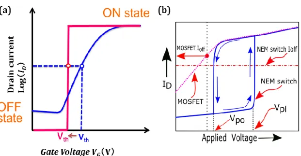
Complementary Metal Oxide Semiconductor (CMOS) technology has been miniaturized to nano scale according to Moore’s law [1]. The Moore’s law expressed that, the number of transistors in a silicon integrated circuit (IC) increased to twice the quantity for every 18 months and also the gate length of the MOS transistor reduced to half [2]. Figure 1.1 illustrates the number of transistor per processor chip vs. year. It is evident from the Figure 1.1; the scaling is in good agreement with Moore’s law. The CMOS scaling gradually improves the performance of the Very Large Scale Integration (VLSI) circuits and systems [3]. However, the CMOS scaling introduces the heat dissipation problem. The amount of heat released from the IC has been increased with the CMOS scaling. The heat dissipation is critical issue. The heat dissipation problem is difficult to solve with scaling. It is Because of the subthreshold swing, how sharply the drain current drops with the applied gate voltage, of the Metal- oxide-semiconductor field effect transistor (MOSFET). The slope of the subthreshold swing is limited to 60 mV/dec at 300K [4]. It is exceptionally hard proportional down the drain voltage VD less than sub 1 V while expanding the speed of the MOSFET and keeping the power dissipation in very low range. Scaling is difficult without reducing the applied voltage because the charge control is difficult. The reduction of the channel length gives rise to unwanted short-channel effects (SCE). When the length of channel is shortened, drain bias affects the channel potential than the long channel device. Due to this channel bias, the potential barrier is reduced, this phenomenon is called drain- induced barrier lowering (DIBL). To effectively control short channel device by the
thickness of the gate oxide is only 1.2 nm. Moreover, band-to-band tunneling occurs because of drastically reducing gate oxide to low thickness, which upsurges the gate leakage. For MOSFET with 40 nm gate length, the leakage power dissipation has tantamount to dynamic power dissipation, Figure 1.2, displays the off-state leakage power and the dynamic power with scaling [5].
Figure 1.1 Evolution of microelectronics devices since the time of first integrated circuits in 1958. On the left Y-axis, the number of transistors per chip, and their critical dimension (gate length) (right-hand side) are reported.
Figure 1.2.The trend of Power consumption with CMOS scaling. Reproduced from (without permission) [2]
1.1.1 T
HE ENERGY EFFICIENCY LIMIT OF THECMOS
The MOSFET is the fundamental functional unit of the VLSI Integrated Circuits (IC’s). The MOSFET is an active device. The active device has three terminals. There is source terminal, drain terminal and the gate. The channel is formed between the source and drain terminal. The current flow in the channel is controlled by the gate. The potential barrier is shaped between the source and drain interface in the off state. The current flow in the channel is caused by the diffusion of charge carriers. The height of the potential barrier determines a number of charge carriers that flow through the channel. The drain collects the mobile charge carriers. By controlling the gate voltage, height of the potential barrier is modulated, which controls the current moving over the channel [6].
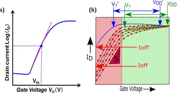
The current that flows through the channel of the MOSFET is referred as the drain current (I
D). The transfer characteristic of a MOSFET is shown in Figure 1.3. The applied gate voltage (V
G) increased beyond the threshold voltage (V
TH), the height of the potential barrier is reduced. Once the potential barrier is reduced, then charge carriers freely maneuver from the source into the channel area. In the on case, mobile charge carriers make the conductive path along the channel region. The drift in the state channel limits the current flow through the channel. The following equation gives the on-current (ION) of a long-channel MOSFET:
( )2
ON eff ox DD th
I C W V V
L
(1.1)
eff - Effective carrier mobility, Cox - Capacitance (gate oxide) per unit area, W - Width of the channel and L - Length of the channel.
The Figure 1.3a shows the drain current (ID) over gate voltage (VG). It can be evident from the Figure 1.3a, that the transition of the drain current (ID) from off-state to on-state is not an abrupt one. Boltzmann statistics represents the dissemination of energy of charge carriers in source area. So, the subthreshold (VG < VTH) region of operation, diffusion of charge carriers (and hence ID) increases exponentially with increasing VG. The increasing VG reduces the potential barrier.
The off-state leakage current (IOFF) is given by:
I
OFF 10
Vth/SS (1.2)Moreover, the subthreshold swing (SS) is described as the inverse slope of the ID-VG curve,
ln(10) 1 dep
ox
kT C
SS q C
(1.3) kT
q - thermal voltage ; 1 dep
ox
C
C - factor from the depletion capacitance. The oxide capacitance is higher than that of the depletion capacitance of the semiconductor.
So the sub threshold slope reduces to, which is 60mV/dec at room temperature. The common MOSFET switching characteristic constrained to be no more acute than the 60mV/dec as because kT
q
is the non-scaling physical quantity. In practical MOSFET switches, the subthreshold swing is typically more than 100mV/dec. The non-scalability of physical quantity sets the fundamental limit on the subthreshold swing. The subthreshold swing tells how suddenly a MOSFET can switch make a transition from the ON state to OFF state. The Figure 1.3a shows the transfer characteristics of the MOSFET. The Figure 1.3b shows the, increase in the leakage current (Ioff’) due to the CMOS scaling [3].
Figure 1.3. (a) Schematic of the subthreshold slope of CMOS device. (b) Effect of scaling in the COMS device. Ioff ' is an increased drain current as a result of the gate scaling.
The total amount of the energy dissipated in the digital CMOS circuits is divided into two main parts. First, the dynamic energy (𝐸𝐷𝑌𝑁𝐴𝑀𝐼𝐶), the dynamic energy is comes from either charging or discharging capacitors. Second, leakage energy (𝐸𝐿𝐸𝐴𝐾𝐴𝐺𝐸) is generated by off-state leakage current of the MOSFET. The total energy dissipated in the CMOS circuits are given by,
TOTAL DYNAMIC LEKAGE
E E E (1.4)
2
DYNAMIC D DD
E L fCV (1.5)
LEAKAGE D OFF DD
E L fI V t (1.6)
𝛼 - the activity factor, 𝐿𝐷 - logic depth, 𝑓 - fan-out and 𝐶 - capacitance, and t - time delay.
Reducing the VDD can reduce the dynamic energy, which means MOSFET ON current (𝐼𝑂𝑁) is also reduced. The reducing the VDD also increases the time delay (𝑡𝐷𝐸𝐿𝐴𝑌). To retain the same ON current, the threshold voltage (𝑉𝑇𝐻) should be minimized. Nonetheless, according to Subthreshold Swing, when the threshold voltage (𝑉TH) is reduced linearly the off-state leakage (𝐼𝑂𝐹𝐹) will increase exponentially.
The panacea to power crisis issue of CMOS devices is a need of new sort of device that has a perfect exchange of conventional CMOS. The new device should possess characteristics of ideal switching. An ideal switch should have abrupt on/off ratio, stable on current, and no leakage current. The Mechanical switching is the proposed solution for the CMOS power crisis. In the mechanical switching, the active element and the fixed electrode are separated by the air gap. This physical separation between suspended beam and the fixed electrode ensures the low off current. And this will lead to the very low leakage. As the leakage is extremely small, the ELEAKAGE
becomesnegligible. So the total energy only depends on the dynamic energy [7].
N
ANO-
ELECTRO-
MECHANICALS
WITCHING: S
TATE OF THE1.2
A
RT1.2.1 O
PERATINGP
RINCIPLE OF MECHANICAL SWITCHINGThe device structure of double clamped NEM contact switch is shown in Figure 1.4. Several device structures are available to realize the NEM contact switch. The two primary device type is cantilever type, and double clamped type (resonator). In the
double clamped beam NEM contact switch, there are two elements, one is a fixed element, and the other one is a movable/active element (suspended beam) as shown in Figure 1.4a. The fixed element and suspended element both are separated by an air gap.
The voltage is enforced between fixed element suspended beam; the suspended beam begins to deflect towards the fixed element is attributable to the electrostatic force between the fixed electrode and the suspended beam. To understand the pull-in phenomenon consider only the two most important forces in the device; electrostatic force due to the applied voltage and restoring force of the suspended beam. The origin of the restoring force is effective spring constant of the suspended beam. When the given voltage is maximized beyond a certain value, the restoring force no longer can effectively balance the electrostatic force; the suspended beam suddenly deformed to the fixed electrode [8]. This abrupt deflection of the suspended beam gives the sharp rise in the current. The current is referred as the switching current. The switching slope is very steep [9]. The Figure 1.4a shows the OFF state of the NEM contact switch and the ON state of the NEM contact switch is shown Figure 1.4b.
Figure 1.4. (a) The initial structure of the NEM contact switch (double clamped beam structure is shown). (b) NEM contact switch is in ON state.
The switching characteristics of NEM contact switch are shown in Figure 1.5. The switching characteristics regarding the beam displacement are shown in the Figure 1.5a.
When the voltage is increased between the fixed electrode and the suspended beam, suspended beam moves towards the fixed electrode gradually up to certain limit, snap-in point. After the snap-in point, the suspended beam abruptly deflects to the fixed electrode. When the voltage is decreased, the restoring force overwhelms the electrostatic force; the pulls the suspended beam to its original position. The immediate collapse of the suspended beam on to the fixed electrode gives the very sharp rise in the current between the fixed electrode and the suspended beam. The switching
characteristics regarding the switching current are shown in the Figure 1.5b. The hysteresis is formed between the switch ON state and the switch OFF state due to the contact force [10].
Figure 1.5. An output characteristic of the NEM contact switches (a) Pull-in/Pull-out curves in the regarding displacement. (b) Pull-in/Pull-out curves in the regarding measurement.
Figure 1.6. Comparison of output characteristics. (a) Switching characteristics of NEM contact switch with CMOS switch (the blue curve is for conventional CMOS, the red curve is for NEM contact switching). (b) Illustrating the both NEM contact switch CMOS switch in the same frame.
The Figure 1.6a illustrates the switching characteristics of the CMOS MOSFET and the mechanical switch. Figure 1.6b shows the combination of the switching characteristics of CMOS and NEM contact switch [10].
G
RAPHENE1.3
Graphene is an atomically-thick two-dimensional (2D) material, which consists of the hexagonal lattice which is made up of carbon atoms [11]. Graphene is a single layer form of the bulk material graphite, which can be easily found from the pencil lead.
Monolayer graphene was exfoliated from the graphite, by using the scotch tape.
The first single layer graphene properties are demonstrated by Dr. Andre Geim and Dr.
Konstantin Novoselov, for which they were awarded the Nobel Prize in Physics (2010).
The different forms for the carbon atoms are shown in Figure 1.7. The graphene additionally can also be grown by the Chemical Vapor Deposition (CVD) technique.
The quality of the CVD grown graphene is not similar to that of the exfoliated graphene layer. The single layer graphene is a zero band gap material [12], [13].
Figure 1.7 Utilizing graphene to build all-dimensional carbon materials.
1.3.1 E
LECTRICAL PROPERTIES OF GRAPHENEGraphene has exclusive band structure. It is a zero band gap material [12]. The conduction band and valence band of graphene are connected at one point, known as the Dirac point, or the charge neutral point. Moreover, the linear dispersion relationships are observed from both the conduction band and valence band when the energy level is not far away from the charge neutral point. The effective electron mass of graphene is zero owing to the linear relationship of momentum k and energy E [11]. Due to this massless behavior, intrinsic suspended graphene possesses extremely high electron mobility, approaching to 200,000 cm2/Vs measured at the low temperature [14]. The electrical property of the graphene is layer dependent. The band gap of the bilayer graphene is tunable by the applying the electric field. Even the electronic properties of
the bilayer graphene are highly rotational dependent. The Bernal stacked bilayers exhibit the metallic behavior where as the twisted bilayer exhibits the semiconducting behavior [13].
1.3.2 M
ECHANICAL PROPERTIES OF GRAPHENEGraphene, a single atomic layer of material. The in-plane stiffness of graphene, 340 N/m, was characterized from freely suspended circular shaped membranes by using the nanoindentation method. Graphene possesses an impressively high Young’s modulus of 1 TPa [15]. The breaking tenacity was also reported from the same experiment, indicating to a bulk value of 130 GPa. Besides, breaking strain of 25% was investigated, and the graphene membranes were easy to be broken under the nonlinear elastic regime. In the case of NEMS study, the mechanical properties of the movable elements largely determine the performance and reliability of the device. These mechanical properties of graphene mentioned above are better than any of the thin-film materials under the use of NEM technology. Also, graphene has another merit which is resistance to the natural oxidation, revealing that graphene-based NEM device has better reliability compared with the device made from metals.
R
EVIEW OF THE RECENT LITERATURE1.4
In this section, some of the important literature are discussed. The NEM contact switches are a primarily a mechanical switch; the electrostatic forces between the fixed electrode and the suspended beam can activate the suspended element. The electrostatic force causes to deflect the suspended element mechanically, further forming a physical contact with the fixed electrode.
As the air gap physically separates the suspended beam and the fixed electrode, NEM contact switch can give low leakage current; NEM contact switch has many enormous advantages such as reduced power consumption and high ON/OFF ratio.
Also, the NEM contact switch can operate at high speeds with sub 1-V operation. NEM switches also have potential capability of working in the harsh environment like high radiation, external electric field, and temperature. The NEM switches have been widely explored for the several applications like a relay, a logic device [16], [17], transistor and sensor, which is consistent with these switches based on the conventional
semiconductor technology [18], [19]. Furthermore, the low reliability of the device performance mainly limited by the contact adhesive forces [8].
In this section, different types of NEM contact switches actuated by electrostatic force are reviewed and discussed.
Nanowire-based NEM switches: The nanowires are one of the prime material of choice for the NEM contact switches. The high-performance three-terminal NEM switching FET was successfully demonstrated, using the double clamped Ge/Si core shell nanowire, experimentally by the J.H. Kim et al. [20]. Clear pull-in/pull-out operations were observed with a subthreshold slope as low as 6mV/dec. The Ge/Si core shell nano wire NEM FET works in the very high- frequency range. Another important, silicon carbide nanowire based NEM contact switches are demonstrated by X.L. Feng et al. [21]. The NEM contact switches are fabricated with a highly small w air gap (~10 nm). Very low activation voltage is demonstrated with on/off ratio > 103.
Carbon Nanotube based NEM switches: Prof. Iijima discovered a single-wall CNT in 1991. In 2004, a two terminal CNT NEM switch was demonstrated by S. W. Lee et al. [22]. Multiwall CNT was used as the suspended material. The device is fabricated as the cantilever type. And the CNT was deflected to contact with drain electrode by applying gate voltage. Switching hysteresis was observed experimentally from this device. No precise switching characteristics were observed as the device shows inferior performance. The pull-in was observed at 5 V.
Graphene-based NEM switches: Graphene is regarded as the material to improve the performance of NEM switches due to its better electrical and mechanical properties. The graphene based NEM contact switch was demonstrated by K.M. Milaninia et al. in 2009 [23]. They utilized chemical vapor deposition (CVD) grown graphene. The CVD graphene was used to define both the moveable beam and bottom contact electrode. There is no precise switching was observed. Two years later, a graphene NEM switch with very low pull-in voltage (1.85 V) was demonstrated by S. M. Kim and his colleagues [24]. And their device fabrication showed the compatibility with the conventional CMOS technology. Based on the quantitative study of exfoliated graphene-based NEM switches by Zhang’s group, they found that monolayer graphene was not ideal for the NEM application since it was too easy to tear.
Multilayer graphene-based NEM switch worked with a point contact with the probe of Scanning Tunneling Microscope (STM), which reached high reliability among the graphene NEM switching devices (~500 cycles). Instead of double clamped structure, cantilever-type graphene NEM switches were also measured using both two-terminal and three-terminal measurement by P. Li and his colleagues [25]. However, the reliability was still a severe issue of device performance. A bilayer graphene-based NEM switch with local bottom electrode was achieved with very low pull-in voltage, 1.8 V was demonstrated by J.Sun et al. [26]. The device works only a very few cycle. And the graphene beam is stick to the fixed electrode. The stiction is attributed to the Au-C chemical bonding. To overcome the stiction issues in the graphene based NEM contact switches, the structurally engineering the contact surface was studied by W.Wang et al. [27]. The period trench pattern was introduced in the contact surface to overcome the surface adhesion. The stiction is one of the prominent failure modes in the graphene based NEM contact switches. As the NEM contact switches only work for the very few switching cycles, the failure mode cannot be the ablation. The ablation, in which the suspended beam was damaged by repeated contact cycles [22]–[26].
T
HEP
URPOSE OF THIS STUDY1.5
As based on the current research, NEM contact switch becomes one of the promising candidates for overcoming the limitations of conventional CMOS technology. The NEM contact switches can offer low leakage current, abrupt switching (SS < 5mV/dec) as well as high ON/OFF ratio. Conventional material (Si) based as well as the graphene based NEM contact switches facing lot problems. One among them is stiction induced failure in the NEM contact switches. Though graphene possesses the excellent electrical and mechanical properties, the conventional contact material (Au, Cr, Cr2O3) leads to stiction related failures in the NEM contact switches.
The adhesion force between the graphene and the conventional contact material leads to high energy barrier, which causes the irreversible stiction in the graphene based NEM contact switches. To avoid the irreversible stiction in the graphene based NEM contact switches, graphene layer as the contact material is proposed as a solution to prevent the irreversible stiction. It is also essential to understand the interaction between the
graphene layer, a graphene-to-graphene crossbar device is intended as a method to study the interlayer conduction between the graphene layers.
T
HESISS
TRUCTURE1.6
This dissertation composed into six chapters. The content of these sections is as per the following:
Chapter1: Introduction. This chapter discusses the origin of the crisis and fundamental limit of the CMOS MOSFET switching. The effect of the CMOS scaling. A different switching device with ideal switching characteristics, the NEM contact switches, is suggested as a solution for CMOS power crisis.
Further, it also introduces failure issues with the conventional contact NEM switches. The graphene-to-graphene NEM contact switch is proposed as a solution for the NEM contact switches.
Chapter2: Essential theory of the NEM contact Switches. In this chapter, the theory behind the mechanical switching is explained.
Chapter3: Theory and Finite Element Method (FEM) simulation of graphene based NEM contact switches. In this chapter, Finite Element Method (FEM) simulation is introduced. Further, finite element method (FEM) simulation of the graphene based NEM contact Switches is discussed in detail.
Chapter4: Fabrication of graphene-to-graphene NEM contact switches. In this chapter, provides essential detail about the CVD graphene. Then the fabrication process of graphene-to-graphene NEM contact switch is explained in step by step manner. The fabrication techniques such as Graphene transfer (wet chemical based transfer), BHF etching, and super critical point dryer also discussed in detail.
Chapetr5: Fabrication and characterisation of graphene cross bar device. In this chapter, the in-situ annealing effect on the interlayer conduction in graphene-to-graphane crossbar device is discussed. Also, the fabrication process of the graphene-to-graphene crossbar device, Raman spectroscopy of the interlayer (twisted bilayer) graphene, incoherent conduction in the misoriented graphene bilayer, in-situ annealing effect on the interlayer conduction, as well as the effect gas (Ar+H2) on the interlayer conduction in graphene-to-graphene crossbar device is discussed in detail.
Chapter6: Measurements and Characterization of Graphene-to-graphene NEM contact Switches. In this chapter, we presented the results of the graphene-to-graphene NEM contact devices with different dimensions.
Graphene-to-graphene NEM contact switch introduced experimentally for the first time. We extracted the switching slope for several devices which showed very steep switching of <10 mV/sec.Moreover, the graphene-to-graphene NEM contact switches show the stiction free switching characteristics.
Chapetr7: Summary and Future work: This chapter concludes the thesis, and also provide an outlook on future work regarding graphene based NEM contact switches.
Essential theory of NEM contact 2
switches.
I
NTRODUCTION2.1
In this chapter, the basic physics and related equations behind the switching mechanisms of NEM contact switches are introduced. Pull-in and pull-out conditions of the movable element, as the fundamental operations of NEM contact switches, are explained at first. The equations presented in this chapter are useful for designing NEM contact switches.
E
LECTROMECHANICALA
NALYSIS2.2
2.2.1 P
ULL-
IN ANALYSISFigure 2.1. 1D parallel plate model of NEM contact Switch.
Figure 2.1 shows a typical one-dimensional (1D) limped model approximation of parallel-plates for the mechanical contact switches. One plate is fixed and controlled by a voltage source, which is normally considered as the fixed actuation electrode. The other plate is a movable element/beam and is connected to a mechanical spring with spring constant K and also connected to ground electrically. The voltage is enforced between fixed actuation electrode and movable beam; electrostatic force is generated by because of the potential difference between the fixed and the movable beam. The electrostatic force causes the movable beam to be attracted to and approach the actuation electrode [32], [33].
The electrostatic force generated between the two plates is expressed as follows:
Felectrostatic = (2.1) - Vacuum permittivity
L - Length of beam W - Width of the beam
V - Applied voltage of the actuation electrode
- The initial air gap between the movable element and fixed electrode.
The mechanical motion of a movable element is modeled as a linear spring following the Hooke’s law, which acts as restoring force. The spring constant is
obtained by the geometry of the movable elements. The equation indicating a linear response of restoring mechanical motion of the movable element is shown below.
Frestoring = Kd (2.2) K - spring constant of the movable element;
d - displacement distance moved from anchored electrode from its original position.
For the study of NEM contact switches, double-clamped beam and single-clamped cantilever structure are often investigated. Spring constants of double-clamped beam and cantilever are expressed as [34], [35]:
Kdouble-clamped beam = (2.3) Kcantilever=
(2.4) Where E is Young's modulus of material used for the movable element, L and W are the length and width of its structure, respectively, and t is the thickness of beam or cantilever. The electromechanical system is mainly governed by the mechanical restoring force and electrostatic force. As the voltage is applied between the two electrodes, the movable element initially approaches the fixed electrode, since those two forces mentioned above are under equilibrium state. However, at a certain position (usually two-thirds of the original gap distance), the electrostatic force overwhelms the mechanical restoring force, resulting in a sudden collapse of the movable element on the electrode and a sharp increase of current. The phenomenon mentioned above is called pull-in effect, and we can calculate the pull-in voltage from the estimated electrostatic and restoring force at the position of two-thirds of original gap. The pull-in equation is shown below:
Vpull-in = √ (2.5) If we considered the spring constant of a double-clamped beam and cantilever into the estimation of pull-in voltage, the equations of pull-in voltage could be rewritten as:
Double-clamped beam: Vpull-in = √
(2.6) Cantilever: Vpull-in = √
(2.7)
2.2.2 T
HE EQUILIBRIUM POSITION OF THE ELECTROSTATIC ACTUATOR WITH APPLIED BIAS.
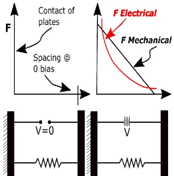
As discussed earlier, the electrostatic actuators have one deformable/ movable beam and a fixed electrode. It is essential to understand and determine the amount of static displacement under the applied bias voltage. To analyze the displacement position of the suspended/deformable beam, consider that the equilibrium position can be visualized as shown in Figure 2.2. The X-axis represents the space between the fixed electrode and the movable beam, and the Y-axis represents the force (electrical/mechanical). The movable beam is initially placed at the position X0. There are two curves, one represents the mechanical restoring force, and the other one represents the electrostatic force. The mechanical restoring force changes linearly with the position for any applied voltage. (The black line is shown in Figure 2.2) The electrostatic force varies nonlinearly with the position for any applied bias voltage (The red curve showed in Figure 2.2) [36]–[38].
Figure 2.2. Schematic explanation of the equilibrium mechanical and electrostatic force.
There are multiple intersecting points for the two curves, and the intersecting points are identical. The equilibrium position of the movable beam for different applied voltages is demonstrated graphically in Figure 2.3. As the voltage increases, the
corresponding electrostatic curves shift upwards. At a certain bias voltage, the mechanical restoring force and the electrostatic force intersect at one point tangentially.
At that point, the mechanical and electrostatic force equal each other. This condition is referred as the snap-in/ pull-in condition. Moreover, the effective force constant of the spring becomes zero. The voltage at this condition is referred as pull-in voltage [39], [40].
After this voltage, any infinitesimal change in the applied voltage leads to a sudden deformation of the movable beam on to the substrate due to the mechanical force being unable to overcome the electrostatic force.
Figure 2.3. Schematic explanation of the equilibrium mechanical and electrostatic force at pull-in condition.
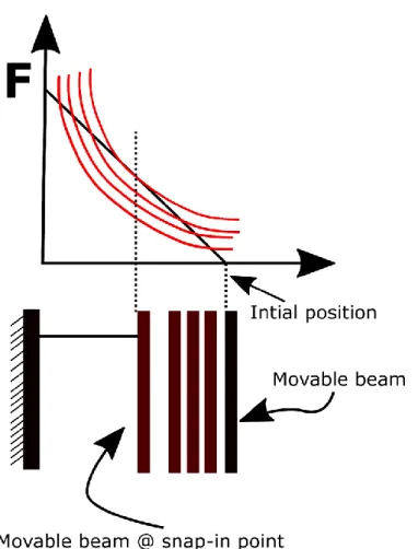
2.2.3 P
ULL-
OUT ANALYSISFor the pull-out operation, the assumed initial position of both plates is in contact, as shown in Figure 2.3. By applying a voltage, an electrostatic force is generated.The mechanical restoring force at this point obtains the highest value since the movable elemental is at maximum displacement from its original position. With the decrease of the voltage applied between the movable element and actuation electrode, the
electrostatic force is reduced. Once the mechanical-restoring force overcomes the electrostatic attraction force, the movable element will be detached from the actuation electrode. This process is called pull-out [41], [42].
Figure 2.4. 1D parallel plate model to calculate the voltage of pull-out effect.
Owing to the existence of dielectric oxide layer at the contact interface, the polarized dielectric layer governs the electrostatic force. Assuming the dielectric layer having a thickness tox, the pull-out voltage can be described by the equation below.
Vpull-out = √
(2.8) where is the relative permittivity of the dielectric oxide. This can also be applied with the spring constants of double-clamped beam and cantilever. The modified equations are listed below.
Double-clamped beam: Vpull-in = √
(2.9)
Cantilever: Vpull-in = √
(2.10) The analytical equations describing the pull-in and pull-out voltage rely on ideal conditions such as material properties and precise geometry used. In other words, these analytical models can be used for estimating or examining the proposed structures.
There are always some gaps between estimated values and experimental results, since several physical factors, such as short-range forces, dielectric charging effect, are not included in these models.
Finite Element Method (FEM) 3
simulation of graphene based
Nanoelectromechanical Switches
I
NTRODUCTION3.1
There are two main purposes of this chapter; firstly, the chapter is devoted to explaining the essential theory of Finite Element Method (FEM) simulation. It is worth to mention, most of the simulations in this thesis, and especially the Pull-in problem, are carried out by the commercial software IntelliSuite. So, the theory section mainly explains the essential theory behind the operation of the FEM software (IntelliSuite).
The second part of the chapter is devoted to the 3D finite element simulation of the graphene based NEM contact switches.
![Figure 1.2.The trend of Power consumption with CMOS scaling. Reproduced from (without permission) [2]](https://thumb-ap.123doks.com/thumbv2/123deta/6126475.1078984/23.892.86.702.700.1075/figure-trend-power-consumption-cmos-scaling-reproduced-permission.webp)