Japan Advanced Institute of Science and Technology
JAIST Repository
https://dspace.jaist.ac.jp/
Title
Fabrication of C_<60> field-effect transistors
with polyimide and Ba_<0.4>Sr_<0.6>Ti_,<0.96>O_3
gate insulators
Author(s)
Kubozono, Y; Nagano, T; Haruyama, Y; Kuwahara, E;
Takayanagi, T; Ochi, K; Fujiwara, A
Citation
Applied Physics Letters, 87(14):
143506-1-143506-3
Issue Date
2005-10
Type
Journal Article
Text version
publisher
URL
http://hdl.handle.net/10119/3374
Rights
Copyright 2005 American Institute of Physics.
This article may be downloaded for personal use
only. Any other use requires prior permission of
the author and the American Institute of Physics.
The following article appeared in Yoshihiro
Kubozono, Takayuki Nagano, Yusuke Haruyama, Eiji
Kuwahara, Toshio Takayanagi, Kenji Ochi and
Akihiko Fujiwara, Applied Physics Letters 87(14),
143506 (2005) and may be found at
http://link.aip.org/link/?apl/87/143506.
Fabrication of C
60field-effect transistors with polyimide
and Ba
0.4Sr
0.6Ti
0.96O
3gate insulators
Yoshihiro Kubozono,a兲 Takayuki Nagano, Yusuke Haruyama, Eiji Kuwahara, Toshio Takayanagi, and Kenji Ochi
Department of Chemistry, Okayama University, Okayama 700-8530, Japan and CREST, Japan Science and Technology Agency, Kawaguchi, 322-0012, Japan
Akihiko Fujiwara
Japan Advanced Institute of Science and Technology, Ishikawa 923-1292, and CREST, Japan Science and Technology Agency, Kawaguchi, 322-0012, Japan
共Received 21 June 2005; accepted 8 August 2005; published online 29 September 2005兲
A flexible C60 field-effect transistor 共FET兲 device has been fabricated with a polyimide gate insulator on the poly共ethylene terephthalate兲 substrate, and n-channel normally off FET properties are observed in this FET device. The field-effect mobility,, is estimated to be⬃10−2cm2V−1s−1 at 300 K. Furthermore, the C60 FET has been fabricated with a high-dielectric Ba0.4Sr0.6Ti0.96O3 共BST兲 gate insulator, showing n-channel properties; the value is estimated to be ⬃10−4cm2V−1s−1 at 300 K. The FET device operates at very low gate voltage, V
G, and low
drain-source voltage, VDS. Thus these C60FET devices possess flexibility and low-voltage operation characteristic of polyimide and BST gate insulators, respectively. © 2005 American Institute of
Physics. 关DOI:10.1063/1.2081134兴
Field-effect transistors 共FETs兲 with thin films of fullerenes have been extensively studied during the past decades,1–12and the potential applications of fullerene FETs in next-generation electronic devices have been discussed based on their high values of field-effect mobility, . The first fullerene FET device was fabricated with thin films of C60and a SiO2gate insulator by Haddon et al.1This device showed n-channel properties and a high value of 0.08– 0.30 cm2V−1s−1. Subsequently, Haddon developed the C70FET device with the SiO2gate insulator which exhibited the n-channel performance with the value of 2 ⫻10−3cm2V−1s−1.2
The value of the C60 FET device reached 0.56 cm2V−1s−1共Ref. 3兲, which was comparable to the highest value realized so far in the n-channel FETs with thin films of organic molecules共OFETs兲 共Ref. 13兲.
The characteristics such as shock-resistance, structural flexibility, large-area coverage, and portability are the most important advantages expected for the OFETs. Therefore, it is necessary for the SiO2/ Si substrate to be replaced by poly-mer gate insulators in a realization of the complete flexible OFET devices. In 2004, Someya et al. successfully fabri-cated the flexible and high-performance p-channel pentacene FET device with polyimide gate insulator.14The flexible and high-performance n-channel OFET device is required for a realization of the flexible complementary metal-oxide-semiconductor logic gate circuit, which has many advantages such as low-power consumption, good-noise margin, and ease of design.15
The C60FET device with a high-dielectric gate insulator such as Ba0.4Sr0.6Ti0.96O3共BST兲 attracts special attention for high-carrier injection into the channel region of C60 thin films, because the doping of electrons and holes into C60 is expected to yield new materials with novel physical proper-ties, from the analogy with metal-intercalated C60exhibiting superconductivity and metallic behavior. Such novel physical
properties are produced by the electron filling to the lowest unoccupied molecular orbital 共LUMO兲 of the C60 molecule.16 Currently, the number of electrons that can be injected into the C60 molecules by field-effect doping is at most 0.1 per C60molecule even at the maximum gate voltage
VGmax, because of the low-dielectric constant x 共⬃3.9兲 of
SiO2 used as an insulating layer. Therefore, new techniques for high-carrier injection, i.e., injection of more than one electron or hole per C60molecule, are required to control the electronic structure of C60.
The maximum density of carriers, Nmax共cm−2兲, which can be induced on the dielectric insulating layer, is empiri-cally given by Nmax⬃1.1⫻1013x
1/2
since VG
max 共MV兲 ⬃dEmax⬃20d/x1/2; d共cm兲 is the thickness of the insulating
layer. The high-carrier injection into C60thin film in the FET device should be realized by using the highxgate insulator.
Furthermore, the high-carrier injection into the active layer should achieve the low gate voltage 共VG兲 and low
drain-source voltage共VDS兲 operation in the FET device. The
low-voltage operation is very important in a realizing the practi-cal FET device, because the VG and VDS required for
operation of the OFET device are currently as high as 10– 100 V. In the present study, the C60 thin-film FET de-vices with polyimide and BST gate insulators have been fab-ricated on the poly共ethylene terephthalate兲 共PET兲 and the Si substrates, respectively. The fabrication of these FET devices should open a way to the structural flexibility and the low VG
and VDSoperation in the OFET device.
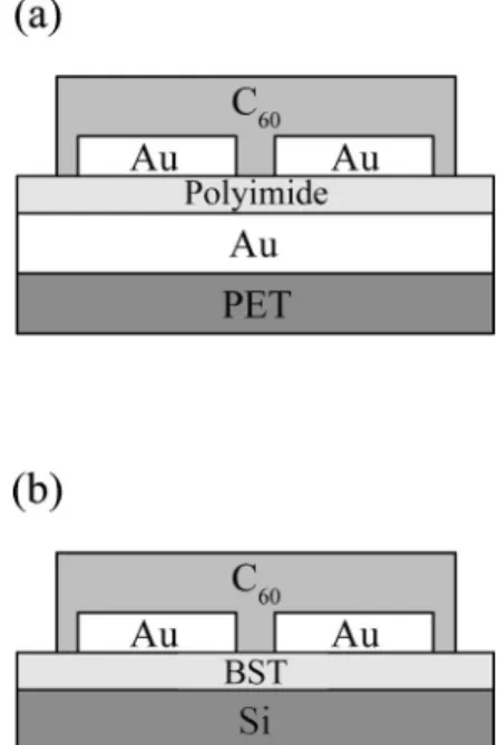
Schematic representations of cross-sectional views of the C60FET devices with polyimide and BST gate insulators are shown in Figs. 1共a兲 and 1共b兲, respectively. Commercially available PET substrate was cleaned by washing with ac-etone, 2-propanol, and ultrapure water, and was dried at 190 ° C. The Au gate electrodes with thickness of 50 nm were formed on the PET substrate by a thermal deposition under vacuum of 10−8Torr. The films of the polyimide gate insulator were formed by a spin coating of a high-purity a兲Electronic mail: [email protected]
APPLIED PHYSICS LETTERS 87, 143506共2005兲
0003-6951/2005/87共14兲/143506/3/$22.50 87, 143506-1 © 2005 American Institute of Physics
polyimide precursor共KEMITITE CT4112, Kyocera Chemi-cal兲 on the Au/PET substrate at 2000 rpm for 5 s and 4000 rpm for 20 s. The films were heated at 100 ° C for 10 min and at 180 ° C for 1 h. The surface of polyimide films was treated to be hydrophobic with hexamethyldisila-zane 共HMDS兲. Fifty 共50兲 nm thickness of Au source-drain electrodes and 150 nm thickness of C60 thin films were formed on the substrate by the thermal deposition under 10−8Torr. The channel length L and the channel width W of the C60FET device with a polyimide gate insulator were 30 and 2000m, respectively.
The BST layer of the chemical composition Ba0.4Sr0.6Ti0.96O3 was fabricated on the As-doped Si 共100兲 wafer 共= 0.001– 0.004⍀ cm兲 by the sol-gel method; the isoamyl acetate-amyl alcohol solution of 7 wt % Ba0.4Sr0.6Ti0.96O3 was purchased from Mitsubishi Materials Corporation. The Si wafer was cleaned by washing with ac-etone, methanol, and H2SO4/ H2O2共4:1 in volume兲, and na-tive SiO2 on the Si wafer was removed by immersing it in dilute HF solution. The wafer was finally washed by ultra-pure water. The precursor film of BST was prepared by a spin coating of the Ba0.4Sr0.6Ti0.96O3solution on the Si strate at 500 rpm for 3 s and at 2000 rpm for 20 s. The sub-strate was prebaked at 300– 400 ° C for 10 min. The spin coating and prebaking were repeated four times before the annealing. The substrate was annealed at 700 ° C for 1 h un-der 100 ml min−1 flow of O
2. Fifty 共50兲 nm thickness of source/drain Au electrodes and 150 nm thickness of C60thin films were formed on the BST/Si substrate by thermal depo-sition under 10−8Torr; the C60 FET device with the BST layer treated by HMDS has also been fabricated. The L and
W of the C60FET device with a BST gate insulator were 30 and 1000m, respectively. The FET properties for all FET devices fabricated in the present study were measured after an annealing at 100– 140 ° C for 24 h under 10−6Torr.
The drain current ID versus VDSplots for the C60 thin-film FET with a polyimide gate insulator at 300 K are shown in Fig. 2共a兲. The plots show n-channel normally off FET properties. The plot of IDversus VGat VDS= 20 V is shown in
Fig. 2共b兲. The IDincreases with increasing VGto positive up
to 100 V. The and the threshold voltage, VT, were
deter-mined to be 7.1⫻10−3 cm2V−1s−1 and 7 V, respectively, from the ID– VG plot with the relation, ID=共WC0/ L兲共VG
− VT兲VDS, where C0 is the capacitance per area.17 The C0 value was determined to be 1.1⫻10−9F cm−2 from the ex-perimental capacitance, C共=C0S兲 measured with an LCR meter, where S is the area of electrode. Further, theand VT
values of the C60FET with the polyimide gate insulator were estimated to be 1.2⫻10−2 cm2V−1s−1and 2 V, respectively, from the 共IDsat兲1/2− VG plot 关Fig. 2共c兲兴 with the relation
共IDsat兲1/2=共WC0/ 2L兲1/2共VG− VT兲 共Ref. 17兲; the saturation of
IDis clearly observed in Fig. 2共a兲. The 共ID
sat兲1/2− V
Gplot was
obtained at VDS of 100 V, and the current on-off ratio,
ID共VG= 100 V兲/ID共VG= 0 V兲, was 160.
The atomic force microscope共AFM兲 image of the poly-imide surface is shown in Fig. 2共d兲. The maximum depth,
Dmax, from the surface of the polyimide layer was 5.5 nm. The thickness, d, of polyimide was estimated to be 3.0m from the C0 value of 1.1⫻10−9F cm−2 with the relation
C0=0x/ d by assuming x of 3.8 共Ref. 14兲, where 0 is permittivity in vacuum. The d value of the polyimide layer in this device is larger by 7 times than that, 420 nm, of the SiO2 layer used by our group in the fullerene FET devices.9–12The value of C0in the C60FET with 420 nm of SiO2layer can be estimated to be⬃8.2⫻10−9F cm−2with C
0=0x/ d asxof
the SiO2layer is 3.9. Therefore, the C0value of the polyim-ide, 1.1⫻10−9 F cm−2, is smaller than that of SiO
2, 8.2 ⫻10−9F cm−2. This implies that the carrier density N共=
C0VG/ e兲, which can be induced at the same VG, is smaller in
the C60FET with a polyimide gate insulator than that with a SiO2 layer. This problem can be solved by fabricating the C60 FET device with a thinner polyimide layer with high quality.
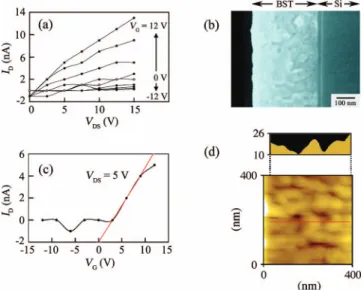
The plots of IDversus VDSfor the C60 FET device fab-ricated with the crystalline BST layer are shown in Fig. 3共a兲. The plots show substantially n-channel normally off enhancement-type properties. The IDincreased with
increas-ing the VG, while at VG= 0 V the ID was extremely small.
When decreasing VGto the negative value, the small IDwas
FIG. 1. Schematic representations of cross-sectional view of C60FET de-vices with a共a兲 polyimide gate insulator and 共b兲 BST gate insulator.
FIG. 2. 共Color兲 共a兲 ID− VDS plots, 共b兲 ID− VGplot at VDS= 20 V, and 共c兲 共ID兲1/2− VGplot at VDS= 100 V for the C60FET with polyimide gate
insula-tor.共d兲 AFM image of the polyimide surface 共bottom兲; the cross-sectional AFM image共top兲 observed along the red line. The brightness in the AFM image共bottom兲 refers to the unevenness of the surface. As the color bright-ens, the part is closer to the surface.
143506-2 Kubozono et al. Appl. Phys. Lett. 87, 143506共2005兲
further reduced owing to the depletion of electrons in the channel region. The value of d for the layer was estimated to be 380 nm from the cross-sectional image of the scanning electron microscope共SEM兲 关Fig. 3共b兲兴. Theand VTvalues
of the FET device were determined to be 4.1 ⫻10−5cm2V−1s−1 and 3 V, respectively, from the I
D− VG
plots 关Fig. 3共c兲兴 at VDS= 5 V with the relation, ID=
共WC0/ L兲共VG− VT兲VDS 共Ref. 17兲. The C0 value was esti-mated to be 8.3⫻10−8F cm−2from the experimental C. The
value estimated for the FET device is much lower than those, 0.08– 0.56 cm2V−1s−1, of the C
60FETs with the SiO2 insulating layer.1,3,4Nevertheless, it should be noted that the
VDSand VGvalues for the FET operation are smaller by one
order of magnitude than those for the C60FET with the SiO2 gate insulator. This result is based on the fact that the high concentration of carriers can be injected even at low VG
ow-ing to the highxgate insulator; the N in the C60/ BST FET is 5.2⫻1012cm−2 at V
G= 10 V, which is comparable to that
in the C60/ SiO2FET at VG= 100 V, 5.1⫻1012cm−2. The low
value can be attributed to a large roughness in the surface of the BST layer. The value of Dmaxfor the BST surface can be estimated to be⬃35 nm from the AFM image shown in Fig. 3共d兲; the BST layer was prepared by one-time annealing. Such a large roughness should suppress the carrier transport. The size of crystallite of the BST was estimated to be 20 nm from the x-ray diffraction peak ascribable to 100 reflection, and the size increased with an increase in annealing time at 700 ° C. As the Dmaxdecreased with an increase in annealing time, the increase in the annealing time may have caused the improvement of carrier transport.
The hydrophobic treatments of the BST thin films were carried out by immersing those into HMDS for 24 h at
300 K. The AFM showed the Dmaxof 10 nm for the HMDS-treated BST surface. The water contact angle increased from 15° to 60° by the HMDS treatment, showing that the BST surface changed to a hydrophobic situation. The ID− VDS
plots showed the n-channel properties with the and VT
values of 1.1⫻10−4cm2V−1s−1 and −5 V, respectively. This shows clearly that the hydrophobic BST surface can increase the value, although the origin remains to be clarified.
In summary, the flexible C60FET device, which exhibits
n-channel normally off properties, has been fabricated with a
polyimide gate insulator on the PET substrate. Furthermore, the C60 FET device, which operates at low VGand VDS, has
been fabricated with the high x gate insulator, BST. The
FET device also showed n-channel FET properties. These should open a way towards high-performance fullerene FET devices exhibiting flexibility, portability, and low-voltage op-eration, and a way towards modification of electronic struc-ture of C60 by high-carrier injection, i.e., a realization of novel physical properties.
This work was partly supported by the Mitsubishi Foun-dation and a Grant-in-Aid共No. 15350089兲 from the Ministry of Education, Culture, Sports, Science and Technology, Japan.
1R. C. Haddon, A. S. Perel, R. C. Morris, T. T. M. Palstra, A. F. Hebard,
and R. M. Fleming, Appl. Phys. Lett. 67, 121共1995兲.
2R. C. Haddon, J. Am. Chem. Soc. 118, 3041共1996兲.
3S. Kobayashi, T. Takenobu, S. Mori, A. Fujiwara, and Y. Iwasa, Appl.
Phys. Lett. 82, 4581共2003兲.
4T. Kanbara, K. Shibata, S. Fujiki, Y. Kubozono, S. Kashino, T. Urisu, M.
Sakai, A. Fujiwara, R. Kumashiro, and K. Tanigaki, Chem. Phys. Lett. 379, 223共2003兲.
5E. Kuwahara, Y. Kubozono, T. Hosokawa, T. Nagano, K. Masunari, and
A. Fujiwara, Appl. Phys. Lett. 85, 4765共2004兲.
6A. Dodabalapur, H. E. Katz, L. Torsi, and R. C. Haddon, Science 269,
1560共1995兲.
7E. J. Meijer, D. M. De Leeuw, S. Setayesh, E. van Veenendaal, B.-H.
Huisman, P. W. M. Blom, J. C. Hummelen, U. Scherf, and T. M. Klapwijk, Nat. Mater. 2, 678共2003兲.
8S. Kobayashi, S. Mori, S. Iida, H. Ando, T. Takenobu, Y. Taguchi, A.
Fujiwara, A. Taninaka, H. Shinohara, and Y. Iwasa, J. Am. Chem. Soc. 125, 8116共2003兲.
9Y. Kubozono, Y. Rikiishi, K. Shibata, T. Hosokawa, S. Fujiki, and H.
Kiatagawa, Phys. Rev. B 69, 165412共2004兲.
10K. Shibata, Y. Kubozono, T. Kanbara, T. Hosokawa, A. Fujiwara, Y. Ito,
and H. Shinohara, Appl. Phys. Lett. 84, 2572共2004兲.
11T. Nagano, H. Sugiyama, E. Kuwahara, R. Watanabe, H. Kusai, Y.
Kashino, and Y. Kubozono, Appl. Phys. Lett. 87, 023501共2005兲.
12T. Nagano, E. Kuwahara, T. Takayanagi, Y. Kubozono, and A. Fujiwara,
Chem. Phys. Lett. 409, 187共2005兲.
13P. R. L. Malenfant, C. D. Dimitrakopoulos, J. D. Gelorme, L. L. Kosbar, T.
O. Grahama, A. Curioni, and W. Andreoni, Appl. Phys. Lett. 80, 2517 共2002兲.
14Y. Kato, S. Iba, R. Teramoto, T. Sekitani, T. Someya, H. Kawaguchi, and
T. Sakurai, Appl. Phys. Lett. 84, 3789共2004兲.
15S.-M. Kang and Y. Leblebici,
CMOSDigital Integrated Circuits, Analysis
and Design共McGraw Hill, New York, 2003兲.
16M. S. Dresselhaus, G. Dresselhaus, and R. C. Eklund, Science of
Fullerenes and Carbon Nanotubes共Academic, San Diego, 1996兲.
17S. M. Sze, Semiconductor Devices, Physics and Technology共Wiley, New
York, 2002兲. FIG. 3. 共Color兲 共a兲 ID− VDS plots, 共b兲 cross-sectional SEM image, 共c兲
ID− VGplot at VDS= 5 V for the C60FET device with BST gate insulator.共d兲
AFM image of the BST surface共bottom兲; the cross-sectional AFM image 共top兲 observed along the red line. In 共a兲, the open circles refer to the ID− VDSplots at VG= 0 V. The brightness in the AFM image共bottom兲 refers to the unevenness of the surface. As the color brightens, the part is closer to the surface.
143506-3 Kubozono et al. Appl. Phys. Lett. 87, 143506共2005兲