第 1 章 序論
5
第 1 章 序論 6 表 1-2 ア プ リ ケ ー シ ョ ン に 適 用 検 討 さ れ て い る プ リ ン テ ッ ド エ レ ク ト ロ ニ ク ス 技 術 7) 印刷方式 カラーフィルタ インクジェット、ロール印刷 アライメントレイヤー インクジェット、グラビア 液晶材料 インクジェット、グラビア スペーサ インクジェット、ロール印刷 配線 印刷全般 TFT背面板 印刷全般、ナノインプリント 配線 インクジェット 電気シールド スクリーン印刷 基板 スロットコーティング、インクジェット
Light emitting layer インクジェット、ノズル
TFT背面板 印刷全般、ナノインプリント 封止 インクジェット 透明電極層 インクジェット、スクリーン印刷 FED Electron emission gap インクジェット E-paper TFT背面板 印刷全般、ナノインプリント LED 透明電極 インクジェット、スクリーン印刷 OLED 有機膜 印刷全般 RFID アンテナ スクリーン印刷、ロール印刷 その他 スクリーン印刷、ロール to ロール Smart ID ディスプレイ ロール印刷、インクジェット Energy 一次電池、二次電池 ロール印刷、ナノインプリント コンデンサ、太陽電池 Packaging センサー インクジェット、ロール印刷、スクリーン 印刷 ナノインプリント センサーモジュール ナノインプリント 通信モジュール ナノインプリント 光学素子 光学素子(回析光学素 子) ナノインプリント LED LED(光取り出し効率向 上) ナノインプリント 単分子検出(SERS; Surface ナノインプリント
第 1 章 序論
17
述 べ る .
第 1 章 序論 18 参 考 文 献 1) 独 立 行 政 法 人 新 エ ネ ル ギ ー・産 業 技 術 総 合 開 発 機 構 ,“プ リ ン テ ッ ド エ レ ク ト ロ ニ ク ス 技 術 に 係 わ る 調 査 ”, 平 成 22年 2月 . 2) 下 田 達 也 , “マ イ ク ロ 液 体 か ら 直 接 に 薄 膜 デ バ イ ス を 形 成 す る 技 術 -マ イ ク ロ 液 体 プ ロ セ ス - ”, ま て り あ , 44, pp.510–517 (2005). 3) 酒 井 真 理, “イ ン ク ジ ェ ッ ト 法 に よ る 回 路 基 板 製 造 技 術 ”, 電 子 情 報 通 信 学 会 誌 , 90, pp.544–548 (2007).
4) M. Singh, H. M. Haverinen, P. Dhagat, and G. E. Jabbour, “Inkjet printing-process and its applications”, Adv. Mater., 22, pp. 673–685, 2010. 5) 富 士 キ メ ラ 総 研, “2018 フ レ キ シ ブ ル / 有 機 / プ リ ン テ ッ ド エ レ ク ト ロ ニ ク ス の 将 来 展 望”, 平 成 30年 1月 . 6) 独 立 行 政 法 人 新 エ ネ ル ギ ー・産 業 技 術 総 合 開 発 機 構 ,“ 次 世 代 プ リ ン テ ッ ド エ レ ク ト ロ ニ ク ス 材 料 ・ プ ロ セ ス 基 盤 技 術 開 発 (中 間 評 価 )” , 平 成 27年 10月 5日 7) 国 立 研 究 開 発 法 人 新 エ ネ ル ギ ー・産 業 技 術 総 合 開 発 機 構 ,“情 報 収 集 事 業 フ レ キ シ ブ ル デ バ イ ス の 用 途 と 技 術 課 題 等 に 関 す る 調 査” (2016).
8) B. Derby, “Inkjet Printing of Functional and Structural Materials: Fluid Property Requirements, Feature Stability, and Resolution” , Annu. Rev. Mater. Res. , 40, pp.395–414 (2010).
9) K. Fukuda, T. Sekine, D. Kumaki, and S. Tokito, “Profile Control of Inkjet Printed Silver Electrodes and Their Application to Organic Transistors”, ACS applied materials & interfaces, 5, pp.3916-3920 (2013).
第 1 章 序論
19
Flexible Substrate for OLED Applications”, J. Phys. Chem. C, 113, pp. 13398–13402 (2009).
11) R. D. Deegan, O. Bakajin, T. F. Dupont, G. Huber, S. R. Nagel, and T. a Witten, “Capillary flow as the cause of ring stains from dried liquid drops”, Nature, 389, pp.827–829 (1997).
12) D. Soltman and V. Subramanian, “Inkjet -printed line morphologies and temperature control of the coffee ring effec t”, Langmuir, 24, pp.2224–2231 (2008).
13) B. J. De Gans and U. S. Schubert, “Inkjet printing of well -defined polymer dots and arrays”, Langmuir, 20, pp.7789–7793 (2004).
14) D. Espalin, D. W. Muse, E. Macdonald, and R. B. Wicker, “3D Printing multifunctionality : structures with electronics”, Int J AdvManuf Technol, 72, pp.963–978 (2014).
15) “筐 体 一 体 型 配 線 技 術 ”, 東 芝 レ ビ ュ ー , 64, p.45 (2009).
第 2 章 低エネルギーイメージングデバイス及び照明デバイス 21 電 子 を 放 出 さ せ , さ ら に エ ミ ッ タ と ア ノ ー ド 間 に 電 界 を 印 加 す る こ と で , ア ノ ー ド に 電 子 を 照 射 す る こ と が で き る . PdO ナ ノ 膜 に ジ ュ ー ル 熱 で 形 成 す る ギ ャ ッ プ を 低 電 力 で ,か つ 電 極 間 に 均 一 に 形 成 す る に は , PdO ナ ノ 膜 が 電 極 間 で 高 抵 抗 か つ 幅 方 向 に 抵 抗 値 が 揃 っ て い る こ と が 重 要 で あ る . そ の た め , PdO ナ ノ 膜 は 薄 く 均 一 な 膜 厚 で 形 成 す る 必 要 が あ る . 図 2-2 に PdO ナ ノ 膜 の 断 面 形 状 の 概 略 を 示 す . 膜 の 断 面 形 状 を 定 量 化 す る た め , 凹 凸 率 F (%) を 式 (2-1) に 示 す 計 算 式 に よ り 算 出 し た .
100
1
2
−
+
=
R L ct
t
t
F
(2-1) tL (nm), tR (nm) は ,そ れ ぞ れ 端 部 か ら 5 m 内 側 の 範 囲 に お け る 左 側 と 右 側 の 最 大 膜 厚 を 示 す . tc (nm) は 中 央 部 の 膜 厚 で あ る . F が マ イ 図 2-1 PdO ナ ノ 膜 を 用 い た 平 面 型 電 界 エ ミ ッ タ の 概 略PdO based emitter
Electrode
Anode
Electron
Gap
第 2 章 低エネルギーイメージングデバイス及び照明デバイス
28
参 考 文 献
1) Y. Honda, M. Nanba, K. Miyakawa, M, Kubota, M. Nagao, Y. Neo, H. Mimura and N. Egami,“Electrostatic-focusing image sensor with volcano-structured Spindt -type field emitter array”, J. Vac. Sci. Technol. B, Nanotechnol. Microelectron. Mater. Process. Meas. Phenom., 34, p.52201 (2016).
2) 後 藤 康 仁,“ フ ィ ー ル ド エ ミ ッ タ ア レ イ の 新 し い 応 用 技 術 ~ 耐 熱 ・ 耐 放 射 線 素 子 や 光 源 応 用 に 向 け て ~”, J. Vac. Soc. Jpn., 60, pp.25–33 (2017).
3) W. B. Hu, Y. L. Sun, and S. L. Wu,“Electron Emission Properties of Surface-Conduction Electron Emitters With a PdO-C-PdO Multilayer Conductive Film Deposited by Magnetron Sputtering”, Journal of electronic materials , 40, pp.2020–2026(2011).
4) C. H. Tsai, F. M. Pan, K. J. Chen, C. Y. Wei, M. Liu, and C. N. Mo, “Nanogap formation by palladium hydrogenation for surface conduction electron emitters fabrication Nanogap formation by palladium hydrogenation for surface conduction electron emitters fabrication”, Applied physics letters, 163115, pp.2005–2008 (2014). 5) S.Itoh, M. Tanaka, T. Tonegwa, M . Taniguchi, K. Otsu, T. Niiyama, K.
Tamura, M. Namikawa, Y. Naito, Y. Obara, M. Toriumi, M. Kitada, Y .Takeya, K. Deguchi, S. Kawata, Y. Sato, F. Kataoka, H. Toki, K. Sakurada, and T. Yamaura, “Development of field -emission displays Related content”, J. Soc. Inf. Disp., 15, pp.1057–1064 (2007).
6) M. Okuda, S. Matsutani, and A. Asai, “Electron trajectory analysis of surface conduction electron emitter displays”, SID Symp. Dig., 29, pp.185–188 (1998).
第 2 章 低エネルギーイメージングデバイス及び照明デバイス
29
Hatanaka, “71.1: Invited Paper: A 36-inch Surface-conduction Electron-emitter Display (SED)”, SID 05 Dig. Tech. Pap., 36, pp.1929–1931 (2005).
8) K. Yamamoto, T. Oguchi, K. Sasaki, I. Nomura, S. Uzawa, and K. Hatanaka, “Fabrication and characterization of surface-conduction electron emitters for SED application”, J. Soc. Inf. Disp., 14, p.73 (2006).
9) K. Yamamoto, S. Takagi, T. Moriguchi, and Y. Kataoka, “Characterization of Carbon Nano-Gap for Surface Conduction Electron Emitters”, Jpn. J. Appl. Phys., 48, 122201.
10) Y. Li and H. Lo, “Surface conduction electron emission in palladium hydrogenation nanogaps”, Journal of Physics D: Applied Physics, 41, 085301 (2008).
11) B. R. H Fowler and L. Nordheim, “Electron Emission in Intense Electric Fields”, Phys. Rev. Proc. Nat. Ac. Sci.Roy. Soc. Proc. Z. f. Phys., 14, pp.80–51 (1923).
12) G. A. K. and M. E. C. M.I.Elinson, A.G.Zhdan, “E mission of Hot Electrons and Field Emission of Electrons from Tin Oxide”, RADIO Eng. Electron. PHYSICS -USSR, 10, p.1290(1965).
13) G. Dittmer, “Electrical conduction and electron emission of discontinuous thin films”, Thin Solid Films, 9, pp.317–328 (1972). 14) M. Hartwell and C. G. Fonstad, “Strong electron emission from
patterned tin-indium oxide thin films”, International Electron Devices Meeting, 21, pp.519–521 (1975).
15) H. Araki and T. Hanawa, “Electroforming of a carbon thin film device with a silver film”, Thin Solid Films, 152, pp.481–486 (1987).
第 2 章 低エネルギーイメージングデバイス及び照明デバイス
30
ギ ャ ッ プ 形 成 機 構 に 関 す る 研 究”, 東 北 大 学 (2010).
17) M. R. Krames, O. B. Shchekin, R. Mueller -Mach, G. O. Mueller, L. Zhou, G. Harbers, M. G. Craford, “Status and future of high -power light-emitting diodes for solid -state lighting”, J. Disp. Technol., 3, pp.160–175 (2007).
18) A. Aboulaich, M. Michalska, R. Schneider, A. Potdevin, J. Deschamps, R. Deloncle, G. Chadeyron, R. Mahiou, “Ce-doped YAG nanophosphor and red emitting CuInS2/ZnS core/shell quantum dots for warm white light -emitting diode with high color rendering index”, ACS Appl. Mater. Interfaces , 6, pp.252–258, (2014).
19) C. Sun, Y. Zhang, Y. Wang, W. Liu, S. Kalytchuk, S. V. Kershaw, T. Zhang, X. Zhang, J. Zhao, W. W. Yu, A. L. Rogach, “High color rendering index white light emitting diodes fabricated from a combination of carbon dots and zinc copper indium sulfide quantum dots”, Appl. Phys. Lett., 104, p.261106 (2014).
20) C. H. Chiang, S. J. Gong, T. S. Zhan, K. C. Cheng, and S. Y. Chu, “White Light-Emitting Diodes with High Color Rendering Index and Tunable Color Temperature Fabricated Using Separated Phosphor Layer Structure”, IEEE Electron Device Lett., 37, pp.898–901 (2016). 21) J. K. Sheu, S. J. Chang, C. H. Kuo, Y. K. Su, L .W. Wu, Y .C. Lin, W. C. Lai, J. M. Tsai, G .C. Chi, R. K. Wu, “White -light emission from near UV InGaN-GaN LED chip precoated with blue/green/red phosphors”, IEEE Photonics Technol. Lett., 15, pp.18–20 (2003). 22) T. Nishida, T. Ban, and N. Kobayashi, “High -color-rendering light
第 2 章 低エネルギーイメージングデバイス及び照明デバイス
31
23) W.-R. Liu, C.-H. Huang, C.-P. Wu, Y.-C. Chiu, Y.-T. Yeh, and T.-M. Chen, “High efficiency and high color purity blue -emitting NaSrBO3:Ce3 + phosphor for near-UV light-emitting diodes”, J. Mater. Chem., 21, p.6869 (2011).
24) J. Weibel, T. Basishvili, M. Dattler, C. Garbazza, F. Rudzik, C. Renz, and C. Cajochen, “Effect of a daylight LED versus a conventional LED solution on visual comfort, daytime alertness and sleep”, Sleep,
40, Issue suppl_1, 28 April 2017, p.A61.
25) J. K. Kim, H. Luo, E. F. Schubert, J. Cho, C. Sone, and Y. Park, “Strongly enhanced phosphor efficiency in GaInN white light-emitting diodes using remote phosphor configuration and diffuse reflector cup”, Japanese J. Appl. Physics, Part 2 Lett., 44, pp.13–16 (2005).
26) M. Dal Lago, M. Meneghini, N. Trivellin, G. Mura, M. Vanzi, G. Meneghesso, E. Zanoni, “Phosphors for LED -based light sources: Thermal properties and reliability issues”, Microelectron. Reliab., 52, pp.2164–2167 (2012).
27) H. T. Huang, Y. P. Huang, and C. C. Tsai, “Planar lighting system using array of blue leds to excite yellow remote phosphor film”, J. Disp. Technol., 7, pp.44–51 (2011).
28) M. Meneghini, M. Dal Lago, N. Trivellin, G. Meneghesso, and E. Zanoni, “Thermally activated degradation of remote phosphors for application in LED lighting”, IEEE Trans. Device Mater. Reliab., 13, pp.316–318 (2013).
第 2 章 低エネルギーイメージングデバイス及び照明デバイス
32
(2006).
30) M. Conner, “Remote phosphor expands reach of LED light”, https://www.edn.com/design/led/4369591/Remote -phosphor-expands-reach-of-LED-light (March 17, 2011).
31) LeadLite Inc.ホ ー ム ペ ー ジ , http://leadlightinc.com/led/lighting/. 32) Z. Liu, K. Wang, X. Luo, S. Liu, “Realization of high spatial color
uniformity for white light -emitting diodes by remote hemispherical YAG: Ce phosphor film”, in Proc. Electron. Components Technol. Conf., 2010, pp. 1703 –1707.
33) Z. Y. Liu, S. Liu, K. Wang, X. B. Luo, “Studies on optical consistency of white LEDs affected by phosphor thickness and concentration using optical simulation”, IEEE Trans. Components Packag. Technol., 33, pp. 680–687 (2010).
第3 章 湿度調整によるドット状膜の形状再形成プロセス
43
図 3-6 ピ ニ ン グ 材 添 加 に よ る 液 滴 の 縮 退 率 の 変 化
第3 章 湿度調整によるドット状膜の形状再形成プロセス
59
参 考 文 献
1) K. Fukuda, T. Sekine, D. Kumaki, and S. Tokito, “Profile Control of Inkjet Printed Silver Electrodes and Their Application to Organic Transistors”, ACS applied materials & interfaces, 5, pp.3916-3920 (2013).
2) F. Villani, P. Vacca, G. Nenna, O. Valentino, G. Burrasca, T. Fasolino, C. Minarini, and D. della Sala, “Inkjet Printed Polymer Layer on Flexible Substrate for OLED Applications”, J. Phys. Chem. C, 113, pp. 13398–13402 (2009).
3) R. D. Deegan, O. Bakajin, T. F. Dupont, G. Huber, S. R. Nagel, and T. a Witten, “Capillary flow as the cause of ring stains from dried liquid drops”, Nature, 389, pp.827–829 (1997).
4) R. D. Deegan, O. Bakajin, T. F. Dupont, G. Huber, S. R. Nagel, and T. A. Witten, “Contact line deposits in an evaporating drop”, Phys. Rev. E, 62, pp.756–765 (2000).
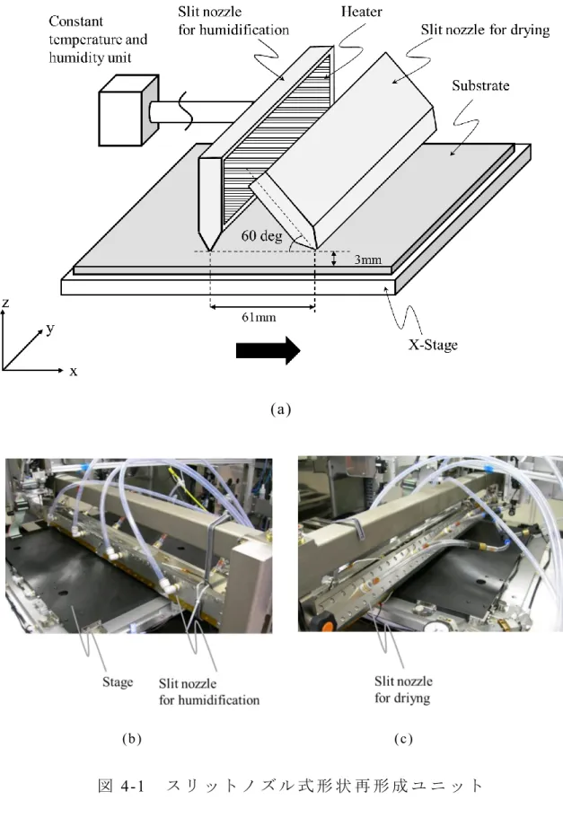
第4 章 スリットノズル式形状再形成プロセス
63
(a)
(b) (c)
第4 章 スリットノズル式形状再形成プロセス
73
図 4-6 空 気 線 図
第4 章 スリットノズル式形状再形成プロセス
80
参 考 文 献
1) D.SONNTAG, “Advancements in the field of hygrometry”, Meteorol. Zeitschrift, 3, pp. 51–66 (1994).
2) Y. T. Gizachew, L.Escoubas, J. J. Simon, M. Pasquinelli, J. Loiret, P. Y. Leguen, J. C. Jimeno, J. Martin, A. Apraiz, and J. P. Aguerre, “Towards ink-jet printed fine line front side metallizat ion of crystalline silicon solar cells ”, Solar Energy Materials and Solar Cells, 95, S70 (2011).
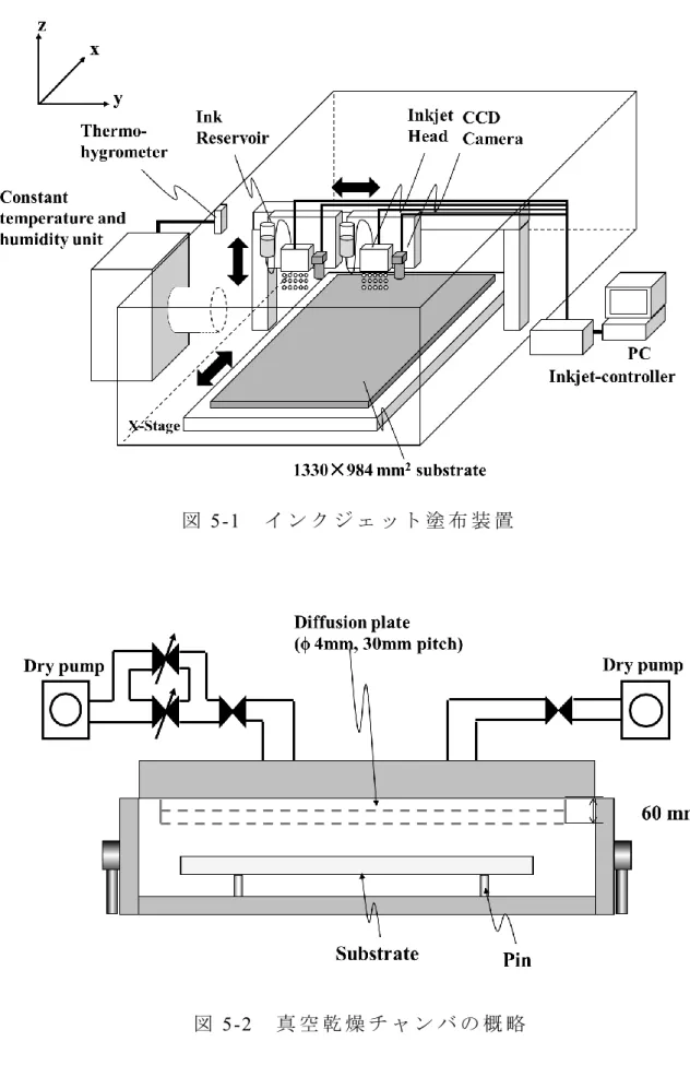
第5 章 大型基板用スリットノズル式形状再形成プロセス
82
図 5-1 イ ン ク ジ ェ ッ ト 塗 布 装 置
第5 章 大型基板用スリットノズル式形状再形成プロセス
83
第5 章 大型基板用スリットノズル式形状再形成プロセス
84
第5 章 大型基板用スリットノズル式形状再形成プロセス
89
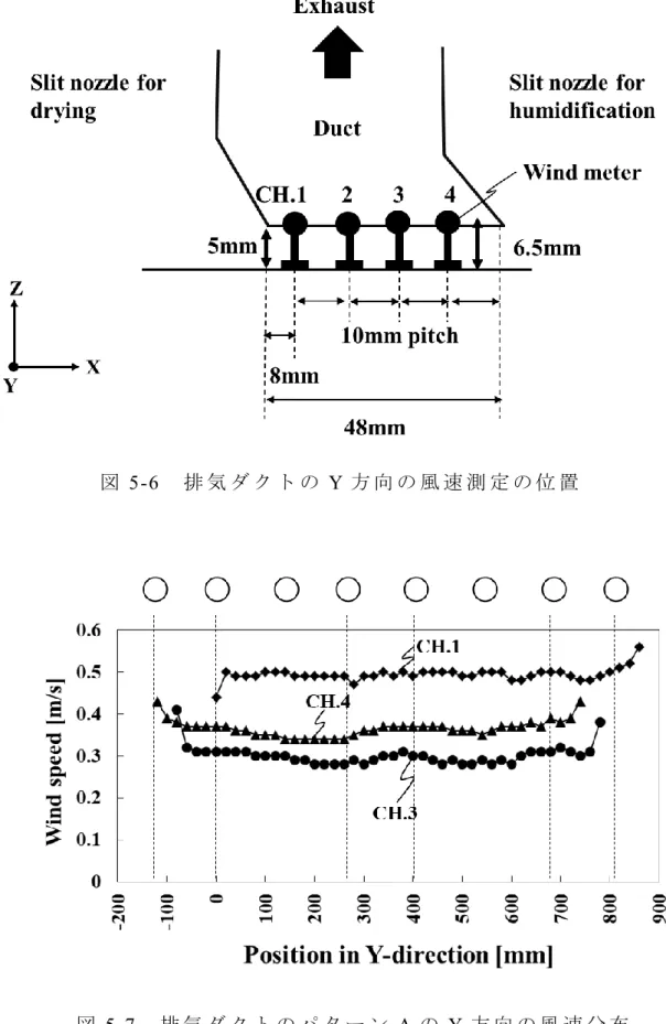
図 5-6 排 気 ダ ク ト の Y 方 向 の 風 速 測 定 の 位 置
第5 章 大型基板用スリットノズル式形状再形成プロセス
90
図 5-8 排 気 ダ ク ト の パ タ ー ン B の Y 方 向 の 風 速 分 布
第6 章 立体内面への均一塗布プロセス 104 6. 2 装 置 の 構 成 と 実 験 方 法 蛍 光 体 グ ロ ー ブ は , グ ロ ー ブ の 内 部 に 蛍 光 体 粉 末 と 熱 硬 化 性 シ リ コ ー ン 樹 脂 を 混 合 し た 蛍 光 体 ス ラ リ ー を 塗 布 し , 加 熱 す る こ と で 蛍 光 体 ス ラ リ ー を 硬 化 さ せ て 蛍 光 体 層 を 形 成 す る .図 6-2 に 蛍 光 体 ス ラ リ ー の 塗 布 装 置 を 示 す . グ ロ ー ブ を 固 定 す る チ ャ ッ ク と , そ の チ ャ ッ ク を 自 公 転 さ せ る た め の 自 転 軸 と 公 転 軸 を 備 え て い る . 自 転 軸 と 公 転 軸 は モ ー タ ー に 接 続 さ れ て お り , そ れ ぞ れ 独 立 に 2000 rpm ま で 調 整 で き る . 自 転 と 公 転 の 回 転 数 を 変 え る こ と に よ っ て , グ ロ ー ブ 内 に 滴 下 し た 蛍 光 体 ス ラ リ ー に 加 わ る 遠 心 力 の 向 き と 大 き さ を 調 整 す る こ と で , グ ロ ー ブ の 内 面 に 蛍 光 体 ス ラ リ ー を 塗 り 広 げ る こ と が で き る . グ ロ ー ブ の 内 面 へ 蛍 光 体 ス ラ リ ー を 滴 下 し や す く す る た め ,自 転 軸 は 公 転 軸 に 対 し て ,45傾 け て い る . ま た , 公 転 に よ る 遠 心 力 を 調 整 す る た め に , 自 転 軸 の 長 さ X を 調 整 す る こ と が で き る . 回 転 中 の グ ロ ー ブ を 加 熱 し な が ら 塗 布 す る た め に , 回 転 部 を 覆 う よ う に 加 熱 ユ ニ ッ ト (ヒ ー タ 温 度 180°C) を 設 置 で き る . 蛍 光 体 ス ラ リ ー の 塗 布 後 , 塗 布 し た グ ロ ー ブ は オ ー ブ ン (ヤ マ ト 科 学 製 DKN402) に て 100°C, 1 時 間 の 大 気 雰 囲 気 で 硬 化 さ せ た . 塗 布 す る 蛍 光 体 ス ラ リ ー は ,透 明 な シ リ コ ー ン 樹 脂 (信 越 化 学 製 KJ R-9022) と 青 ,黄 ,赤 の 蛍 光 体 で 構 成 さ れ て い る .青 ,黄 ,赤 の 蛍 光 体 に は そ れ ぞ れ (Sr,Ba,Ca)1 0(PO4)6Cl2:Eu, (Sr,Ba,Mg)2SiO4:Eu,Mn, Sr2Si7Al3ON1 3:Eu を 使 用 し た . ポ リ カ ー ボ ネ ー ト 製 の グ ロ ー ブ に 蛍 光 体 ス ラ リ ー を 塗 布 し た .
第6 章 立体内面への均一塗布プロセス
105
図 6-2 (a) 開 発 し た 自 公 転 塗 布 装 置 と (b) 回 転 部 の 写 真 (b)
第6 章 立体内面への均一塗布プロセス
107
(a)
(b)
第6 章 立体内面への均一塗布プロセス
108
第6 章 立体内面への均一塗布プロセス
111
球 と White-COB を 搭 載 し た LED 電 球 の 全 光 束 ,発 光 効 率 ,配 光 特 性 を 比 較 し た .
第6 章 立体内面への均一塗布プロセス
116
図 6-8 蛍 光 体 層 の 厚 さ に 対 す る 公 転 速 度 の 依 存 性
第6 章 立体内面への均一塗布プロセス
121
図 6-11 蛍 光 体 ス ラ リ ー の 粘 度 の 温 度 依 存 性
第6 章 立体内面への均一塗布プロセス
125
図 6-15 試 作 し た RP-LED 電 球 の 発 光 ス ペ ク ト ル
第6 章 立体内面への均一塗布プロセス
132
参 考 文 献
1) B. T. Chen, “Investigation of the solvent evaporation effect on spin coating of thin films”, Polym. Eng. Sci., 23, pp.399–403 (1983). 2) D. Q. Pi erre -Gi ll es de Gennes, François e Brochard -W yart , Goutt es,
bul l es , perl es et ondes . Beli n (2005).
3) JIS Z 8701, “XYZcolor system and X10Y10Z10 color system ”, 1995.
4) Pai-Yang Tsai, Hou-Kuei Huang, Jian-Min Sung, Ming-Chi Kan, Yeong-Her Wang, "High thermal stability and wide angle of white light chip-on-board package using a remote phosphor structure ”, IEEE Electron Device Letters, 36, pp. 250-252 (Mar. 2015).
5) Xingjian Yu, Bin Xie, Bofeng Shang, Weicheng Shu, and Xiaobing Luo, “A Facile Approach to Fabricate Patterned Surfaces for Enhancing Light Efficiency of COB -LEDs”, IEEE Transactions on Electron Devices, 64, pp. 4149-4155 (Oct. 2017).
6) Xiaobing Luo, Run Hu, Sheng Liu, KaiWang, “Heat and fluid flow in high-power LED packaging and applications ”, Progress in Energy and Combustion Science, 56, pp. 1-32 (2016).
7) Huai Zheng, Lan Li, Xiang Lei, Xingjian Yu, Sheng Liu, Xiaobing Luo, “Optical performance enhancement for chip -on-board packaging LEDs by adding TiO2/silicone encapsulation layer ”, IEEE electron device letters, 35, pp. 1046-1048 (Oct. 2014).
8) Yiting Zhu and Nadarajah Narendran, “Investigation of remote-phosphor white light -emitting diodes with multi -phosphor layers”, Japanese Journal of Applied Physics, 49, 100203 (Oct. 2010).
第6 章 立体内面への均一塗布プロセス
133
Uchida, S. Kurai and T. Taguchi, “Superior illuminant characteristics of color rendering and luminous efficacy in multilayered phosphor conversion white light sources excited by near-ultraviolet light-emitting diodes”, Japanese Journal of Applied Physics, 48, 112101 (Nov. 2009).
10) C. H. Chiang, S. J. Gong, T. S. Zhan, K. C. Cheng, and S. Y. Chu, “White light-emitting diodes with high color rendering index and tunable color temperature fabricated using separated phosphor layer structure”, IEEE Electron Device Letters, 37, pp. 898-901 (Jun. 2016).
11) Jiasheng Li, Zongtao Li, Guanwei Liang, Shudong Yu, Yong Tang, Xinrui Ding, “Color uniformity enhancement for COB WLEDs using a remote phosphor film with two freeform surfaces ”, Optics Express,
24, pp. 23685-23696 (2016).
12) Jiasheng Li, Zongtao, Li, Zhi Li, Yong Tang, Xinrui Ding, Binhai Yu, "Improvement in optical performance and color uniformity by optimizing the remote phosphor caps geometry for chip -on-board light emitting diodes ”, Solid-State Electronics, 126, pp. 36-45 (Dec. 2016).
研究業績
143
研究業績
1. 本研究に関する発表論文 (3 件)
(1) H.Kondo, T.Sato, J.Yamabe and H.Ishikawa, “Novel inkjet printing system and formation mechanism of PdO nanofilms for field-emission imaging devices,” Journal of Physics D: Appl. Phys, 50, 325106 (2017). [本論文第 3 章]
(2) H.Kondo, T.Sato, and H.Ishikawa, “Large-area profile transformation of inkjet-printed Pd precursor films by slit-nozzle humidification and redrying for PdO nanofilm field emitters,” Journal of imaging science technology, DOI:10.2352/J.ImagingSci.Technol.2018.62.4.040501 (in press). [本論文第 4 章]
(3) H.Kondo, and H.Ishikawa, “Formation of coated phosphor layers by rotation-revolution for remote-phosphor LED bulbs and characterization of LED light bulb with super-high color rendition,” IEEE Transactions on Components, Packaging and Manufacturing Technology, DOI:10.1109/TCPMT.2018.2854680 (in press). [本論文第 6 章]
研究業績
144
精密工学会秋季大会学術講演会 (Sep.2018 函館アリーナ). [本論文第 6 章]
3. その他の論文発表等 (4 件)
(1) 近藤弘康, 山内健資, Abdel Fattah Essam, 菅井 秀郎, “表面波プラズマ生 成における窓表面の周期的凹凸の効果 I 実験”, 応用物理学会学術講演 会講演予稿集, 49 (Mar. 2002, 神奈川大学), p.129.
(2) 山内健資,近藤弘康,Abdel Fattah Essam,加納正明,菅井秀郎, “表面波 プラズマ生成における窓表面の周期的凹凸の効果”, 電気学会プラズマ 研究会, PST-02 (Apr. 2002), p.59.
(3) 近藤弘康, 山内健資, “マグネトロンプラズマに対する RF 周波数の影響”, 応用物理学会学術講演会講演予稿集, 63 (Sep. 2002), p.109.