Kyozo TSUJIKAWA††, Kazuhide NAKAJIMA††, Fumihiko YAMAMOTO††,andKunimasa SAITOH†,Members
SUMMARY A PLC based mode multi/demultiplexer based on asym- metric directional coupler has advantages in terms of compactness, mass productivity, low insertion loss, and matured reliability. However, it has relatively large wavelength dependence due to the difference of cou- pling length. To expand the bandwidth, we have designed two-mode (LP01/LP11a) multi/demultiplexer by wavefront matching method and demonstrated the broadband and low-loss characteristics. This paper re- views the device design by wavefront matching method and investigates the mechanism of its broadband characteristics.
key words: WFM method, PLC, MDM, mode multi/demultiplexer
1. Introduction
In order to meet the growing demand for the transmis- sion capacity, mode-division multiplexing (MDM) trans- mission has attracted a lot of attentions[1]. Mode multi/demultiplexer (MUX/DEMUX) is a necessary compo- nent to realize MDM transmission. Mode MUX/DEMUXs based on free-space optics[2], fiber coupler[3]–[5], pho- tonic lanterns[6], and planar lightwave circuit (PLC)[7],[8]
have been proposed. The PLC-based mode MUX/DEMUX has advantages in terms of compactness, low insertion loss, and mass productivity. PLC-based mode MUX/DEMUX based on asymmetric directional coupler (ADC) is sim- ple and often used, however, it has relatively large wave- length dependence because the coupling length depends on wavelength. Large wavelength dependence of mode MUX/DEMUX limits the available bandwidth in the sys- tem, therefore, wavelength insensitive components are strongly desired.
To solve this problem, we have proposed a PLC- based broadband and low-loss two-mode (LP01/LP11a) MUX/DEMUX based on the wavefront matching (WFM) method optimization[9]–[15]. Here, we regard the funda- mental mode (E11mode) in waveguide as LP01mode in the optical fiber, and the first higher mode (E21mode) in wave- guide as LP11amode in the optical fiber. The WFM method needs less computational time and enables us to obtain op-
Manuscript received November 2, 2017.
Manuscript revised February 10, 2018.
∗This is a review article.
†The authors are with the Graduate School of Information Science and Technology, Hokkaido University, Sapporo-shi, 060–
0814, Japan.
††The authors are with the Access Network Service System Laboratories, NTT Corporation, Tsukuba-shi, 305–0805, Japan.
a) E-mail: [email protected] DOI: 10.1587/transele.E101.C.518
timum structure deterministically.
In our previous work[15], numerical results show that, the insersion loss is lower than −0.3 dB in the wavelength range from 1400 to 1700 nm with the pro- posed structure and it has large fabrication tolerance com- pared to the conventional structure. Furthermore, the de- signed structure was fabricated and broadband character- istics are well-reproduced, showing the usefulness of pro- posed MUX/DEMUX.
In this paper, we review the device design based on WFM method and investigate the mechanism why the pro- posed MUX/DEMUX has broadband characteristics. This paper is organized as follows. In Sect. 2, the principle of the WFM method and the optimization procedure of mode MUX/DEMUX is described. In Sect. 3, the design of mode MUX/DEMUX based on the WFM method and the opti- mization parameter dependence are presented. In Sect. 4, the mechanism of broadband characteristics of the WFM- designed device is investigated through a comparison with tapered ADC. The conclusion of this paper is given in Sect. 5.
2. Wavefront Matching Method
PLC-based devices are usually designed by trial and error (human design). It is effective for PLCs to design with fixed geometry and small number of structural parameters by the designer’s original idea, however, the large num- ber of structural parameters makes it difficult to find op- timum solution for PLC. Furthermore, it is hard to get a novel structure, just by changing the structural parameters.
In order to determine the design automatically from desired characteristics, many optimization methods have been de- veloped, such as genetic algorithm[16], topology optimiza- tion[17], and WFM method[9]–[15]. WFM method is an optimization algorithm based on beam propagation method (BPM)[18],[19], which determine the optimum index pro- files from the ideal output field. WFM method has advan- tages such as the fast convergence speed and large calcu- lation flexibility. WFM method has been applied to the waveguide lens[10], Y-branch waveguide[11], waveguide crossing[12], multimode interferometer[13]. The validity and effectiveness have been demonstrated experimentally. It should be noted that WFM method can be applied to opera- tions for higher order modes. The design of mode rotator by WFM method has also been reported[14]. The simulation Copyright c2018 The Institute of Electronics, Information and Communication Engineers
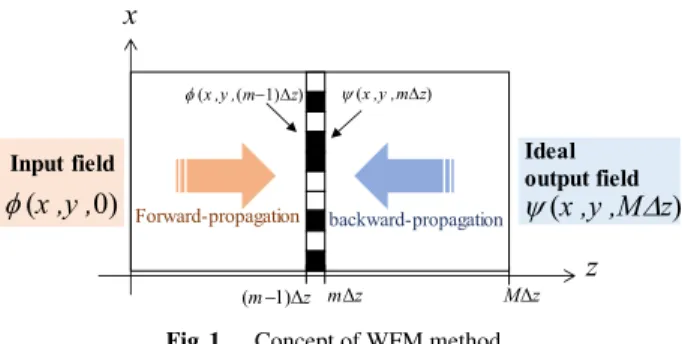
Fig. 1 Concept of WFM method.
results show the optimization for the conversion between LP11a and LP11bmodes without affecting LP01 mode. This proposal suggests the scalability for higher order modes.
Figure 1 shows the concept of the WFM method, where z,φ(x,y,0), andψ(x,y,MΔz) are the propagation direction, the normalized input field, and the normalized ideal output field, respectively. Here, the normalization of the field is done by setting the integration of|φ|2(or|ψ|2) over the cross section of the waveguide to 1. The coupling coefficient η between the propagated input field and the ideal output field at the output port (z=MΔz) is evaluated as
η=
ψ∗(x,y,MΔz)φ(x,y,MΔz)dxdy
2
, (1)
whereφ(x,y,MΔz) is the input field that propagates forward to the output port and the superscript∗represents the com- plex conjugate. By using BPM for the field propagation, φ(x,y,MΔz) is described as
φ(x,y,MΔz)=(ABMA)· · ·(ABmA)· · ·(AB1A)φ(x,y,0), (2) where A is the operator forΔz/2 propagation of the free space, andBmis the phase shift operator atz=mΔz. From Eq. (1) and Eq. (2), the coupling coefficientηat the output port is expressed as
η=
ψ∗(x,y,mΔz)ABmAφ(x,y,(m−1)Δz)dxdy
2
. (3) From Eq. (3), it can be seen that the coupling coefficientη at the output port is evaluated from the overlap integral be- tweenψ∗(x,y,mΔz) that propagates backward tomΔzand φ(x,y,mΔz) that propagates forward tomΔz. This means that the coupling coefficient ηcan be improved by chang- ing the refractive index distribution to match the wavefront ofψ∗(x,y,mΔz) andφ(x,y,mΔz) at every propagation step.
Here,Bmcan be described as
Bm=exp(−jk(nm(x,y)−nref)Δz). (4) nm(x,y),nref, andkare the refractive index distribution at z=mΔz, the reference refractive index, and the wavenum- ber. When the refractive index distribution is changed from nm(x,y) tonm(x,y)+δnm(x,y), the phase shift operatorBm
Fig. 2 Schematic of LP01/LP11aPLC-based mode MUX/DEMUX.
is expressed as
Bm=exp[−jk((nm(x,y)+δnm(x,y))−nref)Δz]
Bm(1−jkδnm(x,y)Δz). (5)
Here, we use approximation assuming kδnm(x,y)Δz 1.
From Eq. (3) and Eq. (5), the coupling coefficient η cor- responding the changed refractive-index distribution is ex- pressed as
η=
ψ∗(x,y,mΔz)ABmAφ(x,y,(m−1)Δz)dxdy
2
ψ∗(x,y,mΔz)ABm(1−jkδnm(x,y)Δz)A
φ(x,y,(m−1)Δz)dxdy
2
η+2kΔzη
δnm(x,y)Im[ψ∗(x,y,mΔz)φ(x,y,mΔz)]dxdy
ψ∗(x,y,mΔz)φ(x,y,mΔz)dx (6) From Eq. (6), it can be seen that if the sign ofδnm(x,y) is the same as Im[ψ∗(x,y,mΔz)φ(x,y,mΔz)], the coupling co- efficient can be improved.
Figure 2 shows a structure of LP01/LP11a PLC-based mode MUX/DEMUX to optimize. When LP01 mode is launched at port 1, it goes through to port 3. When LP01
mode is launched to port 2, it is coupled to LP11a mode in Waveguide 1 by matching the effective indices of LP01
mode of Waveguide 2 and LP11a mode of Waveguide 1.
Three-dimensional scalar finite element beam propagation method (3D-SFE-BPM)[18], [19]is used for WFM opti- mization. For changing the refractive index distribution, we used “solid pattern” approach[10]to avoid large waveguide discontinuity. The WFM optimization is done as follows:
1) Calculate forward transmission spectra of port 2 to port 3 (LP01 input) and port 1 to port 4 (LP11a input) for desired wavelength range.
2) Calculate backward transmission spectra of port 3 to port 2 (LP11a input) and port 4 to port 1 (LP01 input) for desired wavelength range.
3) Obtainηfor above two combinations (port 2 to port 3
3. Design of PLC-Based Mode MUX/DEMUX by WFM Method
3.1 Spectral Change by WFM Optimization
The parameter of PLC isΔ = 0.386%[7]. The waveguide height is h = 6.0 μm, waveguide widths are W1 = 19.2 μm andW2 =7.5μm, the gap between two waveguides is Gap=4.0μm, the coupling length isL = 3.0 mm. In the S-bend part, the separation of both ends isSep=50.0μm, and the S-bend length isLs=3.16 mm. The bend radius of S-bend is 50 mm so that radiation loss can be reduced nearly to zero.
The LP01/LP11a PLC-based mode MUX/DEMUX is optimized by using WFM method with wavelengths from 1300 nm to 1700 nm simultaneously. The cell size is Δx=0.1μm,Δy=0.5μm, andΔz=2.0μm. In general, the bandwidth of a directional coupler is wider for narrower
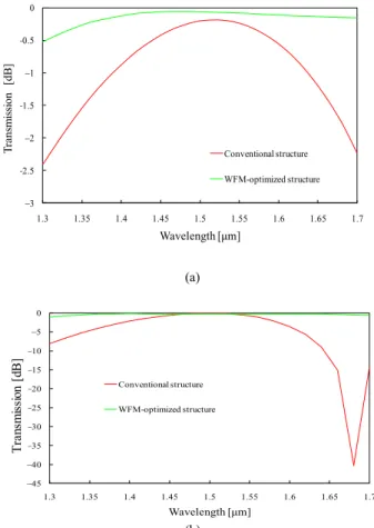
Fig. 3 Transmission spectra of LP11amode from port 2 to port 3.
Fig. 4 Transmission of LP11amode from port 2 to port 3 as a function of iteration.
sertion loss around−12 dB at the wavelengths of 1700 nm.
On the other hand, the blue line in Fig. 3 shows the transmis- sion spectrum of the WFM-optimized structure. The WFM- optimized structure has a flat spectrum and the insertion loss is less than −0.3 dB with wavelengths from 1400 nm to 1700 nm.
Figure 4 shows the transmission of LP11a mode from port 2 to port 3 as a function of calculation count for wave- length of 1.30, 1.50, and 1.70 μm during WFM optimiza- tion. It can be seen that the transmissions are converged by iteration. At 1.70μm, although the transmission is the low- est in the structure before optimization (Calculation count
= 0), the transmission is increased dramatically by WFM- method with the sufficient calculation counts. On the other hand, the transmission at 1.30 μm, which has high trans- mission in initial structure, is once decreased and then in- creased. This is because the refractive index distribution
Fig. 5 Transmission spectra of LP11amode from port 2 to port 3 when Δ =(a) 0.7, and (b) 1.0%.
Fig. 6 WFM-optimized waveguide-core outlines of (a) Δ = 0.386%, (b)Δ =0.7%, and (c)Δ =1.0%.
is determined by the average of the coupling coefficient η for wavelengths in WFM-optimization. In the first parts of calculation counts, the modifications are much influenced by the lower transmission wavelengths, which makes the transmission of 1.30μm decreased. However, with enough iteration, we can obtain the converged structural design that has broadband transmission spectrum.
3.2 Dependence in WFM Parameters
Here, we investigate the effects of the refractive-index differ- ence,Δand optimization parameters, cell size ofΔx, andΔz.
Figures 5 (a) and (b) show the transmission spectra whenΔ is 0.7 and 1.0%. The parameters ofΔ =0.7%, is the wave- guide height,h = 12.0 μm. Waveguide widths areW1 = 12.2μm andW2=4.7μm, the gap between two waveguides isGap=4.0μm, the coupling length isL=850μm. In the S-bend part, the separation of both ends isSep=50.0μm, and the S-bend length isLs = 2.0 mm. The parameter of Δ1.0% is, the waveguide height,h =10.0μm. Waveguide widths areW1 = 13.5 μm and W2 = 5.5 μm, the gap be- tween two waveguides isGap=4.0μm, the coupling length isL = 5.6 mm. In the S-bend part, the separation of both ends isSep=50μm, and the S-bend length isLs=2.0 mm.
Fig. 7 Transmission spectra of LP11amode from port 2 to port 3 ofΔz= 0.2, 0.5, 1.0, and 2.0μm.
Fig. 8 Transmission spectra of LP11amode from port 2 to port 3 when Δx=0.02, 0.05, and 0.1μm.
Table 1 The calculation count when the transmission become more than
−1.0,−0.5 dB over the wavelength of 1.30∼1.70μm.
As seen in Fig. 5 and Fig. 3, even ifΔis changed, the spec- tra of optimized structure maintain broadband characteris- tics. Figures 6 (a), (b) and (c) show the WFM-optimized waveguide core-outlines for eachΔ. The optimized struc- ture becomes different for eachΔand the waveguide width for higherΔof 1.0% oscillates more rapidly while that for lowerΔ, 0.386% slowly oscillates.
The effects of cell size are also investigated, for the structure of Δ = 0.7%. Figure 7 shows the transmission spectra of LP11a mode from port 2 to port 3 when Δz is changed for Δx = 0.1 μm. Although the transmission is slightly improved as theΔzdecrese, the effects of size of Δz is small. Figure 8 shows the transmission spectra of LP11amode from port 2 to port 3 for variation inΔxwhen Δz=0.5μm. The spectra show little dependence of the size ofΔx.
Table 1 shows the calculation count when the transmis- sion is larger than −1.0, −0.5 dB over the wavelength of
smoothed structure optimized forΔ =0.386% has been fab- ricated and broadband characteristics are well-reproduced.
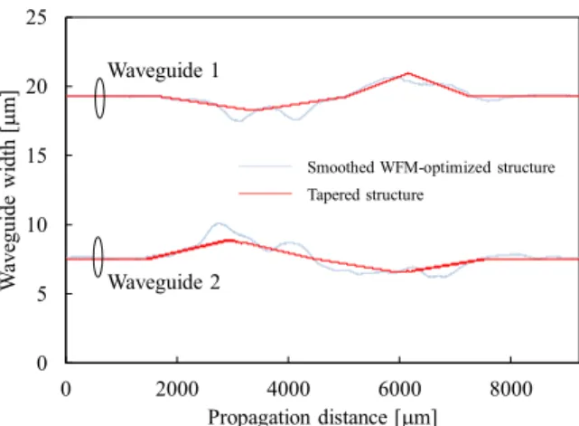
Here we discuss why the WFM-optimized structure has broadband characteristics. The smoothed waveguide widths of the WFM-optimized structure are shown in blue lines of Fig. 9. Since the optimized structure looks like a tapered structure, we suppose that tapered structure is one of the mechanisms of this broadband characteristics. It is reported that tapered structure expands bandwidth of directional couplers compared with conventional structure[20], [21].
Therefore, we try to approximate the optimized structure to tapered structure. The approximated tapered structure is shown in the red lines of Fig. 9. In order to determine the tapered structure, we introduced the phase rotation amount, given by following equation:
Δθ=
β(Wi,z)dz. (7)
Hereβ(Wi,z) is a propagation constant of each waveguidei (i=1, 2) at propagation distance ofz.β(Wi,z) is expressed as (2π/λ)neff(Wi,z), hereλis a wavelength 1.55 μm, and neff(Wi,z) is an effective index. The effective indices as a function of waveguide width at a wavelength of 1550 nm are shown in Fig. 10. Here, it is assumed thatΔ =0.386%, and h =6.0μm. Figure 11 (a) shows the effective indices vari- ation of each waveguide of the smoothed optimized struc- ture obtained by blue lines in Fig. 9, and Fig. 10. From Fig. 11 (a), we set the effective indices of tapered structure as shown in Fig. 11 (b), so thatΔθfor each waveguide through- out the structure is equal to that of optimized structure. Be- cause we determined the waveguide widths by increments of 0.1μm and the effective indices change with the waveguide
Fig. 9 Waveguide widths of smoothed WFM-optimized structure and ta- pered structure.
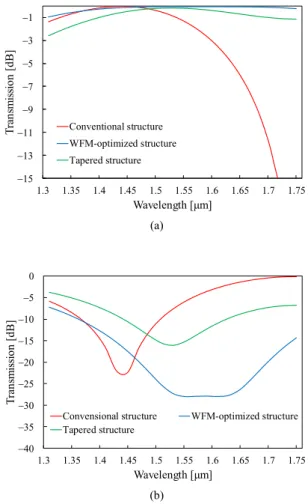
seen that, although the optimized structure has the most broadband characteristics, even the tapered structure has a wider bandwidth compared with conventional structure, suggesting tapered structure makes it broadband. However, in terms of crosstalk, while the optimized structure has the
Fig. 10 Waveguide width dependence of effective index.
Fig. 11 Effective indices variation of each waveguide of (a) the smoothed optimized structure and (b) tapered structure.
Fig. 12 Transmission spectra of (a) LP11amode at port 3 and (b) LP01
mode at port 4 of conventional directional coupler and the WFM-optimized structure and tapered structure.
lowest crosstalk, the improvement by tapered structure is little seen shown in Fig. 12 (b). Therefore, optimization by WFM method has advantage in crosstalk. We consider that the rapid oscillation, which cannot be represented in the ta- pered structure, contribute to the improvement of crosstalk.
Figures 13 (a) and (b) show the variations of effec- tive indices for waveguides of tapered and WFM-optimized structure at wavelength of 1350, 1550, and 1750 nm. The red lines show effective indices of Waveguide 2 and the blue lines show those of Waveguide 1. From Fig. 13, fol- lowing two mechanisms are speculated for the broadband characteristics. First, there are some points, at which phase- matching condition is satisfied for each wavelength due to the changes in waveguide widths. The second is compen- sation for coupling lengths. In general, the coupling length becomes longer with shorter wavelength due to strong con- finement. For 1350 nm, the difference in the effective index between two waveguides is small throughout the coupling region. On the other hand, for 1750 nm, the difference in the effective index between two waveguides is large for first half of the coupling region. LP01mode in Waveguide 2 and LP11a mode in Waveguide 1 in shorter wavelength, which need longer coupling length, are able to couple through the whole coupling region due to the small difference of ef-
Fig. 13 Effective indices variation of each waveguide in (a) the opti- mized structure and (b) tapered structure.
fective indices, while those in longer wavelength, which need shorter coupling length, are weakly coupled in the first part of the coupling region due to the larger difference of effective indices and coupled in the last half. The optimized structure compensates for the coupling length difference by changing the waveguide width.
5. Conclusion and Outlook
We reviewed a broadband PLC-based two-mode MUX/
DEMUX based on WFM-optimization. Theoretical results indicate that low-loss and broadband characteristics can be exploited by WFM-method. We suppose that the optimized structure has broadband characteristics mainly because of its tapered structure. Furthermore, the WFM-method less depends on parameters, it makes the design of PLC-device more freely. These results indicate that WFM-optimized mode MUX/DEMUX is a promising component for MDM transmission system.
Since the WFM method presented here is based on scalar BPM, it cannot be applied to the devices based on high-index-contrast waveguides, waveguides including po- larization conversion, and waveguide discontinuities. Cur- rently, we are developing WFM-method for these problems and can be found in[22]–[24].
50+25+10 km heterogeneous spans of few-mode fiber with inline erbium-doped fiber amplifier,” Optical Fiber Communication Con- ference, OTu2C.4, 2012.
[3] J.D. Love and N. Riesen, “Mode-selective couplers for few-mode optical fiber networks,” Opt. Lett., vol.37, no.19, pp.3990–3992, Oct. 2012.
[4] N. Hanzawa, K. Saitoh, T. Sakamoto, T. Matsui, S. Tomita, and M.
Koshiba, “Mode-division multiplexed transmission with fiber mode couplers,” Optical Fiber Communication Conference, OW1D.4, 2012.
[5] A. Li, J. Ye, X. Chen, and W. Shieh, “Low-loss fused mode coupler for few-mode transmission,” Optical Fiber Communication Confer- ence, OTu3G.4, 2013.
[6] S.G. Leon-Saval, N.K. Fontaine, J.R. Salazar-Gil, B. Ercan, R.
Ryf, and J. Bland-Hawthorn, “Mode-selective photonic lanterns for space-division multiplexing,” Opt. Express, vol.22, no.1, pp.1036–1044, Jan. 2014.
[7] N. Hanzawa, K. Saitoh, T. Sakamoto, T. Matsui, K. Tsujikawa, M. Koshiba, and F. Yamamoto, “Two-mode PLC-based mode multi/demultiplexer for mode and wavelength division multiplexed transmission,” Opt. Express, vol.21, no.22, pp.25752–25760, Nov.
2013.
[8] K. Saitoh, N. Hanzawa, T. Sakamoto, T. Fujisawa, Y. Yamashita, T. Matsui, K. Tsujikawa, and K. Nakajima, “PLC-based mode multi/demultiplexers for mode division multiplexing,” Optical Fiber Technology, vol.35, pp.80–92, Feb. 2017.
[9] T. Hashimoto, T. Saida, I. Ogawa, M. Kohtoku, T. Shibata, and H.
Takahashi, “Optical circuit design based on a wavefront-matching method,” Opt. Lett., vol.30, no.19, pp.2620–2622, Oct. 2005.
[10] Y. Sakamaki, T. Saida, T. Hashimoto, and H. Takahashi, “New op- tical waveguide design based on wavefront matching method,” J.
Lightw. Technol., vol.25, no.11, pp.3511–3518, Nov. 2007.
[11] Y. Sakamaki, T. Saida, T. Hashimoto, and H. Takahashi, “Low-loss Y-branch waveguides designed by wavefront matching method,” J.
Lightw. Technol., vol.27, no.9, pp.1128–1134, May 2009.
[12] Y. Sakamaki, T. Saida, T. Hashimoto, S. Kamei, and H. Takahashi,
“Loss reduction of waveguide crossings by wavefront matching method and their application to integrated optical circuits,” J.
Lightw. Technol., vol.27, no.13, pp.2257–2263, July 2009.
[13] T. Fujisawa, T. Kitoh, K. Watanabe, K. Suzuki, M. Kotoku, and H. Takahashi, “Wide-bandwidth, low-waveguide-width-sensi- tivity InP-based multimode interference coupler designed by wave- front matching method,” IEICE Electron. Express, vol.8, no.24, pp.2100–2105, Dec. 2011.
[14] Y. Yamashita, T. Fujisawa, S. Makino, N. Hanzawa, T. Sakamoto, T. Matsui, K. Tsujikawa, F. Yamamoto, K. Nakajima, and K. Saitoh,
“PLC-based LP11 mode rotator with curved trench structure deviced from wavefront matching method,” IEEE Photon. Technol. Lett., vol.29, no.13, pp.1063–1066, July 2017.
[15] Y. Yamashita, T. Fujisawa, S. Makino, N. Hanzasa, T. Sakamoto, T. Matsui, K. Tsujikawa, F. Yamamoto, K. Nakajima, and K.
Saitoh, “Design and fabrication of broadband PLC-based two-mode multi/demultiplexer using a wavefront matching method,” J. Lightw.
Technol., vol.35, no.11, pp.2252–2258, June 2017.
[16] B.R. West and S. Honkanen, “MMI devices with weak guiding de- signed in three dimensions using a genetic algorithm,” Opt. Express, vol.12, no.12, pp.2716–2722, June 2004.
[17] P.I. Borel, A. Harpøth, L.H. Frandsen, M. Kristensen, P. Shi,
guides,” J. Lightw. Technol., vol.20, no.10, pp.1876–1884, Oct.
2002.
[20] G.F.W. Michael and G.A. Teh, “Tapered optical directional coupler,”
Microw. Theory Techinique, vol.23, no.1, pp.85–92, Jan. 1975.
[21] N. Riesen and J.D. Love, “Ultra-broadband tapered mode-selective couplers for few-mode optical fiber networks,” IEEE Photon. Tech- nol. Lett., vol.25, no.24, pp.2501–2504, Dec. 2013.
[22] S. Makino, T. Fujisawa, and K. Saitoh, “Wavefront matching method based on full-vector finite-element beam propagation method for polarization control devices,” J. Lightw. Technol., vol.35, no.14, pp.2840–2845, July 2017.
[23] S. Makino, T. Fujisawa, and K. Saitoh, “Ultrasmall silicon mode converters designed by wavefront matching method developed for waveguide discontinuity problem,” IEEE Photonics Conference, TuG3.5, 2016.
[24] Y. Sawada, S. Makino, T. Fujisawa, and K. Saitoh, “Development of fully three-dimensional wavefront matching method and its applica- tion to the design of ultrasmall Si mode converters,” IEEE Photonics Conference, WG1.1, 2017.
Eri Taguchi received the B.S. degree in electronic engineering from Hokkaido Univer- sity, Sapporo, Japan, in 2016. She has been engaged in research on the modeling of pla- nar lightwave circuit using the finite element method. Ms. Taguchi is a student member of the Institute of Electronics, Information and Com- munication Engineers (IEICE) of Japan.
Takeshi Fujisawa was born in Sapporo, Japan, on January 12, 1979. He received the B.E., M.E., and Ph.D. degrees in electronic en- gineering from Hokkaido University, Sapporo, Japan, in 2001, 2003, and 2005, respectively. He was a Research Fellow of the Japan Society for the Promotion of Science from 2003 to 2006. In 2006, he joined the Nippon Telegraph and Tele- phone (NTT) Photonics Laboratories, NTT Cor- poration, Atsugi, Japan. In 2014, he became an Associate Professor in the Graduate School of Information Science and Technology, Hokkaido University. He is the Au- thor or Coauthor of more than 90 papers in international refereed journals.
His research interests include active optical devices for optical communica- tion systems, such as semiconductor lasers and modulators, and theoretical modeling of optical fibers and devices. He has been serving as an Asso- ciate Editor forOptics Expresssince 2014 and is a member of IEEE and the Institute of Electronics, Information and Communication Engineers of Japan.
Yoko Yamashita was born in Tokyo, Japan, on July 30, 1992. She received the B.S.
and M.S. degree in electronic engineering from Hokkaido University, Sapporo, Japan, in 2015 and 2017. She has been engaged in research on the modeling of planar lightwave circuit using the finite element method. Ms. Yamashita is a member of the Institute of Electronics, Informa- tion and Communication Engineers (IEICE) of Japan.
Shuntaro Makino was born in Hokkaido, Japan, on January 20, 1990. He received the B.S., M.S., and Ph.D. degrees in media and net- work technologies from Hokkaido University, Sapporo, Japan, in 2012, 2014, and 2016, re- spectively. He has been involved in research on the modeling of photonic integrated circuits us- ing the finite-element method.
Nobutomo Hanzawa received B.E., M.E.
degrees in electrical engineering and Dr. Eng.
degree from Yamagata University, Yonezawa, Japan, in 2005, 2007, and 2016 respectively.
Since 2007, he has been with NTT Access Net- work Service Systems Laboratories, NTT Cor- poration, Tsukuba, Japan. He has been engaged in research on optical fiber design, high-input- power characteristics in optical fiber, and few- mode transmission. Mr. Hanzawa is a member of the Institute of Electronics, Information and Communication Engineers (IEICE) of Japan.
Taiji Sakamoto received B.E., M.E. and Ph.D. degrees in electrical engineering from Osaka Prefecture University, Osaka, Japan, in 2004, 2006 and 2012, respectively. In 2006, he joined NTT Access Network Service Sys- tems Laboratories, NTT, Ibaraki, Japan, where he has been engaged in research on optical fiber nonlinear effects, low nonlinear optical fiber, few-mode fiber, and multi-core fiber for optical MIMO transmission systems. Dr. Sakamoto is a member of the Institute of Electronics, Informa- tion and Communication Engineers.
Takashi Matsui received B.E., M.E. and Ph. D. degrees in electronic engineering from Hokkaido University, Sapporo, Japan, in 2001, 2003 and 2008, respectively. He also attained the status of Professional Engineer (P.E.Jp) in electrical and electronic engineering in 2009. In 2003, He joined NTT Access Network Service Systems Laboratories, Ibaraki, Japan. He has been engaged in research on optical fiber design techniques. Dr. Matsui is a member of the Insti- tute of Electronics, Information and Communi- cation Engineers (IEICE) of Japan.
Kyozo Tsujikawa received the B.S. and M.S. degrees in chemistry, and the Dr. Eng.
degree from Tokyo Institute of Technology in 1990, 1992, and 2006, respectively. Since join- ing NTT, he has undertaken research on glasses for low-loss optical fibers and worked on the measurement of the optical fibers and worked on the measurement of the optical properties of fiber cables. He is now a Senior Research Engineer, NTT Access Network Service Sys- tems Laboratories, Tsukuba, Ibaraki, Japan. Dr.
Tsujikawa is a member of the Institute of Electronics, Information and Communication Engineers of Japan.
Kazuhide Nakajima (M’05) received M.S.
and Ph.D. degrees in electrical engineering from Nihon University, Chiba, Japan, in 1994 and 2005, respectively. In 1994, he joined NTT Access Network Systems Laboratories, Tokai, Ibaraki, Japan, where he engaged in research on optical fiber design and related measurement techniques. He is currently a Senior Research Engineer, Supervisor (Senior Distinguished Re- searcher) of NTT Access Network Service Sys- tems Laboratories, Tsukuba, Ibaraki, Japan. He is also acting as Rapporteur Q5/SG15 of ITU-T. Dr. Nakajima is a member of the Institute of Electronics, Information and Communication Engineers (IEICE), the Institute of Electrical and Electronics Engineers (IEEE) and the Optical Society (OSA).
Fumihiko Yamamoto received B.E., M.E.
and Dr. Eng. degrees from Kyushu University, Fukuoka, Japan, in 1989, 1991 and 2001, re- spectively. In 1991, he joined NTT Transmis- sion Systems Laboratories, Ibaraki, Japan. Dur- ing his 26-year career at NTT, he has been en- gaged in research and development related to optical access network design, and has planned and driven the strategy for introducing NTT’s research and development technologies. Since 2015 he has been managing the Research & De- velopment Planning Department in NTT Access Network Service Systems Laboratories as an executive research engineer. Dr. Yamamoto is a member of the Institute of Electronics, Information and Communication Engineers (IEICE) of Japan.
sociate Professor at Graduate School of Infor- mation Science and Technology, Hokkaido Uni- versity, and in 2013, he became a Professor there. He has been involved in research on fiber optics, nano-photonics, integrated optical devices, and computer-aided design and modeling of guided-wave devices. He is the author of more than 200 research papers in refereed international journals and more than 250 refereed international conference presentations. He is a member of the Institute of Electrical and Electronics Engineers (IEEE), the Optical Society of America (OSA), the Institute of Electronics, Information and Communication Engineers (IEICE). He was a Chair of Subcommittee D4 of Optical Fiber Communication Conference (OFC) in 2016. He is cur- rently a Technical Program Committee of European Conference on Optical Communication (ECOC). He received the Excellent Paper Award and the Young Scientist Award from the IEICE, in 1999 and 2002, respectively, the Young Scientists’ Prize of the Commendation for Science and Technology from the Ministry of Education, Culture, Sports, Science, and Technology (MEXT), Government of Japan in 2008, the JSPS Prize from the Japan So- ciety for the Promotion of Science in 2015, and the Distinguished Lecturers Award from the IEEE Photonics Society in 2017.