Switch Block Architecture for Multi-Context FPGAs
Using Hybrid Multiple-Valued/Binary Context Switching Signals
Yoshihiro NAKATANI, Masanori HARIYAMA and Michitaka KAMEYAMA
Graduate School of Information Sciences, Tohoku University
e-mail: {yoshi, hariyama, michi}@kameyama.ecei.tohoku.ac.jp
Abstract
Multi-context (MC) FPGAs have multiple memory bits per configuration bit forming configuration planes for fast switching between contexts. Large amount of memory causes significant overhead in area and power consumption. This paper presents two key technologies. The first is a floating-gate-MOS functional pass gate that merges storage and switching functions area-efficiently. The second is the use of a hybrid multiple-valued/binary context switching signal that eliminates redundancy of a conventional MC-switch with high scalability. The transistor count of the proposed MC-switch is reduced to 7% in comparison with that of a SRAM-based one.
1. Introduction
Dynamically-programmable gate arrays (DPGAs) provide more cost-effective implementations than conventional FPGAs where hardware resources are dedicated to a single context [1]. A DPGA can be sequentially configured as different processors in real time, and efficiently reuse the limited hardware resources in time. One of typical DPGA architectures is a multi-context one. Multi-context (MC) FPGAs have multiple memory bits per configuration bit forming configuration planes for fast switching between contexts. However, the additional memory planes cause significant overhead in area and power consumption [2]. Figure 1 shows the overall structure of an MC-FPGA. Each cell consists of a programmable Logic Block (LB) and a programmable Switch Block (SB). An MC-SB consists of multi-context switches (MC-switches). Each context is changed by the context switching signal (CS). The CS is broadcasted all the MC-switches. Figure 2 shows the structure of a conventional SRAM (Static Random Access Memory) -based MC-switch for 4 contexts. Each MC-switch selects a configuration bit between pre-stored configuration bits according to CS. The pass transistor is ON for G=1, and OFF for G=0. A conventional SRAM-based MC-switch requires N SRAM bits for N contexts.
CS: Context Switching Signal C: Cell
S: Multi-Context Switch
Fig. 1 Overall structure of an MC-FPGA.
M: SRAM (Static Random Access Memory) bit G: Configuration bit
Fig. 2 Equivalent circuit of conventional MC-switch (4 contexts).
To overcome the overhead, it has proposed many ways before now. One of the ways is the way which is applied that configuration data rarely changes [3]. And another one is the way that uses floating-gate MOS functional pass-gate (FGFP) using floating-gate MOS transistor (FGMOS) with multiple-valued signal for switching between contexts [4],[5]. The work [4] proposed an MC-switch with 4 FGMOSs that use a multiple-valued signal for context switching.
In order to reduce the overhead of configuration memory in MC-FPGAs, we employ a FGFP that merges storage and switching function on a single FGMOS. In this MC-switch, several pass transistors become ON
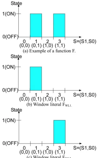
(a) Example of a function F.
(b) Window literal FWL1.
(c) Window literal FWL2. Fig. 3 Function of an MC-switch (4 contexts).
redundantly for some configuration patterns. To eliminate this redundancy, a hybrid multiple-valued/ binary context switching signal is used for context switching. The proposed MC-switch has only 2 FGMOSs, each of which is exclusively ON. Although the proposed MC-switch requires more complex circuit for generating the context switching signal, they can shared among several MC-switches, and its overhead is negligible.
In the case of more 4 contexts, although the transistor count of an MC-switch that proposed in [5] increases nonlinearity, that of an MC-switch that proposed in this paper increase linearity. Using the proposed MC-switch, the transistor count is reduced significantly as increasing contexts.
The transistor count of MC-switch is reduced to 7% and 50% in comparison with that of the SRAM-based MC-switch and the MC-switch using only multiple-valued FGFPs, respectively. The transistor count of the proposed MC-SB is reduced to 8% and 60% in comparison with that of the SRAM-based MC-SB and the MC-SB using only multiple-valued FGFPs, respectively.
(a) An up-literal.
(b) A down literal.
Fig. 4 An up-literal and a down-literal (4 contexts).
Fig. 5 MC-switch using 4 FGFPs (4 context).
2. Architecture of Multi-Context Switch
This section describes the MC-switch using only a multiple-valued context switching signal.
Figure 3(a) shows an example of the function F of an MC-switch that is ON only for CS = 1 and 3. The function F can be given by “OR-ing” the function FWL1
(Fig.3(b)) and FWL2 (Fig.3(c)), each of which is called a
window literal. Given S1 and S2 (S1
≤
S2), a window literal is defined as follows: ≤ ≤ = otherwise S S S S S S FWL 2 1 0 1 ) 2 , 1 , ( .
The function F is given by “OR-ing” two window literals as follows: ) 3 , 2 , ( ) 1 , 0 , ( ) (S F S S S F S S S F = WL + WL .
The window literal can be AND-ing the functions FUL
and FDL called “up-literal” and “down-literal”,
respectively. An up-literal is a monotone increasing function as shown in Fig. 4(a). Given the threshold value T, an up-literal FUL(S,T) is given by
≤ = otherwise S T T S FUL 0 1 ) , ( .
Fig. 6 The circuit of an MC-switch (8 contexts).
A down-literal is monotone decreasing function as shown in Fig. 4(b). Given the threshold value T, a down-literal FDL(S,T) is given by
≤
=
otherwise
T
S
T
S
F
L0
1
)
,
(
D .A window literal FWL is given by “AND-ing” the
function FUL and FDL as follows:
)
2
,
(
)
1
,
(
)
2
,
1
,
(
S
S
S
F
S
S
F
S
S
F
WL=
UL•
DL .Each of an up-literal and a down–literal can be implemented only a single FGFP [3]. Therefore a window literal is implemented by series-connected FGMOSs for wired-AND. An MC-switch is implemented by connecting the circuit for window literal parallel for wired-OR as shown in Fig.5. Four FGMOSs are sufficient for 4 contexts since the function of an MC-switch includes 2 window literals at most. Let us consider implementing more than 4 contexts. Figure 6 shows the MC-switch for 8 contexts. It consists of 2 MC-switches for 4 contexts and an additional multiplexer (MUX).
In the case of 4 contexts, the window-literal based implementation of the MC-switch has redundancy. For example, it requires 4 FGMOSs even when the function of the MC-switch is a single window literal.
3. Architecture of an MC-Switch Using
Hybrid Multiple-Valued/Binary Context
Switching Signals
Figure 7 shows an example of a hybrid multiple- valued/binary context switching signal. Figure 8 shows the circuit to generate the hybrid multiple- valued/binary context switching signal. The circuit of generating the hybrid multiple- valued/binary context switching signal is small and that is broadcasted all MC-
(a) The waveform of S0 and Vs.
(b) The waveform of S0 and  ̄Vs.
(c) The waveform of  ̄S0 and Vs.
(d) The waveform of  ̄S0 and  ̄Vs.
Fig. 7 Waveforms of hybrid multiple-valued/binary context switching signals.
switches. The overhead of using the hybrid multiple-valued/binary context switching signal is small. The output is same as the multiple-valued CS signal when the binary CS signal is 1. Otherwise, the output is 0. Hybrid multiple-valued/binary signals are defined as follows:
=
=
=
)
0
0
(
)
1
0
(
0
0
S
S
Vs
Vs
and
S
,
=
=
=
)
0
0
(
)
1
0
(
0
0
S
S
Vs
Vs
and
S
,
(a) The symbol of the circuit performs the hybrid multiple-valued/binary context switching signal.
(b) The circuit performs the hybrid multiple-valued/ binary context switching signal.
Fig. 8 The circuit which makes a hybrid multiple-valued/binary context switching signal.
=
=
=
)
0
0
(
)
1
0
(
0
0
S
S
Vs
Vs
and
S
,
=
=
=
)
0
0
(
)
1
0
(
0
0
S
S
Vs
Vs
and
S
.
The context ID CS = {0,1,2,3} is represented by a voltage Vs = {1,2,3,4}. The reason why CS = 0 corresponds to Vs = 1 is that (S0 and Vs) and ( ̄S0 and
Vs) make difference when CS = 0. The multiple-valued signals, Vs and  ̄Vs are defined as follows:
1
0
1
*
2
+
+
=
S
S
Vs
,Vs
Vs
= 5
−
.It is necessary to make a clear distinction between the 0-level of binary and that of multiple-valued. It is necessary that multiple-valued signal has 5-level.
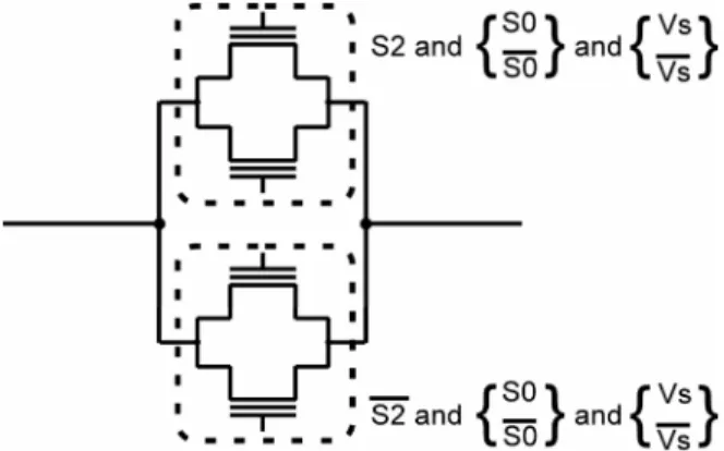
Figure 9 shows the circuit of an MC-switch using a hybrid multiple-valued/binary context switching signal. The FGMOS Tr1 works when S0 = 1 (Vs = 2, 4), and the gate input of Tr1 is selected from two signals: “S0 and Vs” and “S0 and  ̄Vs”. Similarly, the FGMOS Tr2
works when S0 = 0 (Vs = 1, 3), and the gate input of Tr2 is selected from two signals: “ ̄S0 and Vs” and “ ̄S0
and  ̄Vs”.
Fig. 9 A circuit of an MC-switch using hybrid multiple-valued/binary context switching signals.
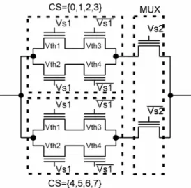
Fig. 10 The circuit of an MC-switch using hybrid multiple-valued/binary context switching signals (8 contexts).
Threshold operation for “AND-ing” the multiple- valued context switching signal and the binary one implements the same function as “AND-ing” two window literals. If we do not consider transistors to select the control signals, only 2 FGMOSs are sufficient for an MC-switch for 4 contexts. Table 1 shows the relations between configuration data, the context switching signals, and threshold voltages of Tr1 and Tr2. From Table 1, all of context patterns for 4 contexts can be generated only by 2 FGMOSs.
Let us consider implementing more than 4 contexts. Figure 10 shows the MC-switch for 8 contexts using hybrid multiple-valued/binary context switching signals. It consists of 2 MC-switches for 4 contexts. Note that it does not require any additional MUX unlike the MC-switch using only the multiple-valued context switching signal. That is because more context selection bits such as S2 are merged into the hybrid multiple- valued/binary context switching signal without any overhead.
Table 1 The selection of Vth and control lines in MC-switches.
Fig. 11 The circuit of an MC-SB (4 contexts).
Let us consider a Multi-context Switch Block (MC-SB). Figure 11 shows the circuit of an MC-SB. The MC-SB has the structure of cross bar network. The MC-switches is used as a cross-point switch. For simplicity, three the MC-SB has 3 columns and 3 rows. For a certain context, a single cross point switch on each column and row is ON at most. We can map the possibly-ON cross-point
switch on a column to the same MC-switch on the column for any context. As a result, N independent control signals are sufficient for an N・N MC-SB. In other words, a context switching signal is shared with MC-switches on the same column.
4. Evaluation
We simulated the function of an MC-switch using the hybrid multiple-valued/binary context switching signal. Figure 12(a) shows the simulated circuit. We used the simulator “HSPICE” for simulation. In the simulation, we replace FGMOSs with MOS transistors. Programming the threshold voltage of an FGMOS is implemented by changing HSPICE parameter. Set the configuration data CS{0,1,2,3} = {0,1,0,1}. The result is shown in Fig. 12(b). Only when CS is 1 or 3, the input is transferred to the output.
We compare the transistor count of the proposed MC-switch and the proposed MC-SB with the SRAM-based MC-switch and MC-SB respectively for 4 contexts. The transistor count of the proposed MC-switch is reduced to 7% of SRAM-based one (Table 2). Table 3 show the comparison result when assuming that the switch block consists of 10×10 cross-point switches. The transistor count of the proposed MC-SB is reduced to 8% of that of the SRAM-based one. Figure 13 shows the proposed MC-switch has more advantage than SRAM-based one as the size of MC-SB increases.
configuration data Tr1 Tr2
context0 context1 context2 context3 Vth Control line Vth Control line
0 0 0 0 5 S0 and Vs 5  ̄S0 and Vs 0 0 0 1 1.5 S0 and Vs 5  ̄S0 and Vs 0 0 1 0 5 S0 and Vs 1.5  ̄S0 and Vs 0 0 1 1 1.5 S0 and Vs 1.5  ̄S0 and Vs 0 1 0 0 1.5 S0 and  ̄Vs 5  ̄S0 and Vs 0 1 0 1 0.5 S0 and Vs 5  ̄S0 and Vs 0 1 1 0 1.5 S0and  ̄Vs 1.5  ̄S0 and Vs 0 1 1 1 0.5 S0 and Vs 1.5  ̄S0 and Vs 1 0 0 0 5 S0 and Vs 1.5  ̄S0 and  ̄Vs 1 0 0 1 1.5 S0 and Vs 1.5  ̄S0 and  ̄Vs 1 0 1 0 5 S0 and Vs 0.5  ̄S0 and Vs 1 0 1 1 1.5 S0 and Vs 0.5  ̄S0 and Vs 1 1 0 0 1.5 S0and  ̄Vs 1.5  ̄S0 and  ̄Vs 1 1 0 1 0.5 S0 and Vs 1.5  ̄S0 and  ̄Vs 1 1 1 0 1.5 S0and  ̄Vs 0.5  ̄S0 and Vs 1 1 1 1 0.5 S0 and Vs 0.5  ̄S0 and Vs
(a) The circuit of simulation about an MC-switch using hybrid multiple-valued/binary context switching
signals.
(b) The result of simulation about an MC-switch using multiple-valued/binary context switching signals.
Fig. 12 The simulated circuit and the result.
0 50000 100000 150000 200000 250000 300000 350000 0 20 40 60 80 100
The number of columns of a switch block
Th e n u m ber of tr ansi st or s SRAM-based one Only multiple-valued-based one Proposed one
Fig. 13 The relationship between the number of columns of an MC-SB and the number of transistors.
5. Conclusion
This paper presents MC-switch architecture. The key technologies are a FGFP and the use of a hybrid multiple-valued/binary context switching signal. Using FGFPs for MC-switch, the area of an MC-switch is less
Table 2 The transistor count of an MC-switch.
Transistor count
SRAM-based one 31
Only multiple-valued-
FGFP-based one [4] 4
Proposed one 2
Table 3 The transistor count of an MC-SB (10×10).
Transistor count
SRAM-based 3100 Only multiple-valued-
FGFP-based one [4] 400
Proposed one 240
than that of the SRAM-based one. Using the hybrid multiple-valued/binary context switching signal, the area of an MC-switch becomes small further. The use of FGFPs will be efficient in static power consumption in comparison with the SRAM-based one because no supply voltage is required to keep the storage.
Acknowledgment
This work was supported by Industrial Technology Research Grant Program from New Energy and Industrial Technology Development Organization (NEDO) of Japan.
This work is supported by VLSI Design and Education Center (VDEC), the University of Tokyo in collaboration with Synopsys, Inc.
References
[1] A.DeHon. Dynamically programmable gate arrays: a step toward increased computational density. In
the Fourth Canadian Workshop on Field-Programmable Devices, pages 47-54, (1996)
[2] S. Trimberger, D. Carberry, A. Johnson and J. Wong, “A Time-multiplexed FPGA,” Proc. of
FCCM’97, pp.22-28 (1997)
[3] W. Chong, M. Hariyama, M. Kameyama, “Novel switch-block architecture using reconfigurable context memory for multi-context FPGAs,”
International Workshop on Applied Reconfigurable Computing, (2005)
[4] T. Hanyu, M. Kameyama, “Multiple-Valued Logic-in-Memory VLSI Architecture Based on Floating-Gate-MOS Pass-Transistor Logic,” IEICE
Trans. Electron., Vol.E82-C, No.9 (1999)
[5] M. Hariyama, W. Chong, S. Ogata, M. Kameyama, “Novel Switch Block Architecture Using Non-Volatile Functional Pass-gate for Multi-Context FPGAs,” IEEE Computer Society