Si5332 データ・シート
6/8/12 の出力・任意周波数のクロック・ジェネレータ
Silicon Labs 独自の柔軟な周波数合成テクノロジー、MultiSynth™ に基づいた Si5332 は、
優れたジッタ性能 (190 fs rms) を実現しながら、任意の組み合わせの出力周波数を生成 します。デバイスの極めて柔軟なアーキテクチャにより、0 ppm の周波数合成エラーを 実現しながら、1 つのデバイスで最大 12 個の差動クロック出力の幅広い整数および非整 数関係周波数を生成することができます。デバイスは、独立した電圧にそれぞれ接続で きる複数の出力バンクを提供するため、供給電圧が混在するアプリケーションに使用で きます。さらに、各クロック出力の信号フォーマットはユーザによる構成が可能です。 周波数、フォーマット、供給電圧の柔軟性を備えた Si5332 を使用することで、複数のク ロック IC と発振器を 1 つのデバイスに置き換えることができます。
Si5332 は、ClockBuilder Pro™ ソフトウェアを使用して素早く簡単に構成できます。
ClockBuilder Pro は、固有の構成ごとにカスタム部品番号を割り当てます。カスタム部 品番号を使って注文されたデバイスは、出荷時に無料で工場でプログラムされるため、 各アプリケーションに応じてクロックを簡単にカスタマイズできます。Si5332 は、I2C シリアル・インターフェイスを使用してプログラムすることもできます。 アプリケーション: • サーバ、ストレージ、検索の高速化 • イーサネット・スイッチ、ルータ • スモール・セル、モバイル・バックホー ル/フロントホール • 画像印刷 • 通信 • 放送用ビデオ • テストおよび測定 • 産業用、組み込みコンピューティング 主な機能 • 任意周波数 6/8/12 出力、プログラム可能な クロック・ジェネレータ • 出力クロックとユーザ構成可能なハードウ ェア入力ピンの異なる組み合わせをサポー トする 3 種類のパッケージ・サイズ • 32 ピン QFN、最大 6 つの出力 • 40 ピン QFN、最大 8 つの出力 • 48 ピン QFN、最大 12 個の出力 •MultiSynth テクノロジーにより、最大 250 MHz までの出力の任意の周波数合成が可 能 • 高度な構成が可能な出力パス、クロスポイ ント・マルチプレクサを搭載 • 最大 3 つの独立した非整数合成出力パ ス • 最大 5 つの独立した整数分周器 • 組み込み 50 MHz 水晶オプション • 入力周波数帯域: • 外部水晶:16 ~ 50 MHz • 差動クロック:10 ~ 250 MHz • LVCMOS クロック:10 ~ 170 MHz • 出力周波数帯域: • 差動:5 ~ 333.33 MHz • LVCMOS:5 ~ 170 MHz • 出力毎のユーザ構成可能なクロック出力信 号フォーマット:LVDS、LVPECL、HCSL、 LVCMOS • マルチ・プロファイル構成をサポート • 温度範囲:-40 ~ +85 °C • ダウンおよびセンター・スプレッド・スペ クトラム •RoHS-6 準拠 •Si5332 ファミリ・リファレンス・マニュア ル
Table of Contents
1. Features List . . . 4
2. Ordering Guide
. . . 5
3. Functional Description. . . 6
3.1 Functional Block Diagrams . . . 7
3.2 Modes of Operation . . . 9
3.2.1 Initialization . . . 9
3.3 Frequency Configuration . . . 9
3.4 Inputs . . . .10
3.4.1 External Reference Input (XA/XB) . . . .10
3.4.2 Input Clocks . . . .10
3.4.3 Input Selection . . . .10
3.5 Outputs . . . .11
3.5.1 Output Signal Format . . . .11
3.5.2 Differential Output Terminations. . . .12
3.5.3 LVCMOS Output Terminations . . . .16
3.5.4 LVCMOS Output Signal Swing . . . .16
3.5.5 LVCMOS Output Polarity . . . .16
3.5.6 Output Enable/Disable . . . .16
3.5.7 Differential Output Configurable Skew Settings. . . .16
3.5.8 Synchronous Output Disable Feature . . . .16
3.6 Spread Spectrum. . . .17
3.7 Universal Hardware Input Pins . . . .17
3.8 Custom Factory Pre-programmed Parts . . . .18
3.9 I2C Serial Interface . . . .18
3.10 In-Circuit Programming . . . .19
4. Register Map
. . . 20
5. Electrical Specifications
. . . 21
6. Pin Descriptions
. . . 36
6.1 Pin Descriptions (48-QFN) . . . .36
6.2 Pin Descriptions (40-QFN) . . . .41
6.3 Pin Descriptions (32-QFN) . . . .46
7. Package Outline
. . . 50
7.6 Si5332 5x5 mm 32-QFN Package Diagram, Embedded Crystal Versions (Si5332E/F/G/H) . . . .56
8. PCB Land Pattern
. . . .57
8.1 Si5332A/B/C/D 48-QFN Land Pattern . . . .57
8.2 Si5332A/B/C/D 40-QFN Land Pattern . . . .59
8.3 Si5332A/B/C/D 32-QFN Land Pattern . . . .61
8.4 Si5332E/F/G/H 48-LGA Land Pattern . . . .63
8.5 Si5332E/F/G/H 40-LGA Land Pattern . . . .65
8.6 Si5332E/F/G/H 32-LGA Land Pattern . . . .67
9. Top Marking . . . .
69
第
1 章 機能リスト
• 任意周波数 6/8/12 出力、プログラム可能なクロック・ジェネレ ータ • 出力クロックとユーザ構成可能なハードウェア入力ピンの異な る組み合わせをサポートする 3 種類のパッケージ・サイズ • 32 ピン QFN、最大 6 つの出力 • 40 ピン QFN、最大 8 つの出力 • 48 ピン QFN、最大 12 個の出力 • MultiSynth™ テクノロジーにより、最大 250 MHz までの出力の 任意の周波数合成が可能 • 最大 333.33 MHz の整数出力周波数 • 組み込み 50 MHz 水晶オプション • 高度な構成が可能な出力パス、クロスポイント・マルチプレク サを搭載 • 最大 3 つの独立した非整数合成出力パス • 最大 5 つの独立した整数分周器 • 組み込み 50 MHz 基準水晶の注文オプション • 入力周波数帯域: • 外部水晶:16 ~ 50 MHz • 差動クロック:10 ~ 250 MHz • LVCMOS クロック:10 ~ 170 MHz • 出力周波数帯域: • 差動:5 ~ 333.33 MHz • LVCMOS:5 ~ 170 MHz • 組み込み基準水晶オプション (E/F/G/H グレード) • 出力毎のユーザ構成可能なクロック出力信号フォーマット: LVDS、LVPECL、HCSL、LVCMOS • 低位相ジッタ: • 175 fs RMS (組み込み水晶) • 190 fs RMS (外部水晶) • PCIe Gen1/2/3/4、SRIS 準拠 • 1.8 V、2.5 V、3.3 V コア VDD • 調整可能な出力間遅延 • マルチ・プロファイル構成をサポート: • 同じカスタム部品番号で最大 16 の入力/出力構成を保存 • グリッチのない独立したオンザフライ出力周波数変更 • 非常に低い消費電力 • 各出力バンクの独立した出力電源ピン: • 1.8 V、2.5 V、または 3.3 V 差動 • 1.5 V、1.8 V、2.5 V、3.3 V LVCMOS • プログラム可能なスプレッド・スペクトラム • ダウンおよびセンター・スプレッド(30 ~ 33 kHz で –0.1% –2.5%、0.01% ステップ) • 電源フィルタリング内蔵 • シリアル・インターフェイス:I2C • ClockBuilder Pro ソフトウェア・ユーティリティにより、デバ イスの構成とカスタム部品番号の割り合てを簡素化 • 動作温度範囲:-40 ~ +85 °C • RoHS-6 準拠機能リスト
2. Ordering Guide
Si5332X DXXXXX - GMpR
D = Product Revision
XXXXX = NVM code. Aa unique 5-digit ordering sequence will be assigned by ClockBuilder Pro
Operating Temp Range: -40 to +85 C GM = QFN, ROHS6 compliant P = 1 for 6-output, 32-pin QFN
2 for 8-output, 40-pin QFN 3 for 12-output, 48-pin QFN R = Tape & Reel (ordering option)
Ordering Part Number
Input Type Output Clock Frequency Range Operating Temperature Range Si5332A 5MHz - 333.33MHz Si5332B 5MHz - 200MHz Si5332C 5MHz - 333.33MHz Si5332D 5MHz - 200MHz Si5332E 5MHz - 333.33MHz Si5332F 5MHz - 200MHz Si5332G 5MHz - 333.33MHz Si5332H 5MHz - 200MHz
Frequency Synthesis Mode
Integer and Fractional mode External crystal or Clock Integer and Fractional mode
Integer mode only
Integer mode only -40 to +85C
Integer and Fractional mode Embedded crystal or External Clock Integer and Fractional mode
Integer mode only Integer mode only
D = Product Revision
Operating Temp Range: -40 to +85 C GM = QFN, ROHS6 compliant p = 1 for 6-output, 32-pin QFN
2 for 8-output, 40-pin QFN 3 for 12-output, 48-pin QFN R = Tape & Reel (ordering option)
Ordering Part Number
Input Type Output Clock Frequency Range Operating Temperature Range Si5332A 5MHz - 333.33MHz Si5332B 5MHz - 200MHz Si5332C 5MHz - 333.33MHz Si5332D 5MHz - 200MHz Si5332E 5MHz - 333.33MHz Si5332F 5MHz - 200MHz Si5332G 5MHz - 333.33MHz Si5332H 5MHz - 200MHz
Frequency Synthesis Mode
Integer and Fractional mode External crystal or Clock Integer and Fractional mode
Integer mode only
Integer mode only -40 to +85C
Integer and Fractional mode Embedded crystal or External Clock Integer and Fractional mode
Integer mode only Integer mode only
Pre-programmed devices using a ClockBuilder Pro configuration file
Si5332X - D - GMpR
Blank devices, in-system programmable
Figure 2.1. Orderable Part Number Guide
3. Functional Description
The Si5332 is a high-performance, low-jitter clock generator capable of synthesizing up to twelve user-programmable clock frequencies up to 333.33 MHz. The device supports free run operation using an external or embedded crystal, or it can lock to an external clock signal. The output drivers support up to twelve differential clocks or twenty four LVCMOS clocks, or a combination of both. The output drivers are configurable to support common signal formats, such as LVPECL, LVDS, HCSL, and LVCMOS. VDDO pins are provided for versatility, which can be set to 3.3 V, 2.5 V, 1.8 V or 1.5 V (CMOS only) to power the multi-format output drivers. The core voltage supply (VDD) accepts 3.3 V, 2.5 V, or 1.8 V and is independent from the output supplies (VDDOxs). Using its two-stage synthesis archi-tecture and patented high-resolution low-jitter MultiSynth technology, the Si5332 can generate an entire clock tree from a single device. The Si5332 combines a wideband PLL with next generation MultiSynth technology to offer the industry’s highest output count high per-formance programmable clock generator, while maintaining a jitter perper-formance below 200 fs RMS. The PLL locks to either an external 16-50 MHz crystal or an embedded 50 MHz crystal for generating free-running clocks or to an external clock (CLKIN_2/CLKIN_2# or CLKIN_3/CLKIN_3#) for generating synchronous clocks. In free-run mode, the oscillator frequency is multiplied by the PLL and then divided down either by an integer divider or MultiSynth for fractional synthesis.
The Si5332 features user-defined universal hardware input pins which can be configured in the ClockBuilder Pro software utility. Uni-versal hardware pins can be used for OE, spread spectrum enable, input clock selection, output frequency selection, or I2C address select.
The device provides the option of storing a user-defined clock configuration in its non-volatile memory (NVM), which becomes the de-fault clock configuration at power-up. To enable in-system programming, a power up mode is available through OTP which powers up the chip in an OTP defined default mode but with no outputs enabled. This allows a host processor to first write a user defined subset of the registers and then restart the power-up sequence to activate the newly programmed configuration without re-downloading the OTP.
3.1 Functional Block Diagrams
Si5332-GM3: 12-Output, 48-QFN
Multi Synth Multi Synth INT INT INT INT NVM I2C SCLK SDATA HW Input Control Input1 Input2 Input3 Input4 Input5 Input6 Input7 VDDO4 OUT9 OUT9b ÷INT OUT10 VDDO5 OUT10b ÷INT OUT11 OUT11b ÷INT Bank D OUT0 VDDO0 OUT0b ÷INT VDDO2 OUT3 OUT3b ÷INT OUT4 OUT4b ÷INT OUT5 OUT5b ÷INT Bank B OUT1 VDDO1 OUT1b ÷INT OUT2 OUT2b ÷INT Bank A VDDO3 OUT6 OUT6b ÷INT OUT7 OUT7b ÷INT OUT8 OUT8b ÷INT Bank C XTAL OSCSi5332A/B/C/D: External Crystal Si5332E/F/G/H: Internal Crystal
PLL ÷INT CLKIN_3 CLKIN_3b CLKIN_2 CLKIN_2b INT
Figure 3.1. Block Diagram for 12-Output Si5332 in 48-QFN The Si5332-GM3 48-QFN features:
• Up to twelve differential clock outputs, with six VDDO pins.
• Seven user-configurable HW input pins, defined using ClockBuilder Pro.
Si5332-GM2: 8-Output, 40-QFN
Multi Synth INT Multi Synth INT INT INT INT OUT0 VDDO0 VDDO3 OUT4 OUT1 VDDO1 OUT2 VDDO2 OUT0b OUT4b OUT1b OUT2b ÷INT ÷INT ÷INT ÷INT NVM I2C SCLK SDATA PLL VDDO4 OUT6 OUT6b ÷INT VDDO5 OUT7 OUT7b ÷INT OUT3 OUT3b ÷INT OUT5 OUT5b ÷INT HW Input Control Input1 Input2 Input3 Input4 Input5 Input6 Input7 Bank A Bank B CLKIN_3 CLKIN_3b CLKIN_2 XTAL OSC CLKIN_2bSi5332A/B/C/D: External Crystal Si5332E/F/G/H: Internal Crystal
÷INT
Figure 3.2. Block Diagram for 8-Output Si5332 in 40-QFN The Si5332-GM2 40-QFN features:
• Up to eight differential clock outputs, with six VDDO pins.
• Seven user-configurable HW input pins, defined using ClockBuilder Pro.
Si5332-GM1: 6-Output, 32-QFN
Multi Synth INT Multi Synth INT INT INT INT OUT0 VDDO0 VDDO3 VDDO4 VDDO5 OUT3 OUT4 OUT5b OUT1 VDDO1 OUT2 VDDO2 OUT0b OUT3b OUT4b OUT5 OUT1b OUT2b ÷INT ÷INT ÷INT ÷INT ÷INT ÷INT NVM I2C HW Input Control SCLK SDATA Input1 Input2 Input3 Input4 Input5 PLL CLKIN_2 XTAL OSC CLKIN_2bSi5332A/B/C/D: External Crystal Si5332E/F/G/H: Internal Crystal
÷INT
Figure 3.3. Block Diagram for 6-Output Si5332 in 32-QFN The Si5332-GM1 32-QFN features:
• Up to six differential clock outputs with individual VDDO.
• Five user-configurable HW input pins, defined using ClockBuilder Pro. 3.2 Modes of Operation
The Si5332 supports both free-run and synchronous modes of operation. The default mode selection is set in ClockBuilder Pro. Alterna-tively, two universal hardware input pins can be defined as CLKIN_SEL[1:0] to select between a crystal or clock input. There is also the option to select the input source via the serial interface by writing to the input select register.
3.2.1 Initialization
Once power is applied, the device begins an initialization period where it downloads default register values and configuration data from NVM and performs other initialization tasks. Communicating with the device through the serial interface is possible once this initializa-tion period is complete. The clock outputs will be squelched until the device initializainitializa-tion is done.
3.3 Frequency Configuration
The phase-locked loop is fully integrated and does not require external loop filter components. Its function is to phase lock to the selec-ted input and provide a common synchronous reference to the high-performance MultiSynth fractional or integer dividers.
A cross point mux connects any of the MultiSynth divided frequencies or INT divided frequencies to individual output drivers or banks of output drivers. Additional output integer dividers provide further frequency division by an even integer from 1 to 63. The frequency con-figuration of the device is programmed by setting the input dividers (P), the PLL feedback fractional divider (Mn/Md), the MultiSynth fractional dividers (Nn/Nd), and the output integer dividers (R). Silicon Labs’ Clockbuilder Pro configuration utility determines the opti-mum divider values for any desired input and output frequency plan
3.4 Inputs
The Si5332 requires an external 30–50 MHz crystal at its XIN/XOUT pins or the embedded 50 MHz crystal to operate in free-run mode, or an external input clock (CLKIN_2/CLKIN_2# or CLKIN_3/CLKIN_3#) for synchronous operation. An external crystal is not required in synchronous mode.
3.4.1 External Reference Input (XA/XB)
An external crystal (XTAL) is used in combination with the internal oscillator (OSC) on Si5332A/B/C/D to produce a low jitter reference for the PLL when operating in the free-run mode. The Si5332 Reference Manual provides additional information on PCB layout recom-mendations for the crystal to ensure optimum jitter performance. Refer to Table 5.4 External Crystal Input Specification on page 24 for crystal specifications.
For free-running operation, the internal oscillator can operate from a low-frequency fundamental mode crystal (XTAL) with a resonant frequency of 16 to 50 MHz. A crystal can easily be connected to pins XA and XB without external components, as shown in the figure below. Internal loading capacitance (CL) values from 2 pf to 30 pf can be selected via register settings or internal CL can be totally disabled allowing for external CL. Alternatively, an external CL can be used along with the internal CL.
Osc
To synthesis stage
or output selectors
XTAL
XA
XB
Figure 3.4. External Reference Input (XA/XB)
The Si5332E/F/G/H options feature an embedded 50 MHz reference crystal that is used in the free run mode. 3.4.2 Input Clocks
An input clock is available to synchronize the PLL when operating in synchronous mode. This input can be configured as LVPECL, LVDS or HCSL differential, or LVCMOS. The recommended input termination schemes are shown in the Si5332 Family Reference Manual. Differential signals must be AC coupled. Unused inputs can be disabled by register configuration.
3.4.3 Input Selection
The active clock input is selected by register control, or by defining two universal input pins as CLKIN_SEL[1:0] in ClockBuilder Pro. A register bit determines input selection as pin or register selectable. If there is no clock signal on the selected input at power up, the device will not generate output clocks.
In a typical application, the Si5332 reference input is configured immediately after power-up and initialization. If the device is switched to another input more than ±1000 ppm offset from the initial input, the device must be recalibrated manually to the new frequency, tem-porarily turning off the clock outputs. After the VCO is recalibrated, the device will resume producing clock outputs. If the selected inputs are within ±1000 ppm, any phase error difference will propagate through the device at a rate determined by the PLL bandwidth. Hitless switching and phase build-out are not supported by the Si5332.
3.5 Outputs
The Si5332 supports up to 12 differential output drivers. Each output can be independently configured as a differential pair or as dual LVCMOS outputs. The 8-output and 12-output devices feature banks of outputs, with each bank sharing a common VDDO.
Table 3.1. Clock Outputs
Device/Package Maximum Outputs
Si5332-GM1 (32-QFN) 6 Differential, 12 LVCMOS
Si5332-GM2 (40-QFN) 8 Differential, 16 LVCMOS
Si5332-GM3 (48-QFN) 12 Differential, 24 LVCMOS
The output stage is different for each of the three versions of Si5332.
• The 6-output device features individual VDDO pins for each clock output. Each clock output can be sourced from MultiSynth0, Multi-Synth1, the input reference clock, or one of the five INT dividers through the cross point MUX.
• The 8-output device includes four clock outputs with dedicated VDDO pins, each of which can be sourced from MultiSynth0, Multi-Synth1, the input reference clock, or one of the five INT dividers through the cross point MUX. The remaining four clock outputs are divided into Bank A and Bank B. Each Bank of outputs can be sourced from MultiSynth0, MultiSynth1, the input reference clock, or one of the five INT dividers through the cross point MUX. The outputs within each of the two Banks share a common VDDO pin. • The 12-output device includes two clock outputs with dedicated VDDO pins, each of which can be sourced from MultiSynth0,
Multi-Synth1, the input reference clock, or one of the five INT dividers through the cross point MUX. The remaining ten clock outputs are divided into Bank A, Bank B, Bank C, and Bank D. Each Bank of outputs can be sourced from MultiSynth0, MultiSynth1, the input reference clock, or one of the five INT dividers through the cross point MUX. The outputs within each of the four Banks share a common VDDO pin.
Utilizing the reference clock enables a fan-out buffer function from an input clock source to any bank of outputs.
Individual output Integer output dividers (R) allow the generation of additional synchronous frequencies. These integer dividers are con-figurable as divide by 1 (default) through 63.
3.5.1 Output Signal Format
The differential output swing and common mode voltage are programmable and compatible with a wide variety of signal formats includ-ing HCSL, LVDS and LVPECL. In addition to supportinclud-ing differential signals, any of the outputs can be configured as LVCMOS drivers, enabling the device to support both differential and single-ended clock outputs. Output formats can be defined in ClockBuilder Pro or via the serial interface.
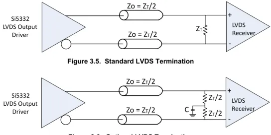
3.5.2 Differential Output Terminations LVDS Driver Termination
For a general LVDS interface, the recommended value for the differential termination impedance (ZT) is between 90 Ω and 132 Ω. The actual value should be selected to match the differential impedance (Z0) of the transmission line. A typical point-to-point LVDS design uses a 100 Ω parallel resistor at the receiver and a 100 Ω differential line environment. In order to avoid any transmission-line reflection issues, the components should be surface mounted and must be placed as close to the receiver as possible. The stand-ard LVDS termination schematic as shown in Figure 3.5 Standard LVDS Termination on page 12 can be used with either type of output structure. Figure 3.6 Optional LVDS Termination on page 12, which can also be used with both output types, is an optional termination with center tap capacitance to help filter common mode noise. The capacitor value should be approximately 0.01 to 0.1 μF. If using a non-standard termination, please contact Silicon Labs to confirm if the output structure is current source or voltage source type. In addition, since these outputs are LVDS compatible, the input receiver’s amplitude and common-mode input range should be verified for compatibility with the output.
Si5332 LVDS Output Driver
Zo = Z
T/2
+
-LVDS ReceiverZ
TZo = Z
T/2
Figure 3.5. Standard LVDS Termination
+
-LVDS ReceiverZ
T/2
Z
T/2
C
Zo = Z
T/2
Zo = Z
T/2
Si5332 LVDS Output DriverFigure 3.6. Optional LVDS Termination
Termination for 3.3 V LVPECL Outputs
The clock layout topology shown below is a typical termination for LVPECL outputs. The two different layouts mentioned are recom-mended only as guidelines. The differential outputs generate ECL/LVPECL compatible outputs. Therefore, terminating resistors (DC current path to ground) or current sources must be used for functionality. These outputs are designed to drive 50 Ω transmission lines. Matched impedance techniques should be used to maximize operating frequency and minimize signal distortion. Figure 3.7 3.3 V LVPECL Output Termination, Option 1 on page 13 and Figure 3.8 3.3 V LVPECL Output Termination, Option 2 on page 13 show two different layouts. Other suitable clock layouts may exist, and it would be recommended that the board designers simulate to guar-antee compatibility across all printed circuit and clock component process variations.
3.3V
3.3V
LVPECL
Zo=50Ω
Zo=50Ω
R1
50Ω
50Ω
R2
+
-
Input
Vcc-2V
RTT
RTT = 54Ω
Si5332 LVPECL Output DriverFigure 3.7. 3.3 V LVPECL Output Termination, Option 1
3.3V
3.3V
LVPECL
Zo=50Ω
Zo=50Ω
R1
84Ω
84Ω
R2
+
-
Input
R4
125Ω
R3
125Ω
3.3V
Si5332 LVPECL Output DriverFigure 3.8. 3.3 V LVPECL Output Termination, Option 2
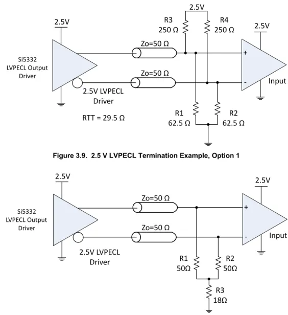
Termination for 2.5 V LVPECL Outputs
Figure 3.9 2.5 V LVPECL Termination Example, Option 1 on page 14 and Figure 3.10 2.5 V LVPECL Termination Example, Option 2 on page 14 show examples of termination for the 2.5 V LVPECL driver option. These terminations are equivalent to terminating 50 Ω to VDDO – 2 V. For VDDO = 2.5 V, the VDDO – 2 V is very close to ground level. The R3 in Figure 3.10 2.5 V LVPECL Termination Example, Option 2 on page 14 can be optionally eliminated using the termination shown in Figure 3.9 2.5 V LVPECL Termination Example, Option 1 on page 14.
2.5V
2.5V
2.5V LVPECL
Driver
Zo=50 Ω
Zo=50 Ω
R1
62.5 Ω
62.5 Ω
R2
+
-
Input
R4
250 Ω
R3
250 Ω
2.5V
RTT = 29.5 Ω
Si5332 LVPECL Output DriverFigure 3.9. 2.5 V LVPECL Termination Example, Option 1
2.5V
2.5V
2.5V LVPECL
Driver
Zo=50 Ω
Zo=50 Ω
R1
50Ω
50Ω
R2
+
-
Input
R3
18Ω
Si5332 LVPECL Output DriverFigure 3.10. 2.5 V LVPECL Termination Example, Option 2
Termination for HCSL Outputs
The Si5332 HCSL driver option integrated termination resistors to simplify interfacing to an HCSL receiver. The HCSL driver supports both 100 Ω and 85 Ω transmission line options. This configuration option may be specified using ClockBuilder Pro or via the device I2C interface.
1.425V to 3.63V
OUTx
OUTx
Zo=42.5Ω
or 50Ω
HCSL
receiver
Zo=42.5Ω
or 50Ω
Si5332
HCSL Output
Driver
Figure 3.11. HCSL Internal Termination Mode
1.425V to 3.63V
OUTx
OUTx
Zo=42.5Ω
or 50Ω
HCSL
receiver
Zo=42.5Ω
or 50Ω
R
T= Zo
R
T= Zo
Si5332
HCSL Output
Driver
Figure 3.12. HCSL External Termination Mode
3.5.3 LVCMOS Output Terminations
LVCMOS outputs can be dc-coupled, as shown in the figure below.
1.71 to 6.36V
OUTxb
OUTx
Zo=50Ω
Zo=50Ω
Set output driver
to 50Ω mode.
Figure 3.13. LVCMOS Output Termination Example, Option 1
1.425 to 3.63V
OUTxb
Rs
OUTx
Rs
Rs = Zo – Rdrv
(see Table 5.8)
Set output driver
to 25Ω mode.
Figure 3.14. LVCMOS Output Termination Example, Option 2
3.5.4 LVCMOS Output Signal Swing
The signal swing (VOL/VOH) of the LVCMOS output drivers is set by the voltage on the VDDO pin for the respective bank. 3.5.5 LVCMOS Output Polarity
When a driver is configured as an LVCMOS output it generates a clock signal on both pins (OUTx and OUTxb). By default, the clock on the OUTxb pin is generated in phase with the clock on the OUTx pin. The polarity of these clocks is configurable enabling complimenta-ry clock generation and/or inverted polarity with respect to other output drivers.
3.5.6 Output Enable/Disable
The universal hardware input pins can be programmed to operate as output enable (OEb), controlling one or more outputs. Pin assign-ment is done using ClockBuilder Pro. An output enable pin provides a convenient method of disabling or enabling the output drivers. When the output enable pin is held high all designated outputs will be disabled. When held low, the designated outputs will be enabled. Outputs in the enabled state can be individually disabled through register control.
3.5.7 Differential Output Configurable Skew Settings
Skew on the differential outputs can be independently configured. The skew is adjustable in 35 ps steps across a range of 245 ps.
Functional Description
3.6 Spread Spectrum
To help reduce electromagnetic interference (EMI), the Si5332 supports spread spectrum modulation. The output clock frequencies can be modulated to spread energy across a broader range of frequencies, lowering system EMI. The Si5332 implements spread spectrum using its patented MultiSynth technology to achieve previously unattainable precision in both modulation rate and spreading magnitude. Spread spectrum can be enabled through I2C, or by configuring one of the universal hardware input pins using ClockBuilder Pro. The Si5332 features both center and down spread spectrum modulation capability, from 0.1% to 2.5%. Each MultiSynth is capable of generating an independent spread spectrum clock. The feature is enabled using a user-defined universal hardware input pin or via the device I2C interface. Spread spectrum can be applied to any output clock derived from a MultiSynth fractional divider, with any clock frequency up to 250 MHz. Since the spread spectrum clock generation is performed in the MultiSynth fractional dividers, the spread spectrum waveform is highly consistent across process, voltage and temperature. The Si5332 features two independent MultiSynth di-viders, enabling the device to provide two independent spread profiles simultaneously to the clock output banks.
Spread spectrum is commonly used for 100 MHz PCI Express clock outputs. To comply with the spread spectrum specifications for PCI Express, the spreading frequency should be set to a maximum of 33 kHz and –0.5% down spread. A universal hardware input pin can be configured to toggle spread spectrum on/off.
3.7 Universal Hardware Input Pins
Universal hardware input pins are user configurable control input pins that can have one or more of the functions listed below assigned to them using ClockBuilder Pro.
Universal hardware input pins can be utilized for the following functions:
Table 3.2. Universal Hardware Input Pins Description Function
SSEN_EN0 Spread spectrum enable on MultiSynth0 (N0).
SSEN_EN1 Spread spectrum enable on MultiSynth0 (N1).
FS_INTx Used to switch an integer output divider frequency from frequency A to frequency B. FS_MSx Used to switch a MultiSynth output divider output from frequency and/or change spread
spectrum profile.
OE Output enable for one or more outputs.
I2C address select Sets the LSB of the I2C address to either 0 or 1. CLKIN_SEL[1:0] Selects between crystal or clock inputs.
Spread Spectrum Enable Pins (SSEN[1:0])
Spread_EN[1:0] pins are active pins that enable/disable spread spectrum on all outputs that correspond to MutliSynth0 or MultiSynth1, respectively. The change in frequency or spread spectrum will be instantaneous and may not be glitch free.
Table 3.3. SSEN_EN Pin Selection Table SSEN_ENx
0 Spread Spectrum disabled on MultiSynthx
1 Spread Spectrum enabled on MultiSynthx
Output Frequency Select Pins
There are five integer dividers, one corresponding to each of the five output banks. Using ClockBuilder Pro, a universal hardware input pin can be assigned for each integer divider, providing capability to select between two different pre-programmed divide values. Divider values of every integer from 8 to 255 are available in ClockBuilder Pro for each integer divider.
Table 3.4. FS_INT Pin Selection Table
FS_INTx Output Frequency from INTx
0 Frequency A, as defined in ClockBuilder Pro
1 Frequency B, as defined in ClockBuilder Pro
Output Enable
A universal hardware input pin can be defined to control output enable of a differential output, a bank of differential outputs, or as a global output enable pin controlling all outputs. Upon de-assertion of an OE pin, the corresponding output will be disabled within 2-6 clock cycles. Asserting an OE pin from disable to enable will take <20 µs for the output to have a clean clock.
Output enabled/disabled for LVCMOS are done in pairs. Each differential buffer True and Compliment output can generate an LVCMOS clock and the OE pin associated with the True and Compliment output buffer will control the respective LVCMOS pair. For example: If DIFF0 is configured to be SE1 and DIFF0# is configured to be SE2 and OE1 is the associated OE pin, de-asserting the OE1 pin will disable both SE1 and SE2 outputs. The disable and enable of the outputs to a known state is glitch free.
I2C Address Pin
This pin sets the LSB of the I2C address. For example, if the I2C address is A6h, setting this pin high will set the I2C address to A7h. CLKIN_SEL[0:1] Pins
These pins are used to set the input source clock between the input clock channels (Crystal, CLKIN_2/CLKIN_2# or CLKIN_3/ CLKIN_3#). Upon switching the input clock source, the output will not be glitch free. It is intended for the user to set this pin to a known state before the system is powered up or have the receiver address any unintended output signals when switching to a different input source clock.
Multi-Profile
Si5332 has the ability to store up to 16 unique configurations in the same custom part number by enabling multi-profile support in ClockBuilder Pro after selecting the desired Si5332 device. The ClockBuilder Pro wizard guides users to enter the input/output/feature set needed for each individual profile configuration, then compiles them together and assigns the necessary number of universal hard-ware pins based on the number of profiles entered.
3.8 Custom Factory Pre-programmed Parts
Custom pre-programmed parts can be ordered corresponding to a specific configuration file generated using the ClockBuilder Pro soft-ware utility. Silicon Labs writes the configuration file into the device prior to shipping. Use the ClockBuilder Pro custom part number wizard (http://www.silabs.com/clockbuilderpro) to quickly and easily generate a custom part number for your ClockBuilder Pro configu-ration file. A factory pre-programmed part will generate clocks at power-up.
In less than three minutes, you will be able to generate a custom part number with a detailed data sheet addendum matching your design’s configuration. Once you receive the confirmation email with the data sheet addendum, simply place an order with your local Silicon Labs sales representative. Samples of your pre-programmed device will ship within two weeks.
3.9 I2C Serial Interface
The Si5332 is compatible with rev6 of the I2C specification, including Standard, Fast, and Fast+ modes.
Configuration and operation of the Si5332 can be controlled by reading and writing registers using the I2C . Communication with a 1.8 V to 3.3 V host is supported. See the Si5332 Family Reference Manual for details.
3.10 In-Circuit Programming
The Si5332 is in-system configurable using the I2C interface by the following two methods:
• In-ciruit configuration of device registers after power-up. With this method changes to volatile register memory can be done as re-quired to produce the desired outputs. This does not alter internal NVM; therefore, register memory changes are lost at power-down. Refer to the Si5332 Family Reference Manual available on our web site for details.
• In-circuit re-configuration of internal NVM. Writing to internal NVM requires the use of the CBPro Field Programmer (CBPROG-DON-GLE) and CBPro software. See UG286: ClockBuilderPro Field Programmer Kit user's guide available on our web site for more infor-mation. (One important note: The Si5332 core VDDs (VDD_DIG, VDDA, and VDD_XTAL) must be powered by 3.3 V during in-circuit NVM programming.)
4. Register Map
Refer to the Si5332 Family Reference Manual for a complete list of registers descriptions and settings.
5. Electrical Specifications
Table 5.1. Recommended Operating Conditions
(VDD = VDDA = VDD_DIG = VDD_XTAL = 1.8 V to 3.3 V +10%/-5%, VDDO = 1.8 V ±5%, 2.5 V ±5%, or 3.3 V ±5%, TA = –40 to 85 °C) Parameter Symbol Test Condition Min Typ Max Units
Ambient Temperature TA –40 25 85 °C
Junction Temperature TJMAX — — 125 °C
Core Supply Voltage VDDA, VDD_DIG,
VDD_xtal
1.71 — 3.63 V
Output Driver Supply Voltage VDDO 1.425 — 3.63 V
Note:
1. All minimum and maximum specifications are guaranteed and apply across the recommended operating conditions. Typical val-ues apply at nominal supply voltages and an operating temperature of 25 °C unless otherwise noted.
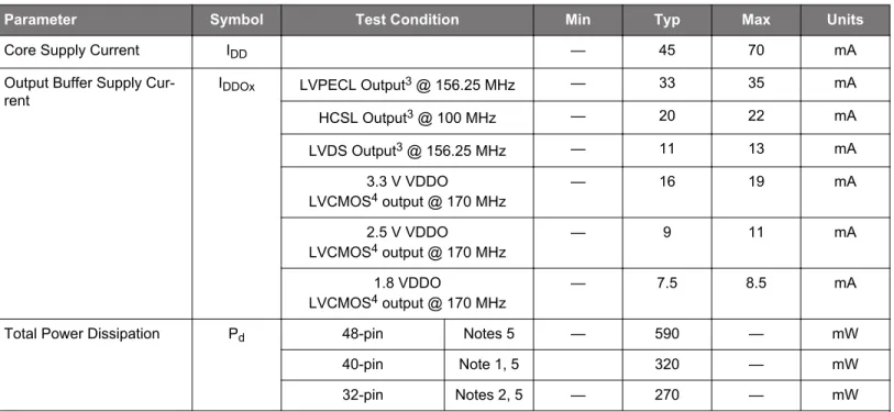
Table 5.2. DC Characteristics
(VDD = VDDA = VDD_DIG = VDD_XTAL = 1.8 V to 3.3 V +10%/-5%, VDDO = 1.8 V ±5%, 2.5 V ±5%, or 3.3 V ±5%, TA = –40 to 85 °C)
Parameter Symbol Test Condition Min Typ Max Units
Core Supply Current IDD — 45 70 mA
Output Buffer Supply
Cur-rent IDDOx LVPECL Output3 @ 156.25 MHz — 33 35 mA
HCSL Output3 @ 100 MHz — 20 22 mA LVDS Output3 @ 156.25 MHz — 11 13 mA 3.3 V VDDO LVCMOS4 output @ 170 MHz — 16 19 mA 2.5 V VDDO LVCMOS4 output @ 170 MHz — 9 11 mA 1.8 VDDO LVCMOS4 output @ 170 MHz — 7.5 8.5 mA
Total Power Dissipation Pd 48-pin Notes 5 — 590 — mW
40-pin Note 1, 5 320 — mW
32-pin Notes 2, 5 — 270 — mW
Notes:
1. Si5332 40-pin test configuration: VDDD = VDDA = VDDI = 1.8 V, 4 × 2.5 V LVDS outputs enabled @ 156.25 MHz, 2 × 1.8 V HCSL outputs enabled @ 100 MHz, 2x 3.3 V LVCMOS outputs enabled @ 25 MHz. . Excludes power in termination resistors.
2. Si5332 32-pin test configuration: VDDD = VDDA = VDDI = 1.8 V, 2 × 2.5 V LVDS outputs enabled @ 156.25 MHz, 2 × 1.8 V HCSL outputs enabled @ 100 MHz. 2x 3.3 V LVCMOS outputs enabled @ 25 MHz. Excludes power in termination resistors.
3. Differential outputs terminated into a 100 Ω load.
4. LVCMOS outputs measured into a 5 inch 50 Ω PCB trace with 4 pF load.
50 50 100 OUT OUT IDDO
Differential Output Test Configuration 5 inch
50 OUTa
IDDO
4 pF LVCMOS Output Test Configuration
5 inch
OUTb
5. Detailed power consumption for any configuration can be estimated using ClockBuilderPro when an evaluation board (EVB) is not available. All EVBs support detailed current measurements for any configuration.
Table 5.3. Clock Input Specifications
(VDD = VDDA = VDD_DIG = VDD_XTAL = 1.8 V to 3.3 V +10%/-5%, VDDO = 1.8 V ±5%, 2.5 V ±5%, or 3.3 V ±5%, TA = –40 to 85 °C)
Parameter Symbol Test Condition Min Typ Max Units
Input Clock (AC-coupled Differential Input Clock on CLKIN_2/CLKIN_2# or CLKIN_3/CLKIN_3#)
Frequency FIN Differential 10 — 250 MHz
Voltage Swing VPP_DIFF3 Differential AC-coupled
< 333.33 MHz 0.5 — 1.8 VPP_diff
Slew Rate SR/SF 20-80% 0.75 — — V/ns
Duty Cycle DC 40 — 60 %
Input Impedance RIN 10 — — kΩ
Input Capacitance CIN 2 3.5 6 pF
Input Clock (AC-coupled LVCMOS Input Clock on CLKIN_2 or CLKIN_3)
Frequency FIN 10 — 170 MHz
Input High Voltage VIH 0.8 × VDD — — V
Input Low Voltage VIL — — 0.2 × VDD V
Slew Rate1,2 SR/SF 20-80% 0.75 — — V/ns
Duty Cycle DC 40 — 60 %
Input Capacitance CIN 2 3.5 6 pF
Input Clock (AC-coupled Input Clock on XA)
Frequency FIN 10 — 170 MHz
Voltage Swing — 1 V
Input Low Voltage VIL — — 0.2 x VDD V
Slew Rate1, 2 SR/SF 20-80% 0.75 — — V/ns
Duty Cycle DC 40 — 60 %
Input Capacitance CIN 2 3.5 6 pF
Notes:
1. Imposed for jitter performance.
2. Rise and fall times can be estimated using the following simplified equation: tr/tf80-20 = ((0.8 - 0.2) * VIN_Vpp_se) / SR. 3. VPP_DIFF = 2 x VPP_SINGLE-ENDED
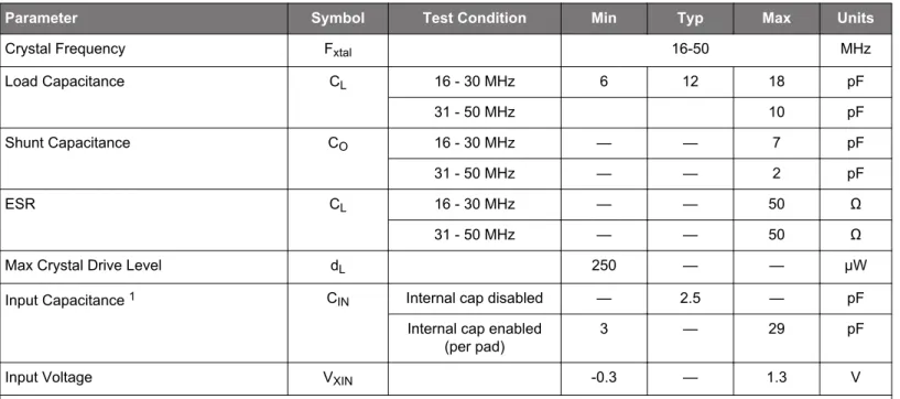
Table 5.4. External Crystal Input Specification
(VDD = VDDA = VDD_DIG = VDD_XTAL = 1.8 V to 3.3 V +10%/-5%, VDDO = 1.8 V ±5%, 2.5 V ±5%, or 3.3 V ±5%, TA = –40 to 85 °C)
Parameter Symbol Test Condition Min Typ Max Units
Crystal Frequency Fxtal 16-50 MHz
Load Capacitance CL 16 - 30 MHz 6 12 18 pF 31 - 50 MHz 10 pF Shunt Capacitance CO 16 - 30 MHz — — 7 pF 31 - 50 MHz — — 2 pF ESR CL 16 - 30 MHz — — 50 Ω 31 - 50 MHz — — 50 Ω
Max Crystal Drive Level dL 250 — — µW
Input Capacitance 1 CIN Internal cap disabled — 2.5 — pF
Internal cap enabled
(per pad) 3 — 29 pF
Input Voltage VXIN -0.3 — 1.3 V
Notes:
1. Internal capacitance on the xtal input pads is programmable or can be disabled. Please reference section 5.3.1 for more detailed information.
Table 5.5. Embedded Crystal Specifications
Parameter Symbol Test Condition Min Typ Max Units
Initial Accuracy1 fi Measured at +25 °C at
time of shipping — ±20 — ppm
Total Stability –50 — 50 ppm
Temperature Stability –30 — 30 ppm
Note:
1. Internal crystal loading capacitance is set at factory during device frequency calibration and can not be changed.
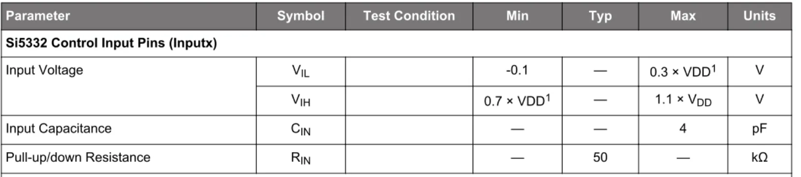
Table 5.6. Control Pins
(VDD = VDDA = VDD_DIG = VDD_XTAL = 1.8 V to 3.3 V +10%/-5%, or 3.3 V ±5%, TA = –40 to 85 °C)
Parameter Symbol Test Condition Min Typ Max Units
Si5332 Control Input Pins (Inputx)
Input Voltage VIL -0.1 — 0.3 × VDD1 V
VIH 0.7 × VDD1 — 1.1 × VDD V
Input Capacitance CIN — — 4 pF
Pull-up/down Resistance RIN — 50 — kΩ
Note:
1. VDD indicates all core voltages VDD_DIG, VDDA, and VDD_XTAL which are required to all be using same nominal voltage.
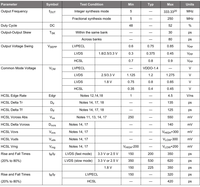
Table 5.7. Differential Clock Output Specifications
(VDD = VDDA = VDD_DIG = VDD_XTAL = 1.8 V to 3.3 V +10%/-5%, VDDO = 1.8 V ±5%, 2.5 V ±5%, or 3.3 V ±5%, TA = –40 to 85 °C)
Parameter Symbol Test Condition Min Typ Max Units
Output Frequency fOUT Integer synthesis mode 5 — 333.3320 MHz
Fractional synthesis mode 5 — 250 MHz
Duty Cycle DC 48 — 52 %
Output-Output Skew TSK Within the same bank — — 30 ps
Across banks — — 80 ps
Output Voltage Swing VSEPP LVPECL 0.6 0.75 0.85 VPP
LVDS 1.8/2.5/3.3 V 0.3 0.375 0.45 VPP
HCSL 0.7 0.8 0.9 VPP
Common Mode Voltage VCM LVPECL — VDDO-1.4 — V
LVDS 2.5/3.3 V 1.125 1.2 1.275 V
LVDS 1.8 V 0.75 0.8 0.85 V
HCSL 0.35 0.4 0.45 V
HCSL Edge Rate Edgr Notes 12,14,18 1 — 4.5 V/ns
HCSL Delta Tr Dtr Notes 14, 17, 18 — — 135 ps
HCSL Delta Tf Dtf Notes 14, 17, 18 — — 125 ps
HCSL Vcross Abs Vxa Notes 11, 13, 14, 17 250 — 550 mV
HCSL Delta Vcross Dvcrs Notes 14, 17 — — 140 mV
HCSL Vovs Vovs Notes 14, 17 — — VHIGH+300 mV
HCSL Vuds Vuds Notes 14, 17 — — VLOW-300 mV
HCSL Vrng Vrng Notes 14, 17 VHIGH-200 — VLOW+200 mV
Rise and Fall Times (20% to 80%)
tR/tF LVDS (fast mode) 3.3 V or 2.5 V 150 200 350 ps
LVDS (slow mode) 3.3 V or 2.5 V 350 530 620 ps
1.8 V 150 225 350 ps
Rise and Fall Times (20% to 80%)
tR/tF LVPECL 150 — 320 ps
HCSL — — 420 ps
Parameter Symbol Test Condition Min Typ Max Units Notes:
1. For best jitter performance, keep the midpoint differential input slew rate faster than 0.3 V/ns. 2. Not in PLL bypass mode.
3. For best jitter performance, keep the midpoint input single ended slew rate faster than 1 V/ns. 4. On chip termination resistance can be programmed on (100ohm) or off (high impedance). 5. Not including R divider.
6. Input capacitance on crystal pins targets 23 pf each plus 1 pf external trace capacitance to provide 12 pf series equivalent crystal load capacitance.
7. Measured at crossing point where the instantaneous voltage value of the rising edge of CLK equals the falling edge of CLK#. 8. Measure taken from differential waveform on a component test board. The edge (slew) rate is measured from -150mV to +150mV
on the differential waveform . Scope is set to average because the scope sample clock is making most of the dynamic wiggles along the clock edge Only valid for Rising clock and Falling Clock#. Signal must be monotonic through the Vol to Voh region for Trise and Tfall.
9. This measurement refers to the total variation from the lowest crossing point to the highest, regardless of which edge is crossing. 10. Test configuration is Rs=33.2 Ω, Rp=49.9, 2 pF.
11. Vcross(rel) Min and Max are derived using the following, Vcross(rel) Min = 0.250 + 0.5 (Vhavg 0.700), Vcross(rel) Max = 0.550 -0.5 (0.700 – Vhavg).
12. Measurement taken from Single Ended waveform.
13. Measurement taken from differential waveform VLow Math function. 14. Overshoot is defined as the absolute value of the maximum voltage. 15. Undershoot is defined as the absolute value of the minimum voltage.
16. The crossing point must meet the absolute and relative crossing point specifications simultaneously.
17. ΔVcross is defined as the total variation of all crossing voltages of Rising CLOCK and Falling CLOCK#. This is the maximum allowed variance in Vcross for any particular system.
18. Measured with oscilloscope, averaging off, using min max statistics. Variation is the delta between min and max.
OUTx OUTx Vpp_se Vpp_se Vpp_diff = 2*Vpp_se Vcm Vcm Vcm
19. LVDS swing levels for 50 Ω transmission lines. 20. Actually 333 + 1/3 MHz.
Table 5.8. LVCMOS Clock Output Specifications
(VDD = VDDA = VDD_DIG = VDD_XTAL = 1.8 V to 3.3 V +10%/-5%, VDDO = 1.8 V ±5%, 2.5 V ±5%, or 3.3 V ±5%, TA = –40 to 85 °C)
Parameter Symbol Test Condition Min Typ Max Units
Frequency fout 1.8-3.3 V CMOS 5 — 170 MHz
1.5 V CMOS 5 — 133.33 MHz Rise/Fall Time, 3.3 V (20-80%) tR/tF 50 Ω impedance, 5”trace, CL = 4 pf — 0.5 0.8 ns Rise/Fall Time, 2.5 V (20-80%) tR/tF 50 Ω impedance, 5”trace CL = 4 pf — 0.6 0.95 ns Rise/Fall Time, 1.8 V (20-80%) tR/tF 50 Ω impedance, 5”trace CL = 4 pf — 0.75 1.3 ns Rise/Fall Time, 1.5 V (20-80%) tR/tF 50 Ω impedance, 5”trace CL = 4 pf — 0.9 1.3 ns
CMOS Output Resistance
(Single Strength) 3.3 V — 46 — Ω
2.5 V — 48 — Ω
1.8 V — 53 — Ω
1.5 V — 58 — Ω
CMOS Output Resistance
(Double Strength) 3.3 V — 23 — Ω
2.5 V — 24 — Ω
1.8 V — 27 — Ω
1.5 V — 29 — Ω
CMOS Output Voltage VOH –4 mA load VDDO-0.3 — — V
VOL 4 mA load — — 0.3 V
Duty Cycle DC XO and PLL mode 45 — 55 %
Table 5.9. Performance Characteristics
(VDD = VDDA = VDD_DIG = VDD_XTAL = 1.8 V to 3.3 V +10%/-5%, VDDO = 1.8 V ±5%, 2.5 V ±5%, or 3.3 V ±5%, TA = –40 to 85 °C)
Parameter Symbol Test Condition Min Typ Max Units
Power Ramp tVDD 0 V to VDDmin 0.1 — 10 ms
Initialization Time tinitialization Time for I2C to become
operational after core supply exceeds VDDmin
— — 15 ms
Clock Stabilization from Power-up tSTABLE Time for clock outputs to
appear after POR — 15 25 ms
Input to Output Propagation Delay tPROP Buffer mode
(PLL Bypass)
— 2.5 4 ns
Spread Spectrum PP Frequency
Deviation SSDEV MultiSynth Output< 250 MHz 0.1 — 2.5 %
0.5% Spread Frequency Deviation SSDEV MultiSynth Output
< 250 MHz 0.4 0.45 0.5 %
Spread Spectrum Modulation Rate SSDEV MultiSynth Output
< 250 MHz 30 31.5 33 kHz
Notes:
1. Outputs at same frequencies and using the same driver format.
2. The maximum step size is only limited by the register lengths; however, the MultiSynth output frequency must be kept between 5 MHz and 250MHz.
3. Update rate via I2C is also limited by the time it takes to perform a write operation. 4. Default value is ~31.5 kHz.
Table 5.10. Jitter Performance Specifications
(VDD = VDDA = VDD_DIG = VDD_XTAL = 1.8 V to 3.3 V +10%/-5%, VDDO = 1.8 V ±5%, 2.5 V ±5%, or 3.3 V ±5%, TA = –40 to 85 °C)
Parameter Symbol Test Condition Typ Max Units
Jitter Generation,
Locked to External 25 MHz Clock
JGEN INT Mode
12 kHz – 20 MHz 1,2 210 280 fs RMS
FRAC/DCO Mode
12 kHz – 20 MHz 3,5 250 fs RMS
JPER Derived from integrated phase noise at a
BER of 1e-12 3.3 ps Pk-Pk
JCC 3.1 ps Pk
JPER N = 10, 000 cycles Integer or Fractional Mode. 2,3 Measured in the time domain. Performance is limited by the noise floor of
the equipment. 12 ps Pk-Pk JCC 11 ps Pk Jitter Generation, Locked to External 25 MHz Crystal
JGEN INT Mode
12 kHz – 20 MHz 1,2 190 240 fs RMS
FRAC/DCO Mode
12 kHz – 20 MHz 3,5 250 fs RMS
JPER Derived from integrated phase noise at a
BER of 1e-12 3.5 ps Pk-Pk
JCC 3.1 ps Pk
JPER N = 10, 000 cycles Integer or Fractional Mode. 2,3 Measured in the time domain. Performance is limited by the noise floor of
the equipment. 12 ps Pk-Pk JCC 11 ps Pk Jitter Generation, Locked to Embedded 50 MHz Crystal
JGEN INT Mode
12 kHz – 20 MHz 1,2 175 215 fs RMS
FRAC/DCO Mode
12 kHz – 20 MHz 3,5 250 fs RMS
JPER Derived from integrated phase noise at a
BER of 1e-1 3.2 ps Pk-Pk
JCC 2.8 ps Pk
JPER N = 10, 000 cycles Integer or Fractional Mode. 2,3 Measured in the time domain. Performance is limited by the noise floor of
the equipment.
12 ps Pk-Pk
JCC 11 ps Pk
Power Supply Noise Rejection6 PSNR 25 kHz –100 — dBc
50 kHz –97 —
100 kHz –72 —
500 kHz –83 —
1 MHz -91 —
Parameter Symbol Test Condition Typ Max Units Notes:
1. INT jitter generation test conditions fOUT = 156.25 MHz LVPECL.
2. Integer mode assumes that the output dividers (Nn/Nd) are configured with an integer value.
3. Fractional and DCO modes assume that the output dividers (Nn/Nd) are configured with a fractional value and the feedback divid-er is integdivid-er.
4. All jitter data in this table is based upon all output formats being differential. When LVCMOS outputs are used, there is the poten-tial that the output jitter may increase due to the nature of LVCMOS outputs. If your configuration implements any LVCMOS out-put and any outout-put is required to have jitter less than 3 ps RMS, contact Silicon Labs for support to validate your configuration and ensure the best jitter performance.
5. FRAC jitter generation test conditions fOUT = 150 MHz LVPECL.
6. Measured at 156.25 MHz carrier frequency. 100 mVpp sine wave noise added and noise spur amplitude measured.
Table 5.11. PCI-Express Clock Outputs (100 MHz HCSL)
(VDD = VDDA = VDD_DIG = VDD_XTAL = 1.8 V to 3.3 V +10%/-5%, VDDO = 1.8 V ±5%, 2.5 V ±5%, or 3.3 V ±5%, TA = –40 to 85 °C)
Parameter Test Condition SSC On/Off Typ Max Units
PCIe Gen 1.1 Includes PLL BW 1.5–22 MHz,
Peaking = 3dB, Td=10 ns, Ftrk=1.5 MHz with BER = 1E-12 2
Off 11 19 ps RMS
On 22 30 ps RMS
PCIe Gen 2.1 Includes PLL BW 5MHz & 8–16 MHz,
Jitter Peaking = 0.01-1 dB & 3 dB, Td=12ns, Low Band, F < 1.5 MHz
Off 0.016 0.023 ps RMS
On 0.12 0.21 ps RMS
Includes PLL BW 5 MHz & 8–16 MHz, Jitter Peaking = 0.01-1dB & 3dB, Td=12ns, High Band, 1.5 MHz < F < Nyquist2
Off 0.12 0.17 ps RMS
On 0.8 1.3 ps RMS
PCIe Gen 3.0
Com-mon Clock Includes PLL BW 2–4 MHz & 5 MHz, Peaking =0.01-2dB & 1dB, Td=12 ns, CDR = 10 MHz 2, 3
Off 0.037 0.048 ps RMS
On 0.26 0.35 ps RMS
PCIe Gen3.0 SRIS Includes PLL BW 4 MHz
Peaking = 2dB & 1dB, Td=12 ns CDR = 10 MHz 2, 3
On 0.35 0.41 ps RMS
PCIe Gen 4.0
Com-mon Clock Includes PLL BW 2–4 MHz & 5 MHz, Peaking =0.01-2dB & 1dB, Td=12 ns, CDR = 10 MHz 2, 3
Off 0.037 0.048 ps RMS
On 0.26 0.35 ps RMS
PCIe Gen4.0 SRIS Includes PLL BW 4 MHz
Peaking = 2dB & 1dB, Td=12 ns CDR = 10 MHz 2, 3
On 0.37 0.42 ps RMS
Notes:
1. All jitter data in this table is based upon all output formats being differential. When LVCMOS outputs are used, there is the poten-tial that the output jitter may increase due to the nature of LVCMOS outputs. If your configuration implements any LVCMOS out-put and any outout-put is required to have jitter less than 3 ps RMS, contact Silicon Labs for support to validate your configuration and ensure the best jitter performance.
2. All output clocks 100 MHz HCSL format. Jitter data taken from Clock Jitter Tool v.1.3. 3. Excludes oscilloscope sampling noise.
Table 5.12. Fanout Mode Additive Jitter Performance Specifications
(VDD = VDDA = VDD_DIG = VDD_XTAL = 1.8 V to 3.3 V +10%/-5%, VDDO = 1.8 V ±5%, 2.5 V ±5%, or 3.3 V ±5%, TA = –40 to 85 °C)
Parameter Symbol Test Condition Typ Max Units
Additive Phase Jitter 156.25MHz,
12kHz-20MHz1, LVDS (slow mode) 130 (LVDS slow) 170 fs RMS 156.25MHz, 12kHz-20MHz, LVDS (fast mode) 120 150 fs RMS 156.25MHz, 12kHz-20MHz, LVPECL1 110 140 fs RMS 156.25MHz, 12kHz-20MHz, HCSL1 120 150 fs RMS
PCIe Gen3 / 4
Addi-tive Phase Jitter 100MHz HCSL in-put/outputs
Includes PLL BW 2– 4 MHz, CDR = 10
MHz2, 3, 4, 5
28 36 fs RMS
Note:
1. Measured with differential input on CLKIN_2, bypassing the PLL to any output.
2. Silicon Labs PCIe Clock Jitter Tool is used to obtain measurements for additive phase jitter. Additive Phase Jitter = sqrt(output jitter2 - input jitter2). Input used is 100 MHz from Si5340.
3. Measurements on 100 MHz output use the template file in the PCIe Clock Jitter Tool. 4. For complete PCIe specifications, visit www.pcisig.com.
5. Input clock slew rate of 3.0 V/ns used for jitter measurements.
Table 5.13. Thermal Characteristics (Si5332A/B/C/D only)
Parameter Symbol Test Condition1 Value Units
Si5332 — 48 QFN
Thermal Resistance, Junction to Ambient θJA Still Air 25.5 °C/W
Air Flow 1 m/s 22.1
Air Flow 2 m/s 20.9
Thermal Resistance, Junction to Case θJC 14
Thermal Resistance, Junction to Board θJB 11.3
ψJB 11.0
Thermal Resistance, Junction to Top Center ψJT 0.4
Si5332 — 40 QFN
Parameter Symbol Test Condition1 Value Units
Thermal Resistance, Junction to Ambient θJA Still Air 25.6 °C/W
Air Flow 1 m/s 22.2
Air Flow 2 m/s 21.0
Thermal Resistance, Junction to Case θJC 14.1
Thermal Resistance, Junction to Board θJB 11.4
ψJB 11.1
Thermal Resistance, Junction to Top Center ψJT 0.4
Si5332 — 32 QFN
Thermal Resistance, Junction to Ambient θJA Still Air 32.8 °C/W
Air Flow 1 m/s 28.8
Air Flow 2 m/s 27.6
Thermal Resistance, Junction to Case θJC 18.5
Thermal Resistance, Junction to Board θJB 15.1
ψJB 14.9
Thermal Resistance, Junction to Top Center ψJT 0.5
Note:
1. Based on PCB Dimension: 3” x 4.5”, PCB Thickness: 1.6 mm, PCB Land/Via under GND pad: 36, Number of Cu Layers: 4. 2. Thermal characteristics for Si5332E/F/G/H for embedded crystal package options will be available soon.
Table 5.14. Absolute Maximum Ratings1,2,3
Parameter Symbol Test Condition Value Units
Storage Temperature Range TSTG –55 to +150 °C
DC Supply Voltage VDD –0.5 to 3.8 V
VDDA –0.5 to 3.8 V
VDDxtal –0.5 to 3.8 V
VDDO –0.5 to 3.8 V
Input Voltage Range VI XIN/XOUT –0.3 to 1.3 V
Latch-up Tolerance LU JESD78 Compliant
ESD Tolerance HBM 100 pF, 1.5 kΩ 2.0 kV
Junction Temperature TJCT –55 to 125 °C
Soldering Temperature TPEAK 260 °C
Soldering Temperature Time at TPEAK TP 20 to 40 sec
Notes:
1. Permanent device damage may occur if the absolute maximum ratings are exceeded. Functional operation should be restricted to the conditions as specified in the operational sections of this data sheet. Exposure to absolute maximum rating conditions for ex-tended periods may affect device reliability.
2. For more packaging information, go to www.silabs.com/support/quality/pages/RoHSInformation.aspx. 3. The device is compliant with JEDEC J-STD-020.
6. Pin Descriptions
6.1 Pin Descriptions (48-QFN) Input1 OUT10 OUT10b XA/CLKIN1 XB VDD_XTAL VDD_DIG VDDO5 OUT1 1 OUT1 1b Input6 OUT9 1 2 3 4 5 6 7 8 48 47 46 45 44 43 42 41 OUT7b OUT7 9 10 11 12 40 39 38 37 13 14 15 16 17 18 19 20 21 22 23 24 36 35 34 33 32 31 30 29 28 27 26 25OUT9b VDDO4 VDDO3
49 GND Input2 Input3 CLKIN_2 CLKIN_2b VDDA Input5 OUT6b OUT6 OUT5b OUT5 OUT4b OUT4 OUT3b OUT3 OUT1b OUT1 VDDO0
OUT0b OUT0 Input4
SCLK
SDA
TA
CLKIN_3 CLKIN_3b
VDDO1 OUT2b OUT2 VDDO2
OUT8b OUT8
Input7
Figure 6.1. 48-QFN
Table 6.1. Si5332 Pin Descriptions (48-QFN) Pin Number Pin Name Pin Type Function
1 VDD_DIG P Voltage supply for digital functions. Connect to 1.8–3.3 V. Part of internal
core VDD voltage. Must be connected to same voltage as VDDA and VDD_XTAL.
2 CLKIN_2 I These pins accept both differential and single-ended clock signals. Refer to
Section 3.4.2 Input Clocks for input termination options. These pins are high-impedance and must be terminated externally. If both the CLKIN_2 and CLKIN_2b inputs are un-used and powered down, then both inputs can be left floating. ClockBuilder Pro will power down an input that is set as "Un-used".
3 CLKIN_2b I
4 VDD_XTAL P Voltage supply for crystal oscillator. Connect to 1.8–3.3 V. Part of internal
core VDD voltage. Must be connected to same voltage as VDDA and VDD_XTAL.
5 XA/CLKIN1 I or P Si5332A/B/C/D:
These pins are used for an optional XTAL input when operating the device in asynchronous mode (i.e. free-run mode). Refer to Section 5. Electrical Specifications for recommended crystal specifications.
Si5332E/F/G/H (Embedded Crystal)
No Connect. Do not connect pins 5 or 6 to anything.
6 XB I or P
7 CLKIN_3 I These pins accept both differential and single-ended clock signals. Refer to
Section 3.4.2 Input Clocks for input termination options. These pins are high-impedance and must be terminated externally. If both the CLKIN_3 and CLKIN_3b inputs are unused and powered down, then both inputs can be left floating. ClockBuilder Pro will power down an input that is set as "Un-used".
8 CLKIN_3b I
9 VDDA P Core Supply Voltage. Connect to 1.8–3.3 V.
See the Si5332 Family Reference Manual for power supply filtering recom-mendations.
Must be connected to same voltage as VDD_DIG and VDD_XTAL.
10 INPUT1 I Universal HW Input pin. This hardware input pin is user definable through
ClockBuilder Pro. Refer to Section 3.7 Universal Hardware Input Pins for a list of definitions that hardware input pins can be used for.
11 INPUT2 I Universal HW Input pin. This hardware input pin is user definable through
ClockBuilder Pro. Refer to Section 3.7 Universal Hardware Input Pins for a list of definitions that hardware input pins can be used for.
12 INPUT3 I Universal HW Input pin. This hardware input pin is user definable through
ClockBuilder Pro. Refer to Section 3.7 Universal Hardware Input Pins for a list of definitions that hardware input pins can be used for.
13 SCLK I Serial Clock Input
This pin functions as the serial clock input for I2C.
SCLK is a digital input internally referenced to VDD_DIG. SCLK must have an external pull-up resistor (I2C bus pull-up) to same voltage as VDD_DIG.
Pin Descriptions
Pin Number Pin Name Pin Type Function
14 SDA I/O Serial Data Interface
This is the bidirectional data pin (SDA) for the I2C mode.
SDA is a digital open-drain bi-directional internally referenced to VDD_DIG. SDA must have an external pull-up resistor (I2C bus pull-up) to same volt-age as VDD_DIG.
15 OUT0b O Output Clock
These output clocks support a programmable signal swing and common mode voltage. Desired output signal format is configurable using register control. Termination recommendations are provided in 3.5.2 Differential Output Terminations and 3.5.3 LVCMOS Output Terminations. Unused out-puts should be left unconnected.
16 OUT0 O
17 VDDO0 P Supply Voltage (1.8–3.3 V, or 1.5 V for CMOS only) for OUT0
See the Si5332 Family Reference Manual for power supply filtering recom-mendations.
Leave VDDOx pins of unused output drivers unconnected. An alternate op-tion is to connect the VDDOx pin to a power supply and disable the output driver to minimize current consumption.
18 OUT1b O Output Clock
These output clocks support a programmable signal swing and common mode voltage. Desired output signal format is configurable using register control. Termination recommendations are provided in 3.5.2 Differential Output Terminations and 3.5.3 LVCMOS Output Terminations. Unused out-puts should be left unconnected.
19 OUT1 O
20 VDDO1 P Supply Voltage (1.8–3.3 V, or 1.5 V for CMOS only) for OUT1 and OUT2
See the Si5332 Family Reference Manual for power supply filtering recom-mendations.
Leave VDDOx pins of unused output drivers unconnected. An alternate op-tion is to connect the VDDOx pin to a power supply and disable the output driver to minimize current consumption.
21 OUT2b O Output Clock
These output clocks support a programmable signal swing and common mode voltage. Desired output signal format is configurable using register control. Termination recommendations are provided in 3.5.2 Differential Output Terminations and 3.5.3 LVCMOS Output Terminations. Unused out-puts should be left unconnected.
22 OUT2 O
23 INPUT4 I Universal HW Input pin. This hardware input pin is user definable through
ClockBuilder Pro. Refer to Section 3.7 Universal Hardware Input Pins for a list of definitions that hardware input pins can be used for.
24 VDDO2 P Supply Voltage (1.8–3.3 V, or 1.5 V for CMOS only) for OUT3, OUT4,
and OUT5
See the Si5332 Family Reference Manual for power supply filtering recom-mendations.
Pin Number Pin Name Pin Type Function
25 OUT3b O Output Clock
These output clocks support a programmable signal swing & common mode voltage. Desired output signal format is configurable using register control. Termination recommendations are provided in 3.5.2 Differential Output Ter-minations and 3.5.3 LVCMOS Output Terminations. Unused outputs should be left unconnected.
26 OUT3 O
27 OUT4b O Output Clock
These output clocks support a programmable signal swing & common mode voltage. Desired output signal format is configurable using register control. Termination recommendations are provided in 3.5.2 Differential Output Ter-minations and 3.5.3 LVCMOS Output Terminations. Unused outputs should be left unconnected.
28 OUT4 O
29 OUT5b O Output Clock
These output clocks support a programmable signal swing & common mode voltage. Desired output signal format is configurable using register control. Termination recommendations are provided in 3.5.2 Differential Output Ter-minations and 3.5.3 LVCMOS Output Terminations. Unused outputs should be left unconnected.
30 OUT5 O
31 OUT6b O Output Clock
These output clocks support a programmable signal swing & common mode voltage. Desired output signal format is configurable using register control. Termination recommendations are provided in 3.5.2 Differential Output Ter-minations and 3.5.3 LVCMOS Output Terminations. Unused outputs should be left unconnected.
32 OUT6 O
33 OUT7b O Output Clock
These output clocks support a programmable signal swing & common mode voltage. Desired output signal format is configurable using register control. Termination recommendations are provided in 3.5.2 Differential Output Ter-minations and 3.5.3 LVCMOS Output Terminations. Unused outputs should be left unconnected.
34 OUT7 O
35 OUT8b O Output Clock
These output clocks support a programmable signal swing & common mode voltage. Desired output signal format is configurable using register control. Termination recommendations are provided in 3.5.2 Differential Output Ter-minations and 3.5.3 LVCMOS Output Terminations. Unused outputs should be left unconnected.
36 OUT8 O
37 VDDO3 P Supply Voltage (1.8–3.3 V, or 1.5 V for CMOS only) for OUT6, OUT7,
and OUT8
See the Si5332 Family Reference Manual for power supply filtering recom-mendations.
Leave VDDOx pins of unused output drivers unconnected. An alternate op-tion is to connect the VDDOx pin to a power supply and disable the output driver to minimize current consumption.
38 INPUT5 I Universal HW Input pin. This hardware input pin is user definable through
ClockBuilder Pro. Refer to 3.7 Universal Hardware Input Pins for a list of definitions that hardware input pins can be used for.