A Study of Efficient Design and Evaluation
Methodology of Electrical and Electronic Equipment for EMC and Hardware Security in IoT Era
March, 2019
Yusuke Yano
Graduate School of
Natural Science and Technology (Doctoral Course)
OKAYAMA UNIVERSITY
Copyright c⃝ 2019 by Yusuke Yano All rights reserved.
Printed in Japan
Abstract
With the progress in internet of things (IoT), electromagnetic environment surround- ing the electrical and electronic equipment becomes worse than ever because electromag- netic interference (EMI) caused by conducted or radiated electromagnetic noise becomes larger due to increase in the operating frequency and the power consumption of integrated circuits and power converter circuits. Along with the increase in EMI, EMI regulation levels of various electromagnetic compatibility (EMC) standards become stringent. There- fore, EMC design to control the EMI and improve noise immunity of equipment becomes increasingly important.
Besides, the risk of security attacks such as unauthorized access, communication data eavesdropping and tampering, and service interruption has increased. Especially, hard- ware security (HWS) attacks such as side-channel attacks (SCAs) are concerned because IoT products are used indoors and outdoors and are open and easy to access physically.
SCA resistance criteria are regulated stringently by various organizations. Therefore, for equipment in IoT era, not only the EMC design but also HWS design to increase HWS attack resistance are important.
In addition, since the progress in IoT is growing rapidly, efficient EMC and HWS design is required simultaneously for adapting to the increase in production speed of IoT equipment. Generally, a product development process is driven in the order below:
specification development, system and functional design, hardware and software design, trial production, and performance evaluation. However, it is rare to finish these processes at once. Actually, the performance at first evaluation often does unsatisfy the required performance, workers will often do over again from the hardware and software design process. Since this rework causes delay in product development, a repetition of the rework should be avoided.
To prevent the repetition and to design efficiently, works which required an enormous amount of man-hours and costs (i.e. the trial production and the performance evaluation) should be omitted. To improve the efficiency in product development, it is necessary two things:
(A) predicting the product performance in the design process without going through the complete trial manufacture and performance evaluation process, and
(B) optimizing the product design without trial and error.
i
Solving these issues, (A) and (B), with computer-aided engineering (CAE) is a current trend. CAE tools are very powerful because they can reduce trial cost in product perfor- mance prediction and design optimization, but reflecting the characteristics of the entire product to the CAE tools is unrealistic in terms of calculation cost. Therefore, a simu- lation method of efficient EMC and HWS performance prediction is required to reduce the calculation cost. For the efficient simulation, it is important to construct high-speed analyzable models and to narrow down the analysis dimension and range. It is preferable that the number of man-hours for constructing the model is as small as possible, and ease of model building is important. In addition, since the performance of the model depends on the condition at the time of model construction, it is necessary to properly determine the condition. Besides, even if the CAE tool is used, it is difficult to optimize a compo- nent of product composed of plural elements. If plural elements can not be simultaneously optimized, the design and simulation processes are repeated. Therefore, an optimal de- sign method is also required. To optimize the plural elements, it is important to derive a function having the elements as a variable with respect to a criterion representing a target performance, and calculate the set of elements that satisfy the target. In deriving the function, it is practically impossible to use all the constituent elements as variables, so it is necessary to simplify the constituent elements. Since the accuracy of optimization and the application limit of optimum design depend on the simplification, appropriate simplification is important.
The objective of this thesis is establishing efficient EMC and HWS design methods realizing (A) and (B). As concrete methods to realize (A) and (B), three studies were investigated as follows:
• noise-source equivalent circuit modeling to predict conducted disturbance for real- izing (A) in EMC design,
• a study of SCA resistance estimation for realizing (A) in HWS design, and
• an optimal design method of snubber circuits (a kind of filters for suppressing EMI or information leakage) for realizing (B).
The abstracts of each study are described below.
Chapter 2 described a noise-source equivalent circuit model and a model identification method for realizing (A). A simple measurement system consisting of a data logger (or an oscilloscope) and general measurement probes was used to reduce the difficulty of model construction. In addition, as an appropriate condition of model construction, the model structure, the measurement method, and the measurement accuracy were examined. As a result, it was possible to estimate conduction disturbance with an error within 6 dB which can be said to be practically sufficient accuracy.
Chapter 3 described a study of a SCA resistance estimation for realizing (A). We examinated two methods: a SCA resistance evaluation method based on the signal-to- noise ratio (SNR) of the side-channel trace and a side-channel trace simulation method
Abstract iii using the EDA (electronic design automation) tool. For the former, the signal-to-noise ratio measurement method was shown. For the latter, a simpler and faster simulation method than the conventional method was shown. As a result, it showed that it can contribute to efficiency improvement of SCA resistance prediction.
Chapter 4 described an optimal design method of RL and RC snubber circuits in a case where the snubbers are applied to a synchronous buck converter for realizing (B). For optimization, the converter circuit was simplified with considering the inpedance magni- tude of components at the target frequency. It was shown that the optimum parameters can be analytically and uniquely determined by deriving the equation with the Q factor (objective function) and the snubber parameters (variables) in the simplified equivalent circuit.
Chapter 5 concludes that it is expected that the methods of Chapters 2–4 contribute to efficiency of EMC and hardware security design.
概要
IoT(Internet of Things)の進展に伴い,電気・電子機器の動作周波数や消費電力の増
加により,伝導電磁ノイズによるEMI(electromagnetic interference)が大きくなり,機 器周辺の電磁環境がこれまで以上に悪化している.それにより,EMC(electromagnetic
conpatibility)規格のEMI規制値が厳しくなっている.したがって,EMIを制御し,各機
器のノイズ耐性を向上させるEMC設計がこれまで以上に重要となる.
他方で,不正アクセス,通信データの盗聴や改ざん,サービスの中断などのセキュリ ティ攻撃のリスクが高まっている.特に,IoT製品は屋内外で使用され,オープンで物理 的なアクセスが容易なため,SCA(side-channel attack)のようなHWS(hardware security) 攻撃が懸念されている.SCA耐性基準は,様々な組織によって厳しく規制されている.し たがって,IoT時代の機器では,EMC設計だけでなく,HWS設計も重要であり,効率的 なHWS設計がEMC設計と同じ理由で同時に必要である.
さらに,IoTの進展は凄まじいため,IoT機器の生産速度の加速に対応するために効
率的なEMC/HWS設計も同時に要求される.一般的に,製品開発のプロセスは,設計,
試作,性能評価の順に実行される.しかし,これらのプロセスを一度で終えることは稀で あり,評価後の性能が要求性能を満足せず,設計プロセスからやり直すことが多い.この 手戻りは製品開発の遅れを引き起こすため,繰り返しは避けるべきである.
繰り返しを避け,効率的に設計するためには,膨大な工数とコスト(試作と性能評価)
を必要とする作業は省略すべきである.そのため,製品開発の効率化を図るためには,以 下の2つの実現が要求される.
(A) 製品の性能は試作および性能評価プロセスを経ることなく設計プロセスで予測する こと
(B) 試行錯誤なしに製品の設計を最適化すること.
CAE(computer aided engineering)ツールを用いてこれらの問題を解決することが現
代のトレンドである.CAEツールは,製品の性能予測や設計最適化において非常に強力 なツールであるものの,製品全体の特性をCAEツールに反映させることは,計算コスト の観点から現実的ではない.そのため,計算コストを削減するために,効率的なEMCと HWS性能の予測手法が求められる.効率的なシミュレーションのためには,解析範囲を 絞り込み,高速な解析モデルを構築することが必要である.モデル構築のための工数は可 能な限り少ない方が好ましく,モデル構築の容易さが重要である.また,モデルの性能は モデル構築時の条件に依存するため,条件を適切に決定する必要がある.CAEツールを 用いたとしても,複数の構成要素からなる回路やPCBの特性を最適に調整することは容
v
易ではない.複数のパラメータを同時に最適化できなければ,設計とシミュレーションの プロセスが繰り返されてしまう.そのため,最適設計手法の確立も同時に要求される.構 成要素を最適化するためには,目標の性能を表す指標に対して構成要素を変数に持つ関 数を導出し,目標を満たす構成要素の組を算出することが重要である.関数の導出におい て,構成要素の全てを変数とすることは現実的に不可能であるため,構成要素を簡略化す る必要がある.最適化の精度や最適設計の適用限界は簡略化の方法に依存するため,適切 な簡略化が重要である.
本研究の目的は,上記(A)と(B)の実現によるEMC/HWS設計の効率化である.そ のための具体的な方法として,次の3つを検討した.
• EMC設計において(A)を実現するための,伝導妨害を予測するノイズ源等価回路 モデルおよびその構築法
• HWS設計において(A)を実現するための,サイドチャネル攻撃耐性の予測手法
• EMCおよびHWS設計において(B)を実現するための,スナバ回路を最適に設計す る手法
2章では,(A)実現のために,ノイズ源等価回路モデルの同定法を提案した.この方法 では,モデル構築工数の削減のため,データロガー(もしくはオシロスコープ)と測定プ ローブで構成される非常に簡便な測定系を用いた.モデル構築の適切な条件として,モデ ル構造,測定方法,測定精度について検討した.その結果,実用上十分な精度と言える6 dB以内の誤差で伝導妨害波を推定することができた.
3章では,(A)実現のために,サイドチャネル攻撃耐性の予測手法を検討した.サイドチャ ネルトレースの信号対雑音比に基づくサイドチャネル攻撃耐性評価方法と,EDA(electronic
design automation)ツールを使用したサイドチャネルトレースシミュレーション方法につ
いて検討した.前者においては,信号対雑音比の測定方法を示した.後者においては,従 来の方法よりも簡易かつ高速にシミュレーション可能な方法を示した.その結果,サイド チャネル攻撃耐性予測の効率化に寄与できることを示した.
4章では,(B)実現のために,RLおよびRCスナバ回路を同期降圧型コンバータに適 用し,その最適設計法を提案した.最適化のために,ターゲット周波数における構成要素 のインピーダンスの大きさに着目し,コンバータ回路を簡略化した.さらに,簡略化した 等価回路において,Q値を目的関数とし,スナバパラメータを変数に持つ式を導出するこ とで,最適なパラメータを解析的かつ一意に決定できることを示した.
5章では,本研究で得られた知見をまとめ,本論文で示した手法がIoT時代における 電気電子機器のEMC/ハードウェアセキュリティ設計手法の効率化に有用であることを述 べた.
Acknowledgments
This thesis is a summary of my doctoral study in Electronic and Information Systems Engineering, Okayama University. I am grateful to a large number of people who have directly and indirectly helped me finish this work.
First of all, I would like to express my deep gratitude to Professor Yoshitaka Toyota who has granted me the chance to start this research and has given me innumerable advices and unrelenting encouragement. Thanks are extended to Professor Yasuyuki Nogami and Professor Eiji Hiraki who have given me much precious guidance on the course of this research. I am also deeply grateful to Assistant Professor Kengo Iokibe for his significant comments, advices, and delightful discussions which inspired many of the ideas in this thesis. I am also indebted to Dr. Tetsushi Watanabe in Industrial Technology Center of Okayama Prefecture for his impressive counsels and great insight. I am also deeply grateful to Professor Osami Wada for his significant comments, advices. My sincere thanks, going to Mr. Noriaki Kawanishi and Mr. Keiji Kino in GopherTec Inc. who supported us for precious support and helpful advice in research on side channel attacks.
I am also grateful to all present and past members of Optical and Electromagnetic Waves Laboratory, Okayama University. I particularity thank to the following members, who did much of the technical work and helped me overcome the difficulties encountered in my studies: Mr. Hiroki Geshi, Mr. Naoki Kawata, Mr. Yuhei Osaki, Mr. Yasunari Kumano, Mr. Toshiaki Teshima. I also appreciate the excellent secretarial services provided by Ms.
Midori Ohnishi and Ms. Yumiko Kurooka.
Finally, I would like to dedicate this thesis to my parents, Ms. Mikiko Yano and Mr.
Noboru Yano, in appreciation of their generous support and continuous encouragement.
vii
Contents
Abstract i
Abstract (in Japanese) v
Acknowledgments vii
1 General Introduction 1
1.1 Background . . . 1
1.2 Motivation . . . 2
1.3 Outline of Thesis . . . 5
2 Electromagnetic Noise Prediction Using Noise-source Equivalent Circuit Model for EMC Performance Evaluation 9 2.1 Introduction . . . 9
2.2 Existing Noise-source Equivalent Circuit Models . . . 11
2.3 Proposed Noise Source Equivalent Circuit Model . . . 14
2.3.1 Model Structure . . . 14
2.3.2 Parameter Identification Method . . . 15
2.4 Parameter Identification . . . 17
2.4.1 EUT and Measurement System . . . 17
2.4.2 Identified Model Parameters . . . 22
2.5 Conducted Disturbance Voltage Simulation . . . 25
2.5.1 Evaluation of Errors . . . 25
2.5.2 Consideration of Prediction Accuracy Decrease at High Frequencies 28 2.6 Another Application . . . 30
2.6.1 Model Structure and Parameter Identification Method . . . 31
2.6.2 Parameter Identification . . . 33
2.6.3 Conducted Disturbance Voltage Simulation . . . 35
2.7 Conclusion . . . 39
3 Side-channel Attack Resistance Estimation for Improvement of HWS Performance Evaluation 41 3.1 Introduction . . . 41
ix
3.2 Existing SCA Resistance Estimation Methods . . . 45
3.3 SCA Resistance Prediction Based on SNR of Side-channel Traces . . . 51
3.3.1 Definition of SNR of Side-channel Traces . . . 51
3.3.2 Prediction of Evaluation Criteria in Actual Attacks . . . 51
3.3.3 Proposed SNR Measurement Method . . . 52
3.4 Experimental Evaluation of Resistance Prediction Based on SNR . . . 53
3.4.1 Application and Measurement System . . . 53
3.4.2 Identification of Relationship Between Leakage Trace SNR and Cor- relation Coefficient . . . 58
3.5 Side-channel Trace Estimation Based on RTL Simulation . . . 64
3.5.1 Proposed Simulation Method . . . 64
3.5.2 Conversion Method from Measured Trace to Current Consumption 67 3.6 Simulated Trace Evaluation . . . 68
3.6.1 Application and Simulation Settings . . . 68
3.6.2 Comparison with Measured Traces . . . 72
3.6.3 CPA and MTD Results . . . 74
3.7 Conclusion . . . 76
4 Optimum Design Method of Snubber Circuit for Efficient EMC and HWS Design 79 4.1 Introduction . . . 79
4.2 Existing Optimal Design Methods of Snubber Circuits . . . 80
4.3 LC Resonance in Synchronous Buck Converter . . . 84
4.4 Proposed Method . . . 87
4.4.1 RL Snubber . . . 87
4.4.2 RC Snubber . . . 89
4.5 Identification of Potential Erros Due to Use of Simplified Equivalent Circuits 91 4.5.1 Observed Q Factor in SPICE Simulation . . . 91
4.5.2 Evaluation of Errors . . . 94
4.6 Evaluation of Negative Effects . . . 95
4.6.1 Overshoots . . . 95
4.6.2 Power Losses . . . 98
4.7 Conclusion . . . 100
5 General Conclusions 103
A Impedance Stabilization Network 105
Bibliography 112
Research Activities 113
Contents xi
Biography 119
List of Figures
1.1 Development processes of products: (a) general and (b) efficient. . . 3 1.2 Product development process with CAE analysis . . . 4 1.3 Outline of this thesis . . . 7 2.1 Diagrammatic illustration of system for measuring conducted disturbance
voltages. . . 14 2.2 Noise source equivalent circuit model. . . 15 2.3 Combined equivalent circuit of measurement system and noise-source equiv-
alent circuit model shown respectively in Fig. 2.1 and Fig. 2.2. . . 15 2.4 Configuration of system for measuring conducted disturbance voltages. . . 18 2.5 Time domain waveform of measured conducted disturbances and trigger
signals. . . 20 2.6 Spectral envelopes of measured voltage or current without EMI filter: (a)
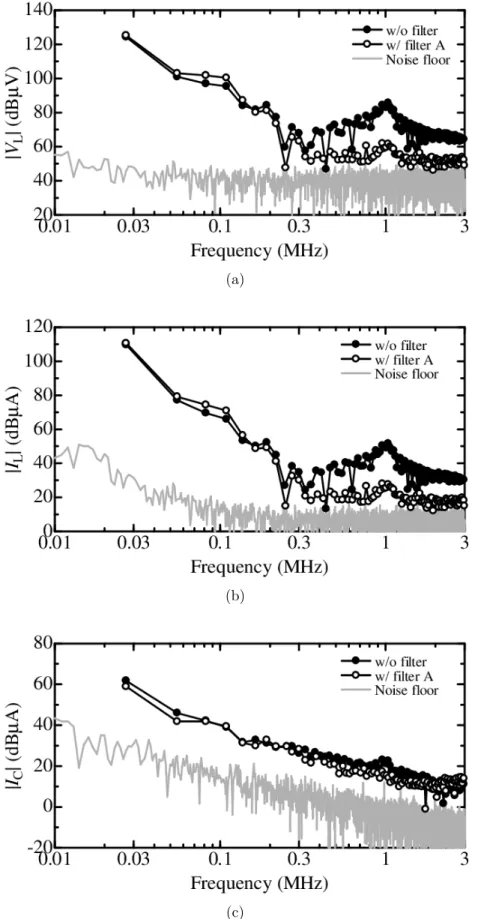
V˙L and ˙VN, (b) ˙IL and ˙IN, and (c) ˙IC. . . 21 2.7 Normal mode input impedance ˙ZIN−LISN looking leftward from terminal
pair L–N in Fig. 2.4. . . 23 2.8 Spectral envelopes of measured voltage or current under two conditions
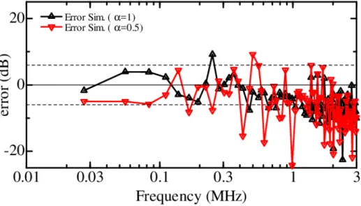
(without and with filterA): (a) ˙VL, (b) ˙IL, and (c) ˙IC. . . 24 2.9 Identified model parameters using α = 0.5 and α = 1: (a) ˙Zd, (b) ˙Id, (c)
Z˙c, and (d) ˙Vc. . . 26 2.10 Spectral envelopes of measured conducted disturbance voltage ˙VL without
filter and measured and simulated ˙VL with EMI filter B (4.4 µF). . . . 27 2.11 The errors between measured and simulated conducted disturbance voltages. 27 2.12 Identified model parameters usingα= 0,0.1,0.3,0.5,0.7,0.9, and1: (a) ˙Zd,
(b) ˙Id, (c) ˙Zc, and (d) ˙Vc. . . 29 2.13 Spectral envelopes of measured and simulated ˙VL for the different α. . . . . 30 2.14 Diagrammatic illustration of DC-DC converter. . . 31 2.15 Two-port noise source equivalent circuit model for DC-DC converter. . . . 32 2.16 DC-DC converter evaluation board and measurement points of conducted
disturbance. . . 33 2.17 Configuration of system for measuring conducted disturbance. . . 34 2.18 Spectral envelopes of measured voltage under three conditions (without
filters, with filters C, and with filters D): (a) ˙Vin and (b) ˙Vout. . . 36 xi
2.19 Spectral envelopes of simulated voltage with filters E: (a) ˙Vin and (b) ˙Vout. 37
2.20 Errors of spectral envelopes with filters E: (a) ˙Vin and (b) ˙Vout. . . 38
3.1 Appearance of SENPU (EUT-A): (a) component side and (b) solder side. . 55
3.2 Appearance of SASEBO (EUT-B): (a) component side and (b) solder side. 56 3.3 Measured traces and calculated correlation coefficients in EUT-A measure- ment: (a) for power rail probe and (b) for coaxial cable. . . 59
3.4 Variances of measured voltages at the target round with respect to change in the plaintext in EUT-A measurement. . . 60
3.5 Variation of the correlation coefficient by SNR and comparing with ones calculated by (3.3) in EUT-A measurement . . . 61
3.6 Measured trace and calculated correlation coefficient in EUT-B measurement 61 3.7 Variances of measured voltages at the target round with respect to change in the plaintext in EUT-B measurement. . . 62
3.8 Variation of the correlation coefficient by SNR and comparing with ones calculated by (3.3) in EUT-B measurement . . . 63
3.9 Flowchart of current consumption simulation . . . 65
3.10 Simulated dynamic current in RTL simulation . . . 66
3.11 FPGA model. . . 68
3.12 Equivalent circuit of EUT-A. . . 69
3.13 System layout for measuring Vmeas on EUT-A. . . 69
3.14 Transfer function K for converting from Vmeas to Isource. . . 70
3.15 Spectra of Vmeas calculated from Fig. 3.3(a). . . 71
3.16 Current spectra of Isource. . . 72
3.17 Isource for conparison with simulated trace. . . 73
3.18 Measured and simulated Isource with four values of ∆t: 8, 20.832, 4, 2 ns. . 74
3.19 MTD results of measured and simulated Isource. . . 75
4.1 Original equivalent circuit of synchronous buck converter. . . 84
4.2 Gate control signals used for SPICE simulation. . . 85
4.3 Simulated steady-state waveforms of characteristic voltagesVsd,HSandVds,LS w/o snubber circuits at (a) tOFF,HS and (b)tON,HS. . . 86
4.4 Simplified equivalent circuit of resonant loop excluding snubbers. . . 88
4.5 Simplified equivalent circuit of resonant loop including RL snubber. . . 88
4.6 Q factor contour plot drawn in accordance with (4.3) for use in optimally designing RL snubbers. . . 90
4.7 Simplified equivalent circuit of resonant loop including RC snubber. . . 90
4.8 Q factor contour plot drawn in accordance with (4.5) for use in optimally designing RC snubbers. . . 92
4.9 Spectral envelopes of simulated ringing waveformsVds,LS w/o and w/ opti- mized snubbers labeled D,IV for (a) RL snubber and (b) RC snubber. . . . 93
List of Fifures xiii 4.10 Q factors obtained from spectral envelopes of simulated ringing waveforms
with (a) optimized snubbers labeled A–G for different Q factor design tar- gets and (b) snubbers labeled I–VII for same Q factor design target. . . 94 4.11 Simulated steady-state waveforms of original equivalent circuit w/o and w/
optimized snubbers labeled D,IV: (a) surge voltage of Vsd,HSattOFF,HS and (b) inrush current of Is,HS attON,HS. . . 96 4.12 Simulated steady-state waveforms w/o and w/ optimized snubbers labeled
D,IV excluding waveforms shown in Fig. 4.11 for (a) and (b) RL snubber, and (c) and (d) RC snubber. . . 97 4.13 Calculated increases in surge voltages and inrush currents with (a) opti-
mized snubbers labeled A–G for different target Q factors and (b) snubbers labeled I–VII for same target. . . 98 4.14 Calculated steady-state power losses with (a) optimized snubbers labeled
A–G for different target Q factors and (b) snubbers labeled I–VII for same target. . . 100 A.1 Impedance stabilization network circuit including parasitic impedance. . . 105 A.2 Input impedance of impedance stabilization network: (a) magnitude and
(b) phase. . . 106
List of Tables
2.1 Features of general and existing methods for obtaining electrical character-
istics of circuit components and PCBs . . . 13
2.2 Specifications of System for Measuring Conducted Disturbance Voltages. . 18
2.3 EMI filter conditions and characteristics of leaded ceramic capacitors used as EMI filter. . . 22
2.4 Specifications of System for Measuring Conducted Disturbance. . . 34
2.5 Measurement Conditions and EMI filter Characteristics. . . 35
3.1 Features of existing methods for SCA resistance evaluation . . . 47
3.2 Features of existing methods for side-channel trace simulation . . . 50
3.3 EUTs used for examining validity of proposed SNR measurement method and SCA resistance evaluation based on SNR. . . 53
3.4 Specifications of System for Measuring SNR of Side-channel Traces on EUT-A. . . 57
3.5 Specifications of System for Measuring SNR of Side-channel Traces on EUT-B. . . 57
3.6 Common parameters in both SNR measurement. . . 58
3.7 List of Conditions for each SNR Measurement. . . 58
3.8 Power supply voltage settings for PPPA. . . 71
3.9 Peak-to-peak amplitude of each Isource shown in Fig. 3.18. . . 73
3.10 CPA result for each Isource shown in Fig. 3.18. . . 74
4.1 Features of existing methods for optimizing snubber circuits . . . 83
4.2 Switching Characteristics of Gate Control Signals . . . 85
4.3 Optimized Snubber Parameters Labeled A–G for Different Q Factor Design Targets and Parameters Labeled I–VII for Same Q Factor Design Target . . 93
4.4 Calculated Steady-state Power Losses in Original Equivalent Circuit w/o and w/ Optimized Snubber Circuits Labeled D,IV . . . 99
xv
Chapter 1
General Introduction
1.1 Background
With the progress in internet of things (IoT), various IoT devices (e.g., information terminals such as smartphone, sensors such as global positioning system and comple- mentary metal oxide semiconductor, etc.) are developed. The IoT devices provide a wide variety of services for consumer, commercial, industrial, and infrastrucure. For ex- ample, in consumer services, automobile driving services, energy management services such as smart home, etc., are provided. In commercial applications, medical and helth- care services, transportation services, etc., are provided. For developing those services, many technical topics are vigorously researched [1]. To realize those services, it is essen- tial to improve the performance of IoT devices. Improving the performance have been brought about by increased component density on printed circuit boards (PCBs), higher- speed switching speed of semiconductor devices, efficiency of data processing such as information-communication and cryptographic, etc..
In this situation, however, electromagnetic environment surrounding the electrical and electronic equipments becomes worse than ever because electromagnetic interference (EMI) caused by conducted or radiated electromagnetic noise becomes larger due to in- crease in the operating frequency and the power consumption of integrated circuits and power converter circuits. Along with the increase in EMI, EMI regulation levels of var- ious standards, e.g., VCCI (Voluntary Control Council for Interference by Information Technology Equipment), CISPR (Comit´e International Sp´ecial des Perturbations Ra- dio´electriques), etc., become stringent. Therefore, electromagnetic compatibility (EMC) design to control the EMI and improve noise immunity of equipments becomes increas- ingly important.
Besides, the risk of security attacks such as unauthorized access, communication data eavesdropping and tampering, and service interruption has increased. Especially, hard- ware security (HWS) attacks such as side-channel attacks (SCAs) [2] are concerned be- cause IoT products are used indoors and outdoors and are open and easy to access phys- ically. Recently, the vulnerability of CPUs to SCA has been reported [3, 4]. SCA resis-
1
tance criteria are regulated stringently by various organizations, e.g., IPA (Information- technology Promotion Agency) in Japan, NIST (National Institute of Standards and Technology) in the U.S.. Therefore, for equipment in IoT era, not only the EMC design but also HWS design to increase HWS attack resistance are important.
In addition, since the progress in IoT is growing rapidly, efficienct EMC design is required simultaneously.
1.2 Motivation
In IoT era, the quality and the efficiency of the EMC design and the HWS design are goes on important. Researches of this thesis examine methods to realize efficient EMC and HWS design. This subsection explains the motivation for the researches.
Fig. 1.1(a) shows a product development process. Generally, a product development process is driven in the order below: specification development, system and functional de- sign, hardware and software design, trial production, and performance evaluation. How- ever, it is rare to finish these processes at once. Actually, the performance at first eval- uation often does unsatisfy the required performance, engineers will often do over again from the hardware and software design process. Since this rework causes delay in product development, a repetition of the rework should be avoided.
To prevent the repetition and to design efficiently, works which required an enormous amount of man-hours and costs (i.e. the trial production and the performance evaluation) should be ommited. To improve the efficiency in product development, it is necessary two things:
(A) predicting the product performance in the design process without going through the complete trial manufacture and performance evaluation process, and
(B) optimizing the product design without trial and error.
The main objective of this thesis is to achieve (A) and (B) in the EMC and hardware security design. If (A) and (B) are ideally achieved, the design process will be the one shown in Fig. 1.1(b). The unnecessary man-hours and costs are reduced by achieving (A), and the reworks are reduced by achieving (B).
Solving these issues, (A) and (B), with computer-aided engineering (CAE) is a current trend. Fig. 1.2 shows a product development process containing CAE analysis. CAE tools are very powerful because they can reduce trial cost in product performance prediction and design optimization, but reflecting the characteristics of the entire product to the CAE tools is unrealistic in terms of calculation cost. Therefore, a simulation method of efficient EMC and HWS performance prediction is required to reduce the calculation cost.
For the efficient simulation, it is important to construct high-speed analyzable models and to narrow down the analysis dimension and range. Besides, even if the CAE tool is used, it is difficult to optimize a component of product composed of plural elements. If plural
1.2 Motivation 3
(a) (b)
Figure 1.1 Development processes of products: (a) general and (b) efficient.
elements can not be simultaneously optimized, the design and simulation processes are repeated. Therefore, a optimal design method is also required. To optimize the plural elements, it is important to derive a function having the elements as a variable with respect to a criterion representing a target performance, and calculate the set of elements that satisfy the target.
The objective of this thesis is establishing efficient EMC and HWS design methods realizing (A) and (B). For realizing (A) in the EMC design, this thesis investigates noise- source equivalent circuit modeling to predict conducted disturbances (a type of EMI) caused by power convertor circuits. Power converter circuits are implemented all sorts of electronic equipments and are the cause of large EMI. The noise source equivalent circuit model is a model that can analyze noise characteristics quickly by narrowing down the analysis target to only noise. For realizing (A) in the HWS design, this thesis focuses a SCA to a field-programmable gate array (FPGA) and investigates a SCA resistance estimation method. FPGA is a highly versatile integrated circuit, and it is implemented in various equipment including cryptographic equipment. For establishing the estimation method, we examined two topics: an SCA resistance evaluation method based on the SNR of side-channel traces and an efficient side-channel trace simulation method using
Figure 1.2 Product development process with CAE analysis
an electronic design automation (EDA) tool. There is a problem that the results of the existing SCA resistance evaluation can not be fed back to the electric circuit design because the existing evaluation criteria are different from the circuit design criteria. To solve this problem, this work focus on the SNR which is applicable to both criteria of the SCA resistance evaluation and the circuit design. The simulation method used here is a method to predict the side channel trace at high-speed by narrowing down design information used in the prediction. For realizing (B), this thesis focuses snubber circuits which are widely known filter to dump resonances and investigates thier optimal design method. Since resonances occur in all sorts of electronic equipments and increase the EMI
1.3 Outline of Thesis 5 and information leakage, a optimal design method is required. Here, the snubber circuits are optimized by using the Q factor which expresses the sharpness of resonance.
As preliminary before describing details of these investigations, issues of existing meth- ods and objectives of the investigations are explained in section 2 of each chapter.
1.3 Outline of Thesis
Figure 1.3 shows the outline of this thesis.
Chapter 2 described a noise-source equivalent circuit model and a model identification method for realizing (A). The model has two elements: equivalent sources and equivalent impedances representing respectively high-frequency current generated by switching de- vices and current leakage paths. The model parameters are identified only from external conducted disturbances (measured with an oscilloscope or a data logger) using circuit equations for the equivalent circuit including measurement system. The feature of this modeling method is that measurements using weak signals for modeling like the existing methods are not required. This feature make it possible to model large power equipments which were out of the application of the existing methods. Moreover, since the dedicated PCB and the advanced analysis are not used in model identification, it can be expected that the workload is reduced. The method proposed here is developed to eliminate two potential reasons for the reduced conducted disturbance simulation accuracy in previous works. The first is that part of the current was not represented in the previous model due to a balanced bridge circuit formed by the model and the measurement system. The second is that the measurement data used for parameter identification was not linearly independent because the circuit conditions were improperly changed during measurement.
The model was applied to an induction heating cooker having a versatile power converter circuit, and the errors in the conducted disturbance simulation were evaluated.
Chapter 3 described a study of a SNR estimation method in side-channel analysis for realizing (A). For establishing it, this work is examined two topics: an SCA resistance eval- uation method based on the SNR of side-channel traces and an efficient side-channel trace simulation method using an electronic design automation (EDA) tool. Firstly, this work has experimentally verified whether measured SNRs and correlation coefficients satisfy the analytical relationship. Since existing SCA resistance evaluation criteria are different from the circuit design criteria, there is a problem that the results of the existing evalu- ation can not be fed back to the electric circuit design. To solve this problem, this work focus on the SNR of side-channel traces. The SNR is commonly used as a design criterion in the circuit design, and the existing SCA resistance criteria can be predicted from the SNR. That is, if the SNR and the correlation coefficients can be accurately calculated, the SNR can be used for both the determination of countermeasure design targets and evaluation of the SCA resistance. Here, a method to measure the SNR accurately is pro- posed for experimental verification. The SNR was calculated using a signal component
obtained from the trace when encrypting a random plaintext set and a noise component obtained from the trace when encrypting a constant plaintext set, and the correlation coefficient was calculated based on the CPA. A PCB having an FPGA implemented an AES circuit was used as an EUT, and the core power supply voltage fluctuation of the FPGA on the PCB was measured as side-channel trace. The SNR was varied by chang- ing measurement conditions, measurement system, and EUTs, and the relationship was examined. Secondly, this work has proposed a side-channel trace simulation method us- ing EDA tools and has investigated whether the estimated traces have the side-channel information. Here, the current consumption of a cryptographic device during encryption is calculated as the side-channel traces. The current is estimated only from the damp file, which is generated by register transfer level (RTL) simulation, using a power consumption analyzing function of an EDA tool. Since detailed design information such as propagation delay is not included in the dump file generated here, the calculation cost is reduced as compared with the conventional methods. The fluctuations of the current with respect to the random plaintext set were estimated and compared with the measured one.
Chapter 4 described an optimal design method of RL and RC snubber circuits in a case where the snubbers are applied to a synchronous buck converter for realizing (B).
The method proposed here optimizes simultaneously two electronic components of the RL or RC snubber. To determine optimum snubber parameters analytically and uniquely, a contour plot drawn by a formula for the Q factor as a function of the snubber parameters derived from a simplified equivalent circuit of the resonant loop is used. The Q factor is a parameter that describes how underdamped an resonance is, and it is often used for design target in EMC design. The effects of the snubbers optimized using this method were reproduced by SPICE simulation to validate the method from the perspective of resonance damping, overshoot and power loss. The results showed that the damping effects obtained with the optimized snubbers met the Q factor design targets. They also demonstrate that the parameters are optimum in terms of suppressing overshoot and power loss. These results indicate that the method is suitable for optimizing RL and RC snubbers to damp parasitic LC resonance. The method proposed here is expected to be applied to other circuits because the contour plot can be drawn by any circuit if any objective function is just decided. This means that the proposed method is an efficient EMC and HWS design method.
Chapter 5 concludes this thesis with a summary of the key points.
1.3 Outline of Thesis 7
Figure 1.3 Outline of this thesis
Chapter 2
Electromagnetic Noise Prediction Using Noise-source Equivalent
Circuit Model for EMC Performance Evaluation
2.1 Introduction
The operating frequency of power converter circuits in electronic equipment is increas- ing due to the need for higher power efficiency and smaller electronic devices. Reducing electromagnetic interference (EMI) has thus become more important, and filters for sup- pressing EMI are required. To efficiently design such filters, a method is needed for quickly predicting EMI with high accuracy. Limits on the EMI generated in household appliances were established by CISPR 14-1 [40], and various noise source models have been developed for quickly predicting EMI [7–11].
Several noise source equivalent circuit models representing conducted disturbances caused by semiconductor device switching have been proposed [7–11]. Some of them [7–9]
have equivalent current sources and equivalent linear circuit elements. The equivalent current sources represent the high-frequency current generated by the nonlinear switch- ing operation of the semiconductor devices, and the equivalent linear circuit elements represent the impedances of the EMI leakage paths. A recently reported equivalent volt- age source model consisting of voltage sources representing the voltage variations caused by device switching and of impedances [10] has a circuit structure similar to those of previously reported models [7–9]. Moreover, a model has been reported that consists of elements having functions representing the state transitions of semiconductor devices and the impedances [11]. These circuit models enable the prediction of EMI and power quality deterioration. Constructing such models (e.g., [7–11]) requires information on the impedance characteristics of the semiconductor devices, circuit components, and printed circuit boards (PCBs) of the equipment under test (EUT). However, obtaining these
9
impedance characteristics may involve a lot of work. Models of the semiconductor devices and the electrical characteristics of the circuit components may not be available from the manufacturers, so measurements may need to be made. To obtain the electrical charac- teristics of the PCBs, measurement using a vector network analyzer (VNA) or simulation using an electromagnetic field analysis simulator is generally used. However, such mea- surement requires that the PCBs having dedicated patterns and dedicated terminals are needed to connect the measurement probes, increasing the workload. Furthermore, as PCBs become larger and more complicated, a greater amount of analysis time following simulation is needed.
A method for reducing the increase in workload has been proposed [12]. The impedance characteristics of the EUT are identified by inputting and outputting the input and out- put signals of a VNA into and from the EUT through current probes. With this method, changes to the system such as adding dedicated terminals are not needed for measure- ment, and the combined impedance of the semiconductor devices, circuit elements, and PCBs are obtained. However, if the EUT consumes a large amount of power, the noise it generates is much greater than the signal output from the VNA, making it difficult to measure the impedance characteristics with sufficient accuracy.
In this paper, we present a noise source equivalent circuit model and a model parameter identification method that are effective even in the large power consumption of the EUT.
It is intended to complement the existing method. While the elements in the circuit model (equivalent power sources and equivalent impedances) are similar to those in previously proposed models [7–9], the method for identifying model parameters is different. The parameters are identified from circuit equations of the overall equivalent circuit (including a model of the EUT and the measurement system) and external conducted disturbances measured with a measuring instrument (e.g. an oscilloscope or a data logger). Since only the external measurement data are used (and not an injected signal), it is possible to identify the model parameters when the power consumption of the EUT is large although it is difficult to identify them at frequencies with low power consumption.
In previous work [13, 15], we examined a method for predicting the conducted distur- bance voltage. A tabletop induction heating (IH) cooker with a general power converter circuit was used as the EUT. The method accurately predicted conducted disturbances under no-EMI-filter conditions but not under EMI-filter conditions. Subsequent work identified two potential reasons for the reduced accuracy and the method proposed here was developed to eliminate them. The first reason is that part of the current was not represented in the model used due to a balanced bridge circuit formed by the model impedance and the measurement system impedance. The second reason is that the mea- surement data used for model parameter identification was not linearly independent due to the way that the circuit conditions were changed during measurement was improper.
The rest of the paper is organized as follows. Section 2.2 introduces existing noise source equivalent circuit models and an objective of this research. Section 2.3 introduces the structure of the noise source equivalent circuit model and the method for identifying
2.1 Introduction 11 the model parameters. Section 2.4 describes their application in a system for measuring the conducted disturbance voltage and presents the identified parameters. Section 2.5 describes the simulation of the conducted disturbance voltage and discusses the error.
Section 2.7 concludes the paper with a summary of the key points.
2.2 Existing Noise-source Equivalent Circuit Models
Reducing EMI has become more important, and carefully designed filters and PCBs for suppressing EMI are required. To efficiently design them, a method is needed for quickly predicting EMI with high accuracy because, as (A) described in Section 1.2, reflecting the characteristics of the entire product to CAE tools is unrealistic in terms of calculation cost. In [5, 6], an circuit operation and an EMI are simulated by using models that faithfully express switching devices and a circuit configuration of a power conversion circuit including paracitic impedances. However, these simulation modeling is inefficient because it is necessary to model one each device and circuit pattern particularly, it is difficult and time-consuming.
Several noise source equivalent circuit models have been proposed for representing con- ducted disturbances caused by semiconductor device switching [7–11]. Some of them [7–9]
have equivalent current sources and equivalent linear circuit elements. The equivalent cur- rent sources represent the high-frequency current generated by the nonlinear switching operation of the semiconductor devices, and the equivalent linear circuit elements repre- sent the impedances of the EMI leakage paths. A recently reported equivalent voltage source model consisting of voltage sources representing the voltage variations caused by device switching and of impedances [10] has a circuit structure similar to those of pre- viously reported models [7–9]. Moreover, a model has been reported that consists of elements having functions representing the state transitions of semiconductor devices and the impedances [11]. These circuit models enable the prediction of EMI and power qual- ity deterioration. These models express only the noise generated in electric circuits and do not express the circuit operation, so that the modeling difficulty decreases because it is not necessary to know structure details of a target circuit to be modeled compared with [5, 6]. This means that these models can simulate EMI even when detail information of circuit components is not available form the manufacturers. These models are models that can analyze noise characteristics quickly by narrowing down the analysis target to only noise.
Constructing such models (e.g., [7–11]) requires information on the impedance char- acteristics of a modeling target circuit and leakage noise. Unfortunately, obtaining these impedance characteristics may involve a lot of work. To obtain the electrical charac- teristics of the circuit components and the PCBs, simulation using an EM simulator or measurement using a vector network analyzer (VNA) is generally used. Table 2.1 shows features of these general methods and an existing method for reducing measurement
costs [12].
In the simulation using an EM simulator, the impedance extraction cost is extremely high. As PCBs become larger and more complicated, a greater amount of analysis time following simulation is needed. Furthermore, it is impractical to apply that to the EUT in operation. This is because an immense amount of analysis time is needed and models of all circuit components are required.
In the measurement using a VNA and dedicated PCBs, the impedance extraction cost is high. PCBs having dedicated patterns and dedicated terminals are required to connect the measurement probes of a VNA. This method has a limitation when applied to the EUT in operation. If the EUT consumes a large amount of power, the noise it generates is much greater than the signal output from the VNA, making it difficult to measure the impedance characteristics with sufficient accuracy.
A method have been proposed to reduce the impedance extraction cost in the general measurement method [12]. This method uses a VNA and current probes. Owing to contactless probing, no change in the dedicated board and the measurement system is required, thereby reducing the impedance extraction cost. However, this method is limited to small consumption EUTs for the same reason as the general measurement method.
This thesis proposed a noise source equivalent circuit model and a model parameter identification method that are effective even in large power consumption of the EUT.
The model has two elements: equivalent sources and equivalent impedances representing respectively high-frequency current generated by switching devices and current leakage paths. The model parameters are identified only from external conducted disturbances (measured with an oscilloscope or a data logger) using circuit equations for the equiva- lent circuit including measurement system. The feature of this modeling method is that measurements using weak signals for modeling like the existing methods are not required.
This feature make it possible to model large power equipments which were out of the ap- plication of the existing methods. Moreover, since the dedicated PCB and the advanced analysis are not used in model identification, it can be expected that the workload is reduced. The method proposed here is developed to eliminate two potential reasons for the reduced conducted disturbance simulation accuracy in previous works [13–15]. The first is that part of the current was not represented in the previous model due to a bal- anced bridge circuit formed by the model and the measurement system. The second is that the measurement data used for parameter identification was not linearly independent because the circuit conditions were improperly changed during measurement. Details of investigations are described in Chapter 2.
2.1 Introduction 13
Table2.1FeaturesofgeneralandexistingmethodsforobtainingelectricalcharacteristicsofcircuitcomponentsandPCBs GeneralmethodsExistingmethodProposedmethod Requirement SimulationusinganEM simulatorMeasurementusinga VNAanddedicated PCBs Measurementusing aVNAandcurrent probes[12]
Measurementusinga OSCandmeasurement probes Impedance extractioncostHighHighLowLow (AsPCBsbecomelarger andmorecomplicated, agreateramountof analysistimefollowing simulationisneeded.)
(thePCBshavingdedi- catedpatternsandded- icatedterminalsarere- quiredtoconnectthe measurementprobes.) (Owingtocontactless probing,nochangein thededicatedboardand themeasurementsys- temisrequired.)
(Owingtouseof measurementequip- mentsgeneralyused inEMImeasurement, nochangeintheded- icatedboardandthe measurementsystemis required.) Applicationto EUTinoperationImpracticalLimitedUnlimited (Animmenseamount ofanalysistimeis needed.Modelsofall circuitcomponentsare required.)
(IftheEUTconsumesalargeamountof power,thenoiseismuchgreaterthanthe signaloutputfromtheVNA,makingitdif- ficulttomeasuretheimpedancecharacteris- ticswithsufficientaccuracy.) (Sincemeasurements usingweaksignalsfor modelingliketheex- istingmethodsarenot required,itispossible tomodellargepower equipments.)
Figure 2.1 Diagrammatic illustration of system for measuring conducted disturbance voltages.
2.3 Proposed Noise Source Equivalent Circuit Model
Fig. 2.1 shows a diagrammatic illustration of the system specified in CISPR 16-2-1 [41]
for measuring conducted disturbance voltages. The EUT is connected to a commercial power supply via a line impedance stabilization network (LISN). An EMI filter is mounted on the EUT. ˙VL and ˙VN represent the conducted disturbance voltages, which are high- frequency voltages from the L and N phases of the EUT port to the system ground, respectively. ˙IL and ˙IN represent normal mode currents flowing along each phase of the EUT port. CP is the parasitic capacitance between the EUT and the system ground. ˙IC
represents a common mode current flowing through the loop consisting of CP, the EUT, power cables, the LISN, and the system ground.
2.3.1 Model Structure
Previously reported models [7–11, 13, 15] have equivalent source elements representing the high-frequency currents generated by the nonlinear switching activity of the semicon- ductor devices and equivalent linear circuit elements representing the impedances of the EMI leakage paths. The model proposed here has the same structure.
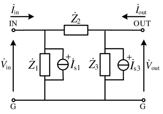
Fig. 2.2 shows the noise source equivalent circuit model. ˙Id is the equivalent current source representing the high-frequency current generated by an EUT switching device.
Z˙d is the equivalent impedance for the normal mode impedance of the EUT. ˙Zc is the equivalent impedance for the common mode impedance. V˙c is the equivalent voltage source representing the electromotive force that generates the common mode current.
The coefficient α of ˙Id and ˙Zd is an unbalance factor representing the unbalance of the normal mode elements across node A.
2.3 Proposed Noise Source Equivalent Circuit Model 15
Figure 2.2 Noise source equivalent circuit model.
Figure 2.3 Combined equivalent circuit of measurement system and noise-source equiv- alent circuit model shown respectively in Fig. 2.1 and Fig. 2.2.
2.3.2 Parameter Identification Method
The parameters are identified from circuit equations of the overall equivalent circuit (including a model of the EUT and the measurement system) and external conducted disturbances measured with a measuring instrument (e.g. an oscilloscope or a data logger).
Fig. 2.3 shows the equivalent circuit for the case in which the model shown in Fig. 2.2 is applied to the EUT portion of the measurement system shown in Fig. 2.1. The right side of port L–N is the proposed noise source model and the left side is the EMI filter and the LISN. ˙ZL and ˙ZNare the equivalent impedances between the EUT side terminals and
the ground terminal of the LISN. ˙ZF is the impedance of the EMI filter. ˙VL, ˙VN, ˙IL, ˙IN and ˙IC correspond to those in Fig. 2.1. The model parameters are identified using these voltages and currents, which are measurable outside the EUT. ˙IF is defined as the current flowing through ˙ZF and is calculated using
I˙F = ( ˙VL−V˙N)/Z˙F. (2.1) The circuit equations of the equivalent circuit shown in Fig. 2.3 are derived for model parameter identification. Application of Kirchhoff’s voltage law to loops 1 and 2 (shown by the dashed lines in Fig. 2.3) gives the equations:
[ V˙L V˙N
]
=
[ −1 I˙L−I˙F 0 0 1 −I˙C 0 0 1 I˙F−I˙N 1 −I˙C
]
−α2Z˙dI˙d αZ˙d (1−α)2Z˙dI˙d
(1−α) ˙Zd V˙c Z˙c
. (2.2)
The model parameters are determined in accordance with (2.2).
The equations (2.2) are the simultaneous quadratic equations with five unknowns ( ˙Zd, ˙Id, ˙Zc, ˙Vc, and α). To solve the equations, the coefficient α is determined before identifying the model parameters. When αis determined, the equations (2.2) become the simultaneous linear equations with four unknowns as shown below, and they can be easily solved.
[ V˙L V˙N
]
=
[ −α2 α( ˙IL−I˙F) 1 −I˙C (1−α)2 (1−α)( ˙IF−I˙N) 1 −I˙C
]
Z˙dI˙d
Z˙d V˙c Z˙c
. (2.3)
The coefficientαmust be carefully determined because the value ofαaffects the accuracy of model parameter identification. In our previous work [15], we assumed that the common mode current flowing through the EUT flows equally to terminals L and N. We thus set α to 0.5 to make the two normal mode impedances (αZ˙d and (1−α) ˙Zd) equal. However, setting α to 0.5 creates a problem: a state in which part of the current generated by V˙c flows through ˙ZF cannot be represented. This is because ˙ZL and ˙ZN are generally equal, and αZ˙d and (1−α) ˙Zd are also generally equal. This means that the circuit on the left side of node A (Fig. 2.3) becomes a balanced bridge circuit. If the actual EUT has unbalanced common mode current paths, a contradiction arises between the ˙IF of the measurement and the ˙IF of the equivalent circuit. This contradiction may cause an error in model parameter identification. Therefore, α should be set to a value other than 0.5.
The determination of α will be explained in the next section.
Solving the simultaneous linear equations requires that the measurement data set be acquired multiple times. In general, a solution is unobtainable unless the number of
2.4 Parameter Identification 17 unknowns is equal to the number of equations. Therefore,n measurements are needed to obtain a sufficient number of linear equations. The minimum number of measurements nmin required is the smallest positive integer satisfying nmin ≥ (number of parameters) / (number of circuit equations). Here, since the number of unknowns is four ( ˙Zd, ˙Id, ˙Zc, and ˙Vc) and the number of equations is two, nmin is two.
The linear equations obtained from the multiple measurements must be linearly inde- pendent, so a circuit condition is changed for each measurement to obtain measurement data unique to each measurement. The circuit condition is changed by using a different electrostatic capacitance for the EMI filter. The characteristics of the EMI filters used in this work are described in the next section. This method for changing the circuit condition differs from that used in our previous work [15]. In that work, a resistor simulating the input impedance of the measurement equipment was connected to the LISN measurement port, and the resistance was varied between 5 and 500 Ω. However, the input impedance of the LISN seen by the EUT was not changed at a frequency lower than 300 kHz, that is, the circuit condition was not changed, and linearly independent measurement data were not obtained. The input impedance of the LISN side seen by the EUT can be changed at a lower frequency by varying the impedance of the EMI filter.
To identify the model parameters from the measurement data, it is necessary to mea- sure not only the magnitude but also the phase. Therefore, an oscilloscope or data logger is used to measure the data. Data having different phases are obtained by changing the circuit conditions for each measurement. To align the phases of the data, it is also nec- essary to measure a trigger signal (e.g. the gate drive signal of the switching device) for each measurement.
2.4 Parameter Identification
2.4.1 EUT and Measurement System
The model parameter identification method was applied to a system for measuring conducted disturbance voltages. The system configuration is shown in Fig.2.4, and the equipment specifications are listed in Table 2.2.
In Fig.2.4, ˙VLand ˙VNare the conducted disturbance voltages, ˙ILand ˙INare the normal mode currents, and ˙IC is the common mode current. The system ground is a ground reference plane in a shield room. The EUT was connected to the LISN through a 400-mm power cable positioned 50 mm above the system ground. Although this measurement system was basically constructed in accordance with CISPR16-2-1 [41] in that the EUT was placed directly on the system ground, it differed from the CISPR standard. To evaluate the model in the presence of both normal mode current and common mode current, we increased parasitic capacitance CP between the ground plane of the EUT PCB and the system ground, thereby increasing the common mode current. As the EUT, we used a tabletop IH cooker (Panasonic, KZ-PH32) containing a general power
Figure 2.4 Configuration of system for measuring conducted disturbance voltages.
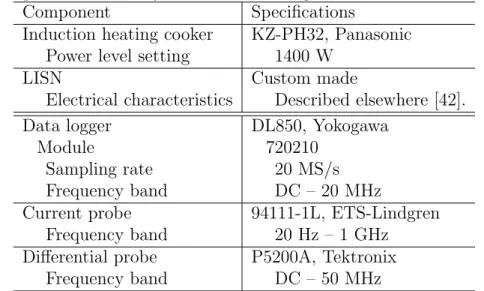
Table 2.2 Specifications of System for Measuring Conducted Disturbance Voltages.
Component Specifications
Induction heating cooker KZ-PH32, Panasonic Power level setting 1400 W
LISN Custom made
Electrical characteristics Described elsewhere [42].
Data logger DL850, Yokogawa
Module 720210
Sampling rate 20 MS/s
Frequency band DC – 20 MHz
Current probe 94111-1L, ETS-Lindgren
Frequency band 20 Hz – 1 GHz
Differential probe P5200A, Tektronix
Frequency band DC – 50 MHz
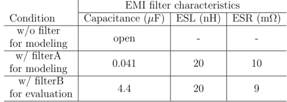
converter circuit. As the LISN, we used one prepared by our research group [42], which has impedance characteristics conformed to CISPR16-1-2 [43].
We applied the model shown in Fig. 2.2 to the whole circuit of the EUT, hence the model does not correspond exactly to the circuit configuration of the EUT. The model equivalently express the noise occurring in the EUT and its leakage.
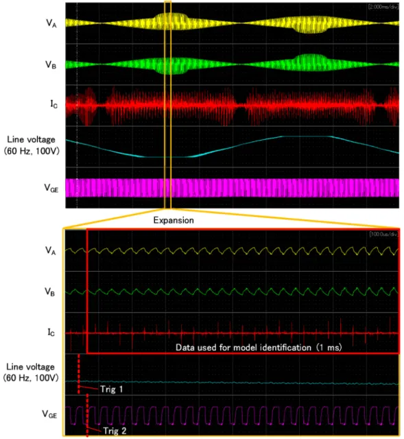
At the same time that we measured the voltage and current data ( ˙VL, ˙VN, ˙IL, ˙IN, and ˙IC) for use in identifying the model parameters, we also measured the gate-emitter voltage ˙VGE of an insulated-gate bipolar transistor (IGBT) mounted on the EUT PCB for use in aligning the phases of the data. We used a data logger (Yokogawa, DL850) to make the measurements. ˙VL, ˙VN, ˙IL, and ˙IN were measured indirectly; instead, they were calculated from the measured voltages at the LISN measurement ports ( ˙VA and ˙VB)
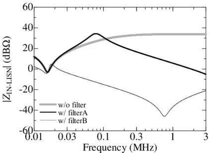
2.4 Parameter Identification 19 and the known LISN impedance [42]. The input impedance of the LISN looking from the EUT port ˙Zin is calculated by
Z˙in = ˙Z11− Z˙12 Z˙21
Z˙mp, (2.4)
where, ˙Zmp is the LISN measurement port impedance, ˙Z11, ˙Z12, ˙Z21, and ˙Z22 are Z- parameters of the LISN. ˙VL and ˙VN are calculated by
V˙L,N= Z˙in
Z˙21(1 + Z˙22
Z˙mp) ˙VA,B, (2.5)
I˙L and ˙IN are calculated by
I˙L,N= V˙L,N
Z˙in
. (2.6)
The data logger was connected to the LISN measurement ports by coaxial cables. The ports were terminated with 50-Ω resistors because the input impedance of the data logger was fixed at 1 MΩ. That is, ˙Zmpis 50-Ω. ˙IC was measured on the power cable between the LISN and EUT using a current probe (ETS-Lindgren, 94111-1L) and a 50-Ω termination resistor. ˙VGE was measured using a differential probe (Tektronix, P5200A). Besides, line voltage (60 Hz, 100 V) was measured using a coaxial cable as a trigger signal.
Fig. 2.5 shows time domain waveform of the conducted disturbances ( ˙VA, ˙VB, and ˙IC) and trigger signals ( ˙VGE and line voltage). ˙VA and ˙VB vary with the line voltage in top side of Fig. 2.5. ˙VA and ˙VB also vary with ˙VGE in bottom side of Fig. 2.5. Therefore, ˙VA and ˙VB should be obtained synchronized with both the line voltage and ˙VGE. ˙VA and ˙VB were obtained using two level triggers as shown in bottom side of Fig. 2.5. Besides, they were acquired at the sampling rate of 20 MHz during the period of 1 ms. Data used in the model identification ˙VL, ˙VN, ˙IL, and ˙IN were calculated by 2.5 and 2.6.
Fig. 2.6 shows the spectral envelopes of the measured voltage or current without the EMI filter. Since the fundamental switching frequency of the IGBT was 27 kHz, its harmonic components are plotted. Fig. 2.6(a) shows the conduction disturbance voltage, where ˙VL is shown as white circles, ˙VN is shown as black circles, and the noise floor is shown as a gray line. ˙VL and ˙VN were 10 dB or more greater than the noise floor up to 3 MHz, so we evaluated the proposed model in the frequency band up to 3 MHz. Fig. 2.6(b) shows the normal mode current, where ˙IL is shown as white circles, ˙IN is shown as black circles, and the noise floor is shown as a gray line. At the fundamental switching frequency having the highest current level, the magnitudes of the normal mode currents were 110 dBµA. When applying the method of Tarateeraseth et al. [12], in which the impedance characteristics are obtained by injecting the signal into a measurement system from a VNA, a current of 120 dBµA or more must be injected. This makes experimentation difficult because such large current is not available to output with commercial VNAs.
Figure 2.5 Time domain waveform of measured conducted disturbances and trigger signals.
2.4 Parameter Identification 21
(a)
(b)
(c)
Figure 2.6 Spectral envelopes of measured voltage or current without EMI filter: (a) V˙L and ˙VN, (b) ˙IL and ˙IN, and (c) ˙IC.