CRD-22AD12N
22kW Three Phase Bi-directional AFE ACDC CONVERTER
CRD-22AD12N
22kW 三相交流-直流双向变换器
CRD-22AD12N
22kW 三相交流-直流双向変換器
CRD-22AD12N User Guide
PRD-02282 Rev 0
Cree Power Applications
Cree, Inc. 4600 Silicon Drive Durham, NC 27703, USA 科税有限责任公司 4600 Silicon Drive Durham, NC 27703, USA クリー株式会社 4600 Silicon Drive Durham, NC 27703, USACREE® C3MTM SiC MOSFET
C3M0032120K TO-247-4 Package
This document is prepared as an application note to install and operate Cree® evaluation hardware.
All parts of this application note are provided in English, and the cautions are provided in English, Mandarin, and Japanese. If the end user of this board is not fluent in any of these languages, it is your responsibility to ensure that they understand the terms and conditions described in this document, including without limitation the hazards of and safe operating conditions for this board.
本文件中的所有内容均以英文书写,“注意”部分的内容以英文、中文和日语书写。作为本板 子的终端用户,即使您不熟悉上述任何一种语言,您也应当确保正确理解本文件中的条款与条 件,包括且不限于本板子的危险隐患以及安全操作条款。 当書類のすべての内容は英語で書きます。「注意点」の内容は英語、中国語、また日本語で 書きます。当ボードの端末使用者は上記の言語が一つでもわからないなら、当端末使用者は 当書類の条約と条件が理解できるのを確保すべきです。そして、当ボードの危険や安全に使 用する条件を含み、また限りません。
Note: This Cree-designed evaluation hardware for Cree® components is a fragile, high voltage, high temperature power electronics system that is meant to be used as an evaluation tool in a lab setting and to be handled and operated by highly qualified technicians or engineers. When this hardware is not in use, it should be stored in an area that has a storage temperature ranging from -40° Celsius to 105° Celsius. If this hardware is transported, special care should be taken during transportation to avoid damaging the board or its fragile components and the board should be transported carefully in an electrostatic discharge (ESD) bag, or with ESD or shorting protection that is the same as, or similar to, the protection that is or would be used by Cree when shipping this hardware, to avoid any damage to electronic components. Please contact Cree at [email protected] if you have any questions about the protection of this hardware during transportation. The hardware does not contain any hazardous substances, is not designed to meet any industrial, technical, or safety standards or classifications, and is not a production-qualified assembly.
本样机(易碎、高压、高温电力电子系统)由科锐为评估其功率半导体产品而设计,用以作为 在实验室环境下由专业的技术人员或工程师处理和使用的评估工具。本样机不使用时,应存储 在-40oC~105oC温度范围的区域内;如需运输样机,运输过程中应该特别小心,避免损坏电路 板等易碎组件。如果您对此硬件在运输之中的保护有任何疑问,请联系[email protected]。 样机应放置在防静电包装袋内谨慎运输,避免损坏电子组件。本样机不含任何有害物质,但其 设计不符合任何工业、技术或安全标准或分类,也不是可用于生产的组件。 このクリーのコンポーネント用評価ハードウェアは壊れやすい高電圧の高温パワーエレクトロニク スシステムであり、ラボ環境での評価ツールとして使用され、優秀な技術者やエンジニアによって 処理され、操作されることを意図している。ハードウェアが使用されていない場合、保管温度が-40℃から105℃の範囲に保管してください。このハードウェアを輸送する場合は、輸送中にボードま
たはその壊れやすいコンポーネントに損傷を与えないよう特別な注意を払う必要がある。また電子 部品の損傷を避けるためにボードを静電気放電(ESD)袋に静置して慎重に輸送するべき。ハード ウエアの輸送中の保護について質問があれば、[email protected]に連絡してください。ハード ウェアには危険物質が含まれていないが、工業的、技術的、安全性の基準または分類に適合する ように設計されておらず、生産適格組立品でもない。 CAUTION
PLEASE CAREFULLY REVIEW THE FOLLOWING PAGES, AS THEY CONTAIN IMPORTANT INFORMATION REGARDING THE HAZARDS AND SAFE OPERATING REQUIREMENTS RELATED TO THE HANDLING AND USE OF THIS BOARD.
警告 请认真阅读以下内容,因为其中包含了处理和使用本板子有关的危险隐患和安全操作要 求方面的重要信息。 警告 ボードの使用、危険の対応、そして安全に操作する要求などの大切な情報を含むの で、以下の内容をよく読んでください。
CAUTION
DO NOT TOUCH THE BOARD WHEN IT IS ENERGIZED AND ALLOW THE BULK CAPACITORS TO COMPLETELY DISCHARGE PRIOR TO HANDLING THE BOARD. THERE CAN BE VERY HIGH VOLTAGES PRESENT ON THIS EVALUATION BOARD WHEN CONNECTED TO AN ELECTRICAL SOURCE, AND SOME COMPONENTS ON THIS BOARD CAN REACH TEMPERATURES ABOVE 50˚ CELSIUS. FURTHER, THESE CONDITIONS WILL CONTINUE FOR A SHORT TIME AFTER THE ELECTRICAL SOURCE IS DISCONNECTED UNTIL THE BULK CAPACITORS ARE FULLY DISCHARGED.
Please ensure that appropriate safety procedures are followed when operating this board, as any of the following can occur if you handle or use this board without following proper safety precautions:
● Death
● Serious injury ● Electrocution ● Electrical shock ● Electrical burns ● Severe heat burns
You must read this document in its entirety before operating this board. It is not necessary for you to touch the board while it is energized. All test and measurement probes or attachments must be attached before the board is energized. You must never leave this board unattended or handle it when energized, and you must always ensure that all bulk capacitors have completely discharged prior to handling the board. Do not change the devices to be tested until the board is disconnected from the electrical source and the bulk capacitors have fully discharged.
警告 请勿在通电情况下接触板子,在操作板子前应使大容量电容器的电荷完全释放。接通 电源后,该评估板上通常会存在危险的高电压,板子上一些组件的温度可能超过 50 摄 氏度。此外,移除电源后,上述情况可能会短时持续,直至大容量电容器电量完全释 放。 操作板子时应确保遵守正确的安全规程,否则可能会出现下列危险: ● 死亡 ● 严重伤害 ● 触电 ● 电击 ● 电灼伤 ● 严重的热烧伤 请在操作本板子前完整阅读本文件。通电时禁止接触板子。所有测试与测量探针或附 件必须在板子通电前连接。通电时,禁止使板子处于无人看护状态,且禁止操作板子。 必须确保在操作板子前,大容量电容器已释放了所有电量。只有在切断板子电源,且 大容量电容器完全放电后,才可更换待测试器件。
警告 通電している時、ボードに接触するのは禁止です。ボードを処分する前に、大容量のコンデ ンサーで電力を完全に釈放すべきです。通電してから、ボードにひどく高い電圧が存在して いる可能性があります。ボードのモジュールの温度は 50 度以上になるかもしれません。ま た、電源を切った後、上記の状況がしばらく持続する可能性がありますので、大容量のコン デンサーで電力を完全に釈放するまで待ってください。 ボードを操作するとき、正確な安全ルールを守るのを確保すべきです。さもないと、以下の 危険がある可能性があります: ● 死亡 ● 重症 ● 感電 ● 電撃 ● 電気の火傷 ● 厳しい火傷 当ボードを操作する前に、完全に当書類をよく読んでください。通電している時にボードに 接触する必要がありません。通電する前に必ずすべての試験用のプローブあるいはアクセサ リーをつないでください。通電している時に無人監視やボードを操作するのは禁止です。ボ ードを操作する前に、大容量のコンデンサーで電力を完全に釈放するのを必ず確保してくだ さい。ボードの電源を切った後、また大容量のコンデンサーで電力を完全に釈放した後、試 験設備を取り換えることができます。
Table of Contents
... 7 ... 8 ... 10 ... 13 ... 20 ... 26This User’s Guide provides the schematic, artwork, and test setup necessary to evaluate Cree’s CRD-22AD12N, 22KW Bi-Directional Active Front End(AFE) converter for an electric vehicle (EV) on-board charger (OBC) and similar applications.
A block diagram of 22kW OBC based on SiC is shown in Figure 1. This design of Cree’s 22KW, Bi-Directional AFE converter (P/N CRD-22AD12N) is based upon one of Cree’s latest generation of SiC MOSFETs - C3M0032120K (1200V, 32mΩ, TO-247-4). This reference design is the grid connected stage of a bi-directional OBC converter. As shown in Figure 1, it operates from grid supply at AC terminals and provides a non-isolated DC output voltage at the DC terminals (referred to as rectifier mode) or vice versa (referred to as inverter mode). Please refer to Cree’s 22kW isolated DC/DC converter (P/N CRD-22DD12N) for the DC/DC stage.
Figure 1. Block Diagram of Cree’s CRD-22DD12N and CRD-22AD12N, 22KW Bi-Directional EV On-board charger
The classic AFE topology using a six-switch, two-level converter, is chosen to meet high efficiency, high power density and bi-directional operation requirements. The converter operates at a fixed 45kHz switching frequency for both charging and discharging modes. An extruded heatsink and fan are used to cool the MOSFETs to simplify bench testing in place of a cooling plate in an OBC application.
In charging mode, the DC output voltage is adjustable between 650Vdc and 900Vdc for three-phase AC input or between 380Vdc and 900Vdc for a single-three-phase AC input. This variable bus voltage helps to realize a wide output voltage range for the DC/DC stage. In an OBC application, a phase AC output is required in discharging mode, therefore, a single-phase inverter is demonstrated.
Since the main purpose of the reference design is to demonstrate the performance of SiC in the power converter for OBC applications, only standalone load is supported. Thus, this reference design doesn’t focus on techniques related to a grid-connected inverter and there is no grid-connected inverter algorithm built in. A resistive load connected to the single-phase AC output is recommended when operating in inverter mode. An electronic load or a resistive load may be used on the DC output when operating in rectifier mode.
This reference design board uses Cree’s C3M0032120K, 1200V, 32mΩ, SiC MOSFETs (TO-247-4). A single SiC MOSFET is used for each position.
This AFE evaluation board is compatible for both single-phase and three-phase application. In inverter mode, the three-phase application is only used for gate driver signal verification, not for power test. Thus, the power direction and converter configuration should be selected properly via the graphical user interface (GUI) before turning on the unit.
The operational range of the evaluation board in charging mode is as shown in Table 1. The output power should not exceed 22kW for three-phase application and 6.6kW for single-phase application. The Root Mean Square (RMS) value of the input line current should not exceed 32A in any condition.
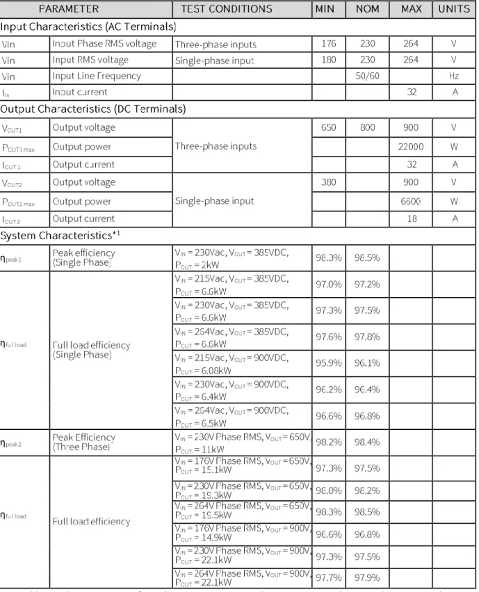
Operation Mode Input AC RMS Range Input Line Current Output DC Range Output Power three-phase charging 176Vphase ~ 264Vphase 32A RMS Max. 650VDC~900VDC 22kW Max.
single-phase charging 180V AC ~ 264V AC 380VDC~900VDC 6.6kW Max.
Table 1: Overall Charging Operation
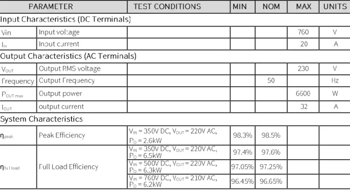
Operation Mode Max. Input DC Max. Output AC RMS Max. Output Power single-phase inverter mode 760V DC 220V RMS 6.6kW
Table 2: Overall Discharging Operation (Open Loop)
The hardware can support 480VAC three-phase input, but the software is not designed to be compatible for it.
A user should not overload the converter out of the SOA (Safe Operation Area). Please refer to Table 7 in Section 6.3 of this User’s Guide for protection details.
A GUI communicates to the unit via a controller area network (CAN) communication bus. It is used to display operational information and provide related user controls, such as the selection of power direction and topology. The output voltage is configurable through the CAN interface in rectifier mode. The output voltage is fixed at about 220V RMS max for a single-phase inverter operation. No load is allowed for three-phase application in inverter mode.
2
ƞ
η
ƞ
η
Table 3: Characteristics of Cree’s CRD-22AD12N, 22 kW Bi-Directional AFE in Charging Modes *1: Maximum current is about 30A for the efficiency test due to the limitation of the power analyzer. Output power is not exactly the same as target at high voltage because resistive load is used.
ƞ
η
Table 4: Characteristics of Cree’s CRD22AD12N, 22 kW Bi-Directional AFE in Single-phase Discharging Mode
The primary application for Cree’s CRD-22AD12N reference design board is isolated Bi-Directional EV charging systems, but the output must be connected to a resistive load or electronic load (CR (Constant Resistor) mode recommended). A battery test is not allowed since a battery-charging algorithm has not been implemented in the design.
Some of the features and limitations of Cree’s CRD-22AD12N reference design board are listed below:
• Bi-directional operation:DC output range is 380Vdc-900Vdc for single-phase and 650Vdc-900Vdcfor three-phase inputs.
• Maximum allowed AC line current is 32A and maximum affordable output DC power is 22kW. Only rectifier mode is allowed for three-phase application. • Maximum output power is 6.6kW for single-phase application.
• Peak efficiency > 98.3%.
• Protection functions are shown in Table 7.
• Easy to test using a GUI communicating via CAN. See Section 5 and Section 12 for details.
Note: A larger copy of any diagram in Section 4 may be downloaded from the Wolfspeed® reference design website ( https://www.wolfspeed.com/power/products/reference-designs/) or obtained upon request by contacting Cree at .
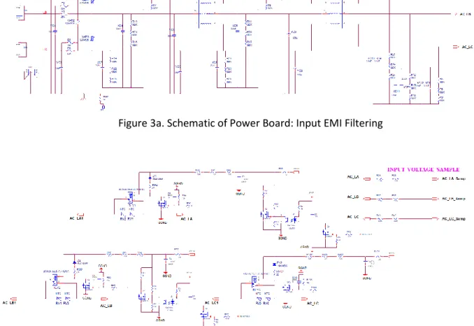
Schematics of the power, control, and auxiliary-power boards are shown in Figures 3 through 10.
Figure 3a. Schematic of Power Board: Input EMI Filtering
Figure 3c. Schematic of Power Board: Main Inverter MOSFETs and DC Bus
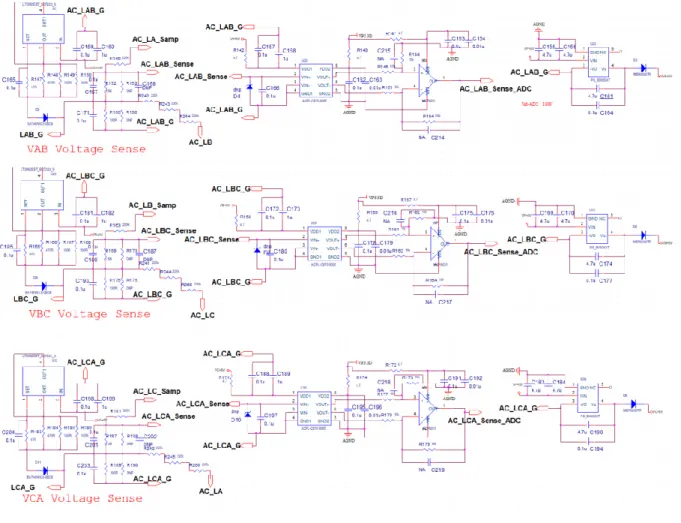
Figure 3d. Schematic of Power Board: Current Sensing
Figure 4b. Schematic of Power Board: Linear Regulators and Isolated Gate Power Supplies
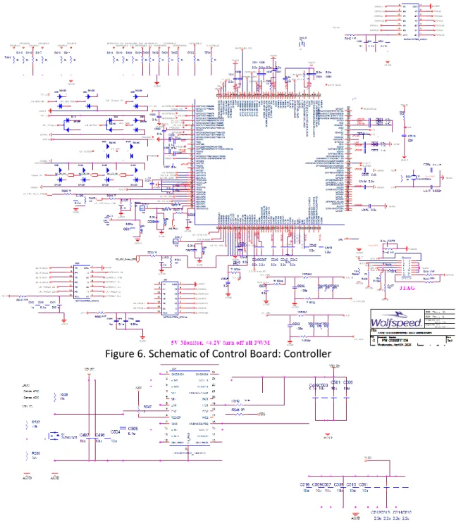
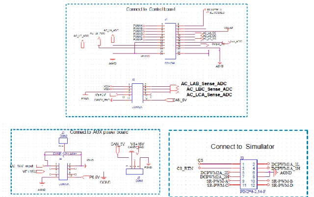
Figure 6. Schematic of Control Board: Controller
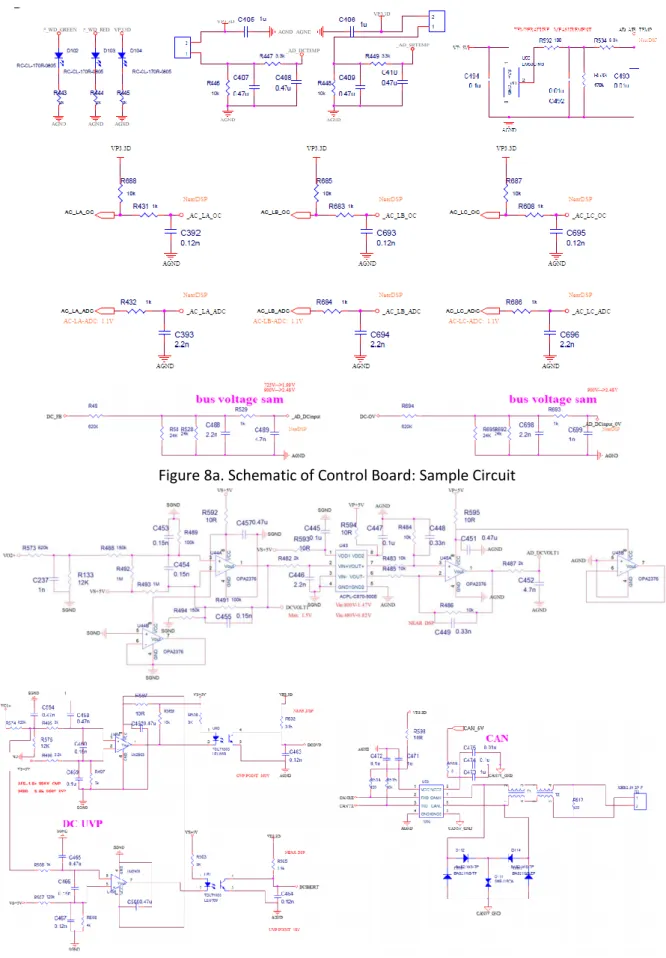
Figure 8a. Schematic of Control Board: Sample Circuit
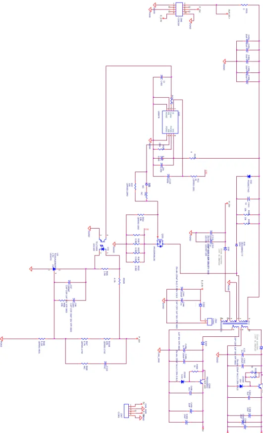
Figure 9. Schematic of Auxiliary Power Board C 451 10uF C 452 10uF C 453 10uF J 344 C ON 2 1 2 R 535 0 R 531 0 ISGN D ISGN D AU X _D C + C 4501n Q331 IPD 220N 06L3G R 536 1k R 537 1k C 454 10uF C 455 10uF ISGN D Title Size Document Number Rev Date: Sheet of xxx A 6. 6k W Bi-direc tion OBC f or EV c harger - Aux Prim ary C 7 9 Sat urday , Sept em ber 29, 2018 + C 309 10uF Q302 PBSS306N Z SOT -223 D 39 STPS3150UF DIODE SCHOTTKY 150V 3A SMAFLAT R 538 10k Z D 300 15V R 539 10k C 310 0u1 C 111 1u D 32 F 6165C T -N D D 25 1N 4148W Q-7-F 100V C 22 1u C AP C ER 1U F 50V X 7R 0603 C 313 1u LEC 007-105 C AP C ER 0. 1U F 25V X 7R 0603 D 35 NC D 30 S_15V SGN D R 532 0. 082 PGN D P_15V PGN D R 1 0 8 22k LER 001-1742 R 4 8 5 .1 K LER 001-4531 C 116 NC R 4 7 2 .7 k LER 001-1742 R 4 6 NC P_15V PGN D + C 445 10uF T 12 C R 6600F Z 1 2 10 4 5 9 1 3 6 8 7 C 95 100n C AP C ER 33nF 50V X 7R 0603 C 67 1000pF C AP C ER 1nF 50V X 7R 0603 R 5 6 10k U 11 T C LT 1003 LEU 169 1 2 4 3 R 4 5 1 .5 k U9 T L431AQD BZ R LEU 072 1% 2. 5V 1 2 3 R 5 2 6 4 .7 k C 45610u D _6. 5V D GN D P_15V PGN D R 11 1k LER 001-1001 R 38 0. 082 R 52 NC R 39 0. 082 R 37 100 LER 003-10R 0 C 118 100p R 5 4 10k LER 001-1002 ISGN D C S1 R 527 0. 082 CS1 + C 442 10uF + C 443 10uF J 346 C ON 10A 1 2 3 4 5 6 7 8 9 10 + C 435 10uF Q330 PBSS306N Z SOT -223 S_15V ES1B 100V 1A R 409 1k SGN D Z D 326 5. 6V LM 3478 IS U22 1 C om p 2 FB 3 AGN D 4 PGN D 5 DR 6 F A/ SD 7 VI N 8 C 436 0u1 C 438 1u 1U F 50V X 7R 0603 D 329 5V 5V C AN _GN D C 312 220uF 25v olt s 220uF 8x 11. 5 20% 3. 5LS C 113 220uF LEC 231 25v olt s 220uF 8x 11. 5 20% 3. 5LS C 439 220uF 25v olt s 220uF 8x 11. 5 20% 3. 5LS J 347 C ON 5 1 2 3 4 5 ES2BA-13-F 100V 2A C 440 1u C AP C ER 1U F 50V X 7R 0603 D 330 C 441 220uF 25v olt s 220uF 8x 11. 5 20% 3. 5LS C AN _GN D SGN D R 528 150k D GN D STPS3150UF DIODE SCHOTTKY 150V 3A SMBFLAT C 448 0.1u D _6. 5V R 530 1k ISGN D
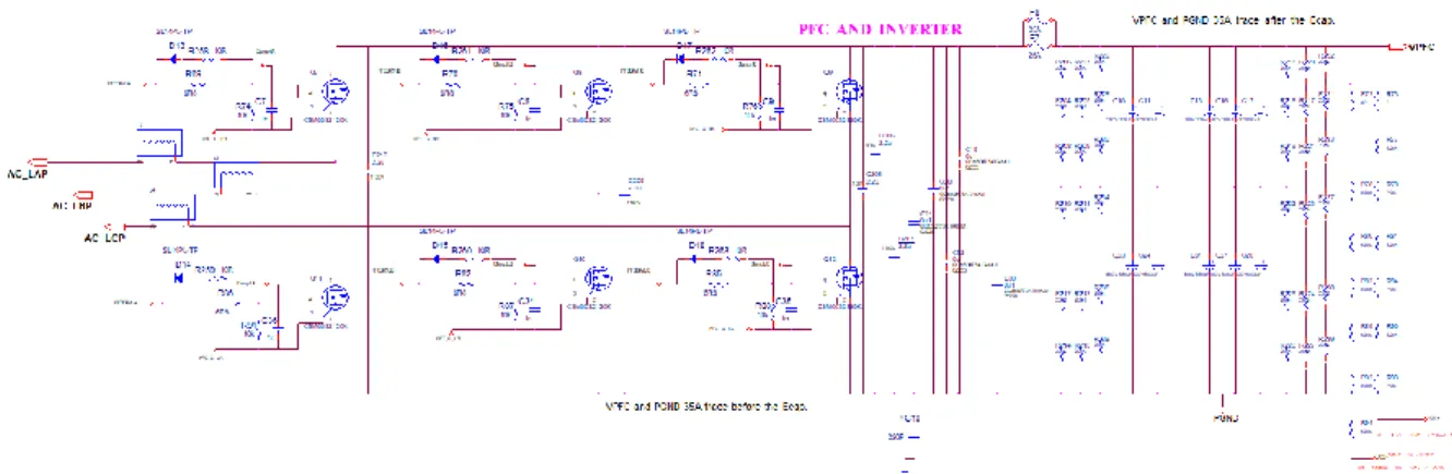
As illustrated by Figure 3a to 3d, a six-switch, two-level topology is selected for the converter. Three-phase AC line supply in positive sequence is connected to terminals “A,” “B,” and “C” of CON1, 2, and 3 respectively, followed by three-phase fuses (F1~F6) and MOVs (VAR1~VAR3). Electro-magnetic interference (EMI) filters CL1_A1 and CL2_A1 and X/Y capacitors are connected next. This is followed by relays (RLY1, RLY2 and RLY3) and Negative temperature coefficient (NTC) resistors (RV1~RV6) through which the DC link capacitors are charged. NTC resistors will be short-circuited by relays when the DC link voltage is charged. Three Power factor correction (PFC) chokes are connected between relays and midpoints of a three-phase bridge consisting of CREE SiC MOSFETs (Q7~Q12). The bus-side DC terminals are CON5(+) and CON6(-), followed by ten electrolytic capacitors (five parallel sets of two in a series) which absorb the high-frequency ripple on the DC port. Several film and ceramic capacitors are also arranged in parallel.
For compatible single-phase application, terminals “B” and “C” are used as inputs for L and N. In this situation, relay in phase “A” is always open and terminal “A” should remain unconnected.
As illustrated by Figures 4a to 4b, all Texas Instruments Inc. gate drivers (P/N: UCC5350MCQDQ1) are separately powered by isolated, DC/DC power supplies with VIN = +15V and VOUT = +15V/-3V from RECOM Power GmbH. (P/N: R15P21503D). Input voltage sensing circuits are illustrated in Figure 5.
As illustrated by Figure 6 to 8, the control board, which carries out the control algorithm of the entire system, is designed around a Texas Instruments Inc. controller (P/N: TMS320F28377D). The power supply for the control board is an isolated, 7V@1A power supply whose output is then tightly regulated to +5.0V by a linear regulator. This 5.0V voltage rail then supplies another precision linear regulator, U57, from Texas Instruments Inc. (P/N: TPS70445), which provides both a 3.3V and a 1.2V voltage rail. All output drive signals are buffered and shifted to a +5V level by a Fairchild Semiconductor International Inc. level-shifter (P/N: MC74HCT50A). The reference voltage for the controller’s ADC (Analog-to-Digital Converter) is 3.3V. This reference voltage is created by a reference IC U9, (P/N: AZ431-2.5V) from the +5.0V rail.
The reference ground of the control board is the negative terminal of the DC bus. The voltage sample signal and OVP/UVP (Over/Under Voltage Protection) signals of the DC bus are isolated by optocouplers before they are fed into the controller for further processing.
The typical input voltage of the auxiliary power board is 14V (J6-2 = +14V, J6-1=14V Return). It provides four isolated output voltages, as shown in Table 5.
Table 5: Input and Outputs of Auxiliary Power Board
AC Input Source: The input source must be an adjustable AC source whose output can be adjusted between 90Vac and 300Vac. It must be capable of supplying at least 25000W.
Output Load: A programmable high-voltage electronic load or a high-voltage resistor bank may be used. Each must be capable of sinking 36A of load current supplied from the evaluation board whose output can be 1000Vdc/22kw.
Power Meter: A power analyzer from Yokogawa Test and Measurement Corporation (P/N: WT 3000) or any other equivalent power analyzer should be used. An external shunt resistor should be used when the output current exceeds the rating of the internal shunt resistor.
Oscilloscope: A 300MHz or greater digital or analog oscilloscope with 100MHz or greater isolated differential voltage probes and isolated current probes (i.e., Hall effect) should be used.
Power Supplies: The following power supplies with isolated grounds should be used and must be obtained separately:
1) 14V @ 1.5A capability is required to supply the auxiliary power board. 2) 12VDC @ 12A capability in total is required to power the cooling fans.
External Fans: Cooling fans should be used and must be obtained separately. As shown in Figure 11, at least two cooling fans, such as the Delta Electronics Inc. DC12V/3.30A fan (P/N: PFR0612XHE) or an equivalent fan, must be used for cooling the baseplate. Another fan is used to cool the magnetics. The fans can be placed to let the air flow go to the three PFC inductors and the CM inductors. The red wire of the fan is the positive terminal and the black wire is the negative terminal. The temperature of the magnetics should be monitored by an infrared scanner to verify the cooling fan setup during first-time testing.
Figure 11. Setup of the Reference Design
Recommended Wire Gauge: Cable with a minimum AWG #10 wire gauge is recommended to carry the DC input and output currents.
A Windows C# GUI in conjunction with USB-CAN tools (GCAN: USBCAN-I) is provided for testing. Connector J11 is used for CAN, as shown in Figure 11.
The over/under voltage-protection is indicated by the back color of the voltage value, as shown in Figure 12a to Figure12e. “Green” indicates “Normal Operation” while “Red” indicates “Warning Issued.” The ambient temperature sensed by the IC is displayed in the panel as well.
Figure 12a. CAN Status Tab after Connection Figure 12b. Connected to Control Board <Off Mode>
The power direction and topology can only be changed when the rectifier is shut down. This can be accomplished in two steps: first send an “OFF” command to shut down the converter, then send an “ON” command with correct power direction and topology. The converter will shut down and ignore any other configuration bits once it receives the CAN frame with the “OFF” configuration. If the converter is shut down, it will start as configured once it receives the CAN frame with the “ON” configuration. The current power direction and topology will also display in the left bottom area.
Voltage reference is the desired output DC voltage in charging mode. The digital controller will check the value range each time. In discharging mode, these reference values have no impact.
Figure 12e. Discharging Operation in Single Phase
OVP fault will be generated if a user connects three-phase power when the software is configured for single phase. To correct this issue, turn the unit off and change the setting to match the correct input.
The reference design communicates over a CAN V2.0B bus at 250K bps (bits per second) using extended frame format (29 bits extend ID). The data length is 8 bytes in big endian format. All registered CAN messages are listed in Section 12.2 and 12.3.
Table 6 below provides an example when “0x18A5E5F4” is sent as the message identifier and “0x0100FFFF19640168” is sent as the CAN data. When the OBC is placed in charging mode, its output voltage is set to 650V and care must be taken to ensure that the first byte in the CAN instruction matches the correct operating mode when the second byte is zero. Otherwise, that instruction will be ignored by the reference board.
There is no current limit function for AFE, so the current reference has no impact at all. User should take precautions to prevent overloading.
01 00
1964 0168
1964 0168
CAUTION
IT IS NOT NECESSARY FOR YOU TO TOUCH THE BOARD WHILE IT IS ENERGIZED. WHEN DEVICES ARE BEING ATTACHED FOR TESTING, THE BOARD MUST BE DISCONNECTED FROM THE ELECTRICAL SOURCE AND ALL BULK CAPACITORS MUCH BE FULLY DISCHARGED.
SOME COMPONENTS ON THE BOARD REACH TEMPERATURES ABOVE 50⁰ CELSIUS. THESE CONDITIONS WILL CONTINUE AFTER THE ELECTRICAL SOURCE IS DISCONNECTED UNTIL THE BULK CAPACITORS ARE FULLY DISCHARGED. DO NOT TOUCH THE BOARD WHEN IT IS ENERGIZED AND ALLOW THE BULK CAPACITORS TO COMPLETELY DISCHARGE PRIOR TO HANDLING THE BOARD. PLEASE ENSURE THAT APPROPRIATE SAFETY PROCEDURES ARE FOLLOWED WHEN OPERATING THIS BOARD AS SERIOUS INJURY, INCLUDING DEATH BY ELECTROCUTION OR SERIOUS INJURY BY ELECTRICAL SHOCK OR ELECTRICAL BURNS, CAN OCCUR IF YOU DO NOT FOLLOW PROPER SAFETY PRECAUTIONS.
警告 通电时不必接触板子。连接器件进行测试时,必须切断板子电源,且大容量电 容器必须释放完所有电荷。 板子上一些组件的温度可能超过 50 摄氏度。移除电源后,上述情况可能会短暂 持续,直至大容量电容器完全释放电荷。通电时禁止触摸板子,应在大容量电 容器完全释放电荷后,再操作电路板。 请确保在操作电路板时已经遵守了正确的安全规程,否则可能会造成严重伤 害,包括触电死亡、电击伤害、或电灼伤。 警告 通電している時にボードに接触する必要がありません。設備をつないで試験 する時、必ずボードの電源を切ってください。また、大容量のコンデンサー で電力を完全に釈放してください。 ボードのモジュールの温度は 50 度以上になるかもしれません。電源を切った 後、上記の状況がしばらく持続する可能性がありますので、大容量のコンデ ンサーで電力を完全に釈放するまで待ってください。通電している時にボー ドに接触するのは禁止です。大容量のコンデンサーで電力をまだ完全に釈放 していない時、ボードを操作しないでください。 ボードを操作している時、正確な安全ルールを守っているのを確保してくだ さい。さもなければ、感電、電撃、厳しい火傷などの死傷が出る可能性があ ります。
Figure 13. Converter Test Setup
Miniature circuit breaker (MCB) is optional for the testing setup. Charging mode includes the three-phase AC/DC operation and single-phase AC/DC operation using AC terminal “B” and “C”.
• Connect resistive load to the DC port of the evaluation board.
• Connect AC source to the AC terminals of the evaluation board. AC terminal “A” should be kept floating for single-phase operation.
• Connect power analyzer to measure input and output power.
• Use appropriately rated voltage and current probes and connect to the oscilloscope. • Place and operate the external fans.
Figure 14. Converter Test Setup
MCB1 and MCB2 are optional for the testing setup. Discharging mode refers to single-phase DC/AC operation only using AC terminals “B” and “C.” Three-phase inverter mode is only used for three-phase drive check.
• Connect resistive load to the AC terminals “B” and “C” of the evaluation board. • Connect DC source to the DC port of the evaluation board.
• Connect power analyzer to measure input and output power.
• Use appropriately rated voltage and current probes and connect to the oscilloscope. • Place and operate the external fans.
Table 7 describes over/under voltage protection (OVP/UVP) and over current protection (OCP) functions in the reference design.
Do not overload the converter outside the operating specs.
The requirements for the isolated power supply are shown in Table 8. A single power supply connected to J6 is used to power the on-board auxiliary power board. The cooling fans (DC12V/3.30A) are independently powered.
ingle
Table 8: Auxiliary Power Supply Requirements
All power MOSFET pins are exposed. Their gate and drain voltages must be measured with caution. Probes should be connected to them only after the removal of input power and only after all bulk capacitors have fully discharged.
警告 ***高压危险*** 通电后,评估板上会存在危险的高电压,且板子上一些组件的温度会超过 50 摄氏度。 断电后,上述情况可能会持续存在,尤其是大容量电容器可能会残存危险的高电压。 通电时禁止对板子进行任何操作。操作板子前,请确保大容量电容器电量已完全释放。 板子上的连接器在通电时存在危险的高电压。即使已断电情况下,在大容量电容电量 完全释放前,其连接器仍可能存在危险的高电压。请确保在正确的安全流程下进行操 作,否则可能会造成严重伤害,包括触电死亡、电击伤害或电灼伤。操作板子前,请 务必切断供电电源,并且确认大容量电容器电量已完全释放。使用后应立即切断板子 电源。切断电源后,其连接器由于大容量电容存在而仍可能有危险的高电压。因此, 在接触板子前,除断电外还需要确保大容量电容器电量已完全释放。 警告 ***高圧危険*** 通電してから、ボードにひどく高い電圧が存在している可能性があります。ボードのモジ ュールの温度は 50 度以上になるかもしれません。また、電源を切った後、上記の状況がし ばらく持続する可能性がありますので、大容量のコンデンサーで電力を完全に釈放するま で待ってください。通電している時にボードに接触するのは禁止です。 大容量のコンデンサーで電力をまだ完全に釈放していない時、ボードに接触しないでくださ い。ボードのコネクターは充電中また充電した後、ひどく高い電圧が存在しているので、大 容量のコンデンサーで電力を完全に釈放するまで待ってください。ボードを操作している時、 正確な安全ルールを守っているのを確保してください。さもなければ、感電、電撃、厳しい 火傷などの死傷が出る可能性があります。設備をつないで試験する時、必ずボードの電源を 切ってください。また、大容量のコンデンサーで電力を完全に釈放してください。使用後、 すぐにボードの電源を切ってください。電源を切った後、大容量のコンデンサーに貯蓄して いる電量はコネクターに持続的に入るので、ボードを操作する前に、必ず大容量のコンデン サーの電力を完全に釈放するのを確保してください。
Notes:
1. Power direction (rectifier mode or inverter mode) and topology (single-phase or three-phase) cannot be changed after start-up.
2. Choose the appropriate power direction and topology matched with the setup. Phase AC terminal “A” should be left floating if the converter operates as single-phase rectifier or inverter.
3. Do not overload the converter. The AC line RMS current should not exceed 32A and the DC output power should not exceed 6.6kW for single-phase rectifier and 22kW for three-phase rectifier.
4. There is no current inrush limiter for DC port. The DC input voltage must be increased slowly (soft-start) for inverter mode.
5. Always remember to connect the cooling fans to their power supplies and operate the cooling fans when operating the board.
Please take the following steps in order when starting the unit in this mode:
1. Double check the setup: Make sure the polarity is correct, the DC source is connected to the DC terminals, and the load is connected to the AC terminals “B” and “C” (terminal “A” unconnected).
2. DC source output disabled.
3. Ensure that the load is less than 1KW.
4. Apply 14Vdc to J6 on the power board. Check the output voltage of the Auxiliary Power Supply at J7 (P6.5V, VP+15V) and J8 (VS+15V, CAN_5V). Check that the current draw is approximately the same as shown in Table 9. Check the +3.3V LED (on) and watchdog LED (blinking) on the control board.
5. Connect the GUI to the system. Send “OFF” command after it is connected successfully.
6. Apply power to the cooling fans.
7. Turn on the DC supply and increase it slowly from 0V to the required voltage (380Vdc – 760Vdc).
8. Verify that the measured values in the GUI are reported correctly.
9. Send ON command with settings of “Inverter” and “Single Phase.” Voltage reference has no impact for inverter mode.
10. After the output voltage has reached steady-state regulation, increase the load up to desired value with a maximum of 6.6kW. The step-load change should not be larger
than 1KW for each step.
11. Check the efficiency under load conditions of interest.
1. Decrease the load to 1KW in less than 1KW steps. 2. Use GUI to send OFF command.
3. Disable the output of the DC power supply.
4. Wait until the DC source has fully discharged its output.
5. Turn OFF load after the bus-side capacitors are fully discharged.
6. Capacitors may remain charged for up to 30 minutes after the circuit is turned OFF if step 4 or step 5 are skipped or compromised. They must be allowed to fully discharge before handling the board. Please check the terminal voltages with a multimeter to ensure that the board has fully discharged and is therefore safe to handle.
7. Turn OFF the 14Vdc power supply on J6. The unit should be fully discharged before the auxiliary power supply is disabled.
Please take the following steps in order when starting the unit in this mode:
1. Double check the setup: Make sure the AC source is connected to the AC terminals, and the load is connected to the DC terminals. For single-phase operation the AC source should be connected to terminals “B” and “C.” Terminal “A” should be left floating.
2. Check the input status and make sure the AC source output is disabled. 3. Make sure no load is applied to the DC terminals until step 11.
4. Apply 14Vdc to J6 on the power board. Check the output voltage of the Auxiliary Power Supply at J7 (P6.5V, VP+15V) and J8 (VS+15V, CAN_5V). Check that the current draw is approximately the same as shown in Table 9. Check the +3.3V LED (on) and watchdog LED (blinking) on the control board.
successfully.
6. Apply power to the cooling fans.
7. Turn on the AC supply (215V~264V RMS line-to-neutral).
8. Verify that the measured values in the GUI were reported correctly.
9. Send ON command with settings of “Rectifier” and “Three Phase” or “Single Phase,” according to desired output voltage. The converter will start up with the voltage according to Table 1.
10. The output voltage can be regulated using the GUI.
11. After the output voltage has reached steady-state regulation, apply a load to the output in no more than 2KW steps. Permanent overload damage may occur during sustained operation with unmatched input and output.
12. Check the efficiency under load conditions of interest.
1. Decrease the load to 1KW. Do not remove all load or the output capacitors will remain charged for at least 30 minutes after power down. The step of load change should be less than 2KW for each step.
2. Use GUI to send OFF command.
3. Turn OFF the AC source.
4. Wait until the AC source has fully discharged its output.
5. Turn OFF load after the battery side capacitors are fully discharged.
6. Capacitors may remain charged for up to 30 minutes after the circuit is turned OFF if steps 1, 4, or 5 are skipped or compromised. They must be allowed to fully discharge before handling the board. Please check the terminal voltages with a multimeter to ensure that the board has fully discharged and is therefore safe to handle.
Figure 15 shows the locations of the terminals, key components, and daughter-boards on the Power Board.
Figure 15. Top View of PCBA (430mm*180mm*150mm)
Output Capacitance C3M0032120K PFC Inductors Cooling Fans
The performance data of Cree’s CRD-22AD12N reference design board is taken in AC/DC single-phase and three-phase charging modes, and DC/AC single-phase discharging. Table 10 to Table 17 indicates the performance data.
Input Voltage (Vac) Input Power (W) Load (%) Output Voltage (Vdc) Output Power (W) Overall Efficiency (%) 230 680.97 10 385 663.1 97.376 230 1348.2 20 385 1328.6 98.547 230 2025.6 30 385 1999.2 98.698 230 2701 40 385 2665.5 98.684 230 3332.2 50 385 3286.3 98.622 230 4011.9 60 385 3950.2 98.462 230 4697.1 70 385 4616.4 98.281 230 5300.1 80 385 5201.8 98.144 230 6062.1 90 385 5936.8 97.933 230 6597.2 100 385 6450.5 97.776 230 683.97 10 650 648.23 94.774 230 1332.8 20 650 1292 96.939 230 1986.6 30 650 1938.7 97.591 230 2710 40 650 2650.9 97.818 230 3368.3 50 650 3295.3 97.833 230 4030.7 60 650 3943.2 97.829 230 4662.5 70 650 4556.4 97.724 230 5331.2 80 650 5203.1 97.597 230 6007.3 90 650 5853.8 97.445 230 6691.3 100 650 6509.1 97.274 230 869.88 10 900 801.5 92.14 230 1275.4 20 900 1203 94.326 230 2084 30 900 2000.6 95.997 230 2487 40 900 2397.5 96.401 230 3301.7 50 900 3195.2 96.775 230 4125.1 60 900 3996.1 96.869 230 4895.7 70 900 4742.5 96.876 230 5313.7 80 900 5145.9 96.84 230 6149.6 90 900 5948.3 96.723 230 6585.3 100 900 6365.9 96.668
Figure 16: Efficiency Data (AC/DC Single-Phase Mode), VIN = 230Vac Input Voltage (Vac) Input Power (W) Load (%) Output Voltage (Vdc) Output Power (W) Overall Efficiency (%) 180 682.31 10 385 660.6 96.807 180 1338.24 20 385 1311.9 98.033 180 2017.3 30 385 1978.5 98.078 180 2732 40 385 2675.4 97.931 180 3346.6 50 385 3270.1 97.712 180 4063.8 60 385 3932.6 97.424 180 4710.8 70 385 4574.6 97.109 180 5175 80 385 5013.5 96.88 180 676.97 10 650 637.1 94.099 180 1309.87 20 650 1262.3 96.361 180 2143.6 30 650 2079.5 97.01 180 2576.1 40 650 2500.3 97.056 180 3445.4 50 650 3340.1 96.944 180 4104.9 60 650 3971.7 96.756 180 4569.3 70 650 4414.1 96.606 180 5236.7 80 650 5045.3 96.345 180 875.26 10 900 808.4 92.345 180 1286.56 20 900 1214.1 94.36 180 2103.8 30 900 2013.4 95.7 180 2511.44 40 900 2489.9 95.957 180 3341.85 50 900 3213.7 96.166 180 4205 60 900 4033.7 95.927 91 92 93 94 95 96 97 98 99 0 1000 2000 3000 4000 5000 6000 7000 Effi cien cy( %) Output Power (W)
AFE Efficiency under Single-Phase AC/DC Mode 230Vac
230Vac 380Vdc 230Vac 650Vdc 230Vac 900Vdc
180 5055 70 900 4841.4 95.776 180 5489 80 900 5254.5 95.728
Table 11: Efficiency Data (AC/DC Single-Phase Mode), VIN = 215Vac
Figure 17: Efficiency Data (AC/DC Single-Phase Mode), VIN = 215Vac
Input Voltage (Vac) Input Power (W) Load (%) Output Voltage (Vdc) Output Power (W) Overall Efficiency (%) 215 682.74 10 385 660.76 96.77 215 1346.3 20 385 1322.9 98.257 215 2020.7 30 385 1989.4 98.451 215 2693.4 40 385 2651.6 98.45 215 3369.1 50 385 3312 98.317 215 4042.3 60 385 3967.6 98.152 215 4675.6 70 385 4582.4 98.007 215 5361.3 80 385 5244.8 97.828 215 6049.1 90 385 5902.4 97.575 215 6202.1 100 385 6049.5 97.539 215 6.1561 10 650 1264.4 96.421 215 9.1546 20 650 1896.1 97.154 215 12.481 30 650 2590.7 97.447 215 16.55 40 650 3434 97.542 215 19.628 50 650 4065.1 97.431 215 22.738 60 650 4697.9 97.324 91 92 93 94 95 96 97 98 99 0 1000 2000 3000 4000 5000 6000 Ef fici en cy (% ) Output Power (W)
AFE Efficiency under Single-Phase AC/DC Mode 180Vac
180Vac 385Vdc 180Vac 650Vdc 180 Vac 900Vdc
215 24.825 70 650 5122.3 97.269 215 25.903 80 650 5338.9 97.207 215 29.063 90 650 5972.9 97.051 215 870.32 10 900 802.63 92.222 215 1276.9 20 900 1204.5 94.328 215 2087.3 30 900 2003.5 95.975 215 2494 40 900 2403 96.352 215 3310 50 900 3198.7 96.639 215 4101.5 60 900 3968.8 96.773 215 4935.9 70 900 4772.9 96.697 215 5363.1 80 900 5181 96.605 215 6212.6 90 900 5990.4 96.42
Table 12: Efficiency Data (AC/DC Single-Phase Mode), VIN = 215Vac
Figure 18: Efficiency Data (AC/DC Single-Phase Mode), VIN = 215Vac
Input Voltage (Vac) Input Power (W) Load (%) Output Voltage (Vdc) Output Power (W) Overall Efficiency (%) 264 680.25 10 385 660.46 97.099 264 1349.2 20 385 1329.2 98.513 264 2016 30 385 1991.4 98.78 264 2638.6 40 385 2606.9 98.796 264 3311.7 50 385 3271.5 98.784 264 3979 60 385 3927.1 98.696 264 4727.1 70 385 4660.7 98.604 91 92 93 94 95 96 97 98 99 0 1000 2000 3000 4000 5000 6000 7000 Effi cien cy( %) Output Power (W)
AFE Efficiency under Single-Phase AC/DC Mode 215Vac
215Vac 385Vdc
215Vac 650Vdc 215 Vac 900Vdc
264 5327.1 80 385 5245.6 98.464 264 6079.1 90 385 5977.8 98.333 264 6755.7 100 385 6632.8 98.181 264 675.75 10 650 635.03 93.974 264 1310.9 20 650 1264.7 96.471 264 1950.3 30 650 1899.1 97.376 264 2595 40 650 2535.6 97.712 264 3448 50 650 3376.6 97.934 264 4092 60 650 4008.2 97.951 264 4724.4 70 650 4627.1 97.94 264 5367.8 80 650 5255.3 97.904 264 6234.3 90 650 6094 97.749 264 6895 100 650 6736.8 97.711 264 874.68 10 900 805.69 92.125 264 1283.3 20 900 1208.8 94.189 264 2089.4 30 900 2006.1 96.01 264 2903.1 40 900 2807.7 96.715 264 3303.7 50 900 3202.6 96.94 264 4062.2 60 900 3947 97.165 264 4888.2 70 900 4752.5 97.223 264 5308.5 80 900 5163.3 97.265 264 6135 90 900 5965.5 97.238 264 6965.7 100 900 6768 97.162
Table 13: Efficiency Data (AC/DC Single-Phase Mode), VIN = 264Vac
Figure 19: Efficiency Data (AC/DC Single-Phase Mode), VIN = 264Vac
91 92 93 94 95 96 97 98 99 0 1000 2000 3000 4000 5000 6000 7000 Effi cien cy( %) Output Power (W)
AFE Efficiency under Single-Phase AC/DC Mode 264Vac
264Vac 385Vdc
264Vac 650Vdc
Input Voltage (Vac) Input Power A (W) Input Power B (W) Input Power C (W) Load (%) Output Voltage (Vdc) Output Power (W) Overall Efficiency (%) 230 787.9 778.95 788.11 10 650 2291.9 97.322 230 1495.11 1466.85 1498.9 20 650 4385.1 98.301 230 2261.6 2224.9 2261.2 30 650 6653.3 98.601 230 2967.1 2924.2 2965 40 650 8740.8 98.696 230 3750 3696.5 3740.2 50 650 11040.9 98.697 230 4481.5 4414.8 4465.6 60 650 13184.1 98.670 230 5189.9 5114.6 5166.8 70 650 15257.4 98.617 230 5882.1 5800.4 5856.3 80 650 17283.3 98.543 230 6574.4 6514.3 6584.3 90 650 19369.9 98.459 230 839.64 814.78 847.59 10 780 2409.1 96.286 230 1558.04 1524.74 1560.54 20 780 4533.3 97.631 230 2248.6 2206.5 2246.5 30 780 6572.25 98.073 230 3064.1 3012.5 3058 40 780 8977.3 98.278 230 3799.9 3739.5 3788 50 780 11139.2 98.339 230 4509.1 4438 4493.2 60 780 13216.4 98.334 230 5232.1 5152.8 5210.7 70 780 15329.5 98.294 230 5849.4 5761.7 5823.3 80 780 17129.7 98.252 230 6784.1 6682.1 6751.8 90 780 19845.1 98.155 230 849.35 821.19 856.66 10 900 2678.1 95.194 230 1526.96 1491.25 1529.37 20 900 4905 96.955 230 2201.08 2158.86 2200.2 30 900 6401.8 97.586 230 2994.4 2941.7 2988.2 40 900 8736.9 97.899 230 3808.2 3746.2 3797.7 50 900 11127.7 98.024 230 4596.6 4523.3 4580.9 60 900 13434.1 98.054 230 5419.1 5335.5 5400.2 70 900 15836.2 98.028 230 5970.7 5878.1 5950.7 80 900 17441.4 97.988 230 6800.5 6696.1 6778.1 90 900 19852.3 97.917
Figure 20: Efficiency Data (AC/DC Three-Phase Mode) 230Vac Input Voltage (Vac) Input Power A (W) Input Power B (W) Input Power C (W) Load (%) Output Voltage (Vdc) Output Power (W) Overall Efficiency (%) 176 802.93 783.72 806.74 10 650 2318.2 96.86 176 1512.36 1485 1511.42 20 650 4413.2 97.881 176 2242.1 2206.3 2236.7 30 650 6560.3 98.133 176 3017.7 2971.8 3006.8 40 650 8831.3 98.167 176 3795.5 3738.7 3778.7 50 650 11097.4 98.095 176 4513.8 4446 4493 60 650 13181.9 97.986 176 5161.4 5082.9 5140.6 70 650 15054.6 97.853 176 844.02 822.69 846.22 10 780 2409.5 95.885 176 1581.3 1551.3 1578.8 20 780 4582.7 97.268 176 2287.4 2248.3 2280.3 30 780 6656.2 97.656 176 3006.5 2958.6 2995.9 40 780 8760.6 97.762 176 3718 3660.3 3702 50 780 10831.3 97.753 176 4553.3 4483.9 4521.6 60 780 13249.5 97.647 176 5180.3 5100.8 5156.3 70 780 15057.7 97.54 176 851.24 829.04 852.93 10 900 2399.7 94.762 176 1497.39 1469.11 1495.09 20 900 4304.1 96.471 176 2176.4 2139.6 2170.3 30 900 6298.5 97.105 176 2997.8 2950.6 2985.7 40 900 8698.4 97.361 176 3818.9 3762.1 3804.1 50 900 11090.3 97.411 176 4509.4 4444.5 4493.2 60 900 13091.2 97.353 176 5204 5126 5185.9 70 900 15089.2 97.24 94.5 95.0 95.5 96.0 96.5 97.0 97.5 98.0 98.5 99.0 99.5 2000 4000 6000 8000 10000 12000 14000 16000 18000 20000 Efficien cy (% ) Output Power (W)
AFE Efficiency under Three-Phase AC/DC Mode 230Vac
230Vac 650Vdc 230Vac 780Vdc 230Vac 900Vdc
Table 15: Efficiency Data (AC/DC Three-Phase Mode) 176Vac
Figure 21: Efficiency Data (AC/DC Three-Phase Mode) 176Vac
Input Voltage (Vac) Input Power A (W) Input Power B (W) Input Power C (W) Load (%) Output Voltage (Vdc) Output Power (W) Overall Efficiency (%) 264 857.07 845 869.19 10 650 2519.2 97.975 264 1566.26 1543.42 1571.11 20 650 4617.6 98.651 264 2267.68 2236.55 2269.88 30 650 6696.4 98.853 264 2972.1 2931.1 2969.4 40 650 8778.3 98.937 264 3769.5 3720 3761.6 50 650 11133.6 98.955 264 4480.6 4421.6 4466.6 60 650 13227.4 98.947 264 5261.6 5194.2 5244.6 70 650 15527.5 98.899 264 5966.8 5894.8 5947.2 80 650 17602.5 98.842 264 6519.3 6441.5 6495.8 90 650 19223 98.8 264 846.83 815.34 856.34 10 780 2414.1 96.655 264 1527.65 1489.02 1532.18 20 780 4578.9 97.898 264 2202.63 2155.67 2203.73 30 780 6637.3 98.319 264 2984.9 2928.8 2982.1 40 780 8741.6 98.506 264 3795.8 3729.5 3789.2 50 780 11382.8 98.591 264 4592 4516.8 4580.3 60 780 13197.4 98.608 264 5271.7 5190.9 5258.9 70 780 15544 98.598 264 5956.8 5871.2 5942.9 80 780 17656.7 98.568 264 6776.9 6686.5 6761.4 90 780 19776 98.518 264 7603.9 7510.7 7587.8 100 780 22187.6 98.447 94.5 95 95.5 96 96.5 97 97.5 98 98.5 2000 4000 6000 8000 10000 12000 14000 16000 Efficien cy (% ) Output Power (W)
AFE Efficiency under Three-Phase AC/DC Mode 176Vac
176Vac 650Vdc 176Vac 780Vdc 176Vac 900Vdc
264 837.44 811.63 848.56 10 900 2400.9 95.331 264 1568.78 1534.63 1573.84 20 900 4417.1 97.104 264 2263.8 2221.91 2265.06 30 900 6414.2 97.747 264 2975.6 2924.84 2973.76 40 900 8725.5 98.086 264 3872.3 3810.1 3862.9 50 900 11114.8 98.235 264 4488.9 4419.3 4475.4 60 900 13457.4 98.307 264 5288.1 5207.5 5269.5 70 900 15457.3 98.32 264 6007.5 5919.7 5919.7 80 900 17470.6 98.311 264 6731.9 6636.4 6705.2 90 900 19876.1 98.276 264 7555.9 7454.1 7527.6 100 900 22299.5 98.226
Table 16: Efficiency Data (AC/DC Three-Phase Mode) 264Vac
Figure 22: Efficiency Data (AC/DC Three-Phase Mode) 264Vac
Input Voltage (Vac) Input Power (W) Load (%) Output Voltage (Vdc) Output Power (W) Overall Efficiency (%) 350 679.74 10 223.57 669.4 98.529 350 1341 20 222.96 1324.5 98.772 350 1998.6 30 222.32 1972.6 98.699 350 2715.6 40 222.36 2680.5 98.688 350 3440.5 50 221.77 3388.5 98.488 95 95.5 96 96.5 97 97.5 98 98.5 99 99.5 1000 3000 5000 7000 9000 11000 13000 15000 17000 19000 21000 23000 Efficien cy (% ) Output Power (W)
AFE Efficiency under Three-Phase AC/DC Mode 264Vac
264Vac 650Vdc 264Vac 780Vdc 264Vac 900Vdc
350 4034.1 60 221.9 3968 98.361 350 4722.7 70 220.52 4636.2 98.168 350 5364.98 80 219.7 5256.5 97.978 350 5547.1 90 219.5 5434.9 97.975 350 6615.51 100 219.6 6470.1 97.802 500 691.33 10 220.07 672.75 97.313 500 1.3468 20 218.89 1321.2 98.100 500 2010.6 30 218.37 1975.2 98.242 500 2692.2 40 218.1 2643.5 98.191 500 3374.3 50 217.52 3313.3 98.180 500 4058.3 60 216.86 3978.4 98.030 500 4740 70 216.18 4639 97.869 500 5380.5 80 215.85 5255.1 97.673 500 6131.08 90 215.14 5981.3 97.557 500 6474.85 100 214.92 6310.91 97.468 610 703.89 10 217.23 678.53 96.397 610 1348.8 20 216.04 1311.2 97.513 610 2031.3 30 215.47 1988.4 97.897 610 2706.8 40 215.42 2651 97.94 610 3377.4 50 214.97 3306.9 97.89 610 4049.7 60 214.42 3959.9 97.763 610 4738.7 70 213.78 4627.1 97.635 610 5263.3 80 213.31 5130.9 97.485 610 6128.81 90 212.97 5975.2 97.493 610 6461.87 100 212.48 6294.51 97.41 760 722.29 10 214.89 686.65 95.051 760 1370.7 20 213.55 1325.9 96.725 760 2016.8 30 212.74 1961.3 97.259 760 2719.7 40 211.97 2650.1 97.438 760 3400.2 50 211.26 3310.2 97.358 760 4058.1 60 210.6 3950.3 97.344 760 4785.5 70 209.9 4650.2 97.185 760 5098.9 80 209.58 4954.5 97.168 760 6155.51 90 209.03 5969.8 96.983 760 6381.31 100 208.79 6181.9 96.875
Figure 23: Efficiency Data (AC/DC Single-Phase Mode) 93 94 95 96 97 98 99 0 1000 2000 3000 4000 5000 6000 7000 Ef fici en cy (% ) Output Power (W)
AFE Efficiency in Discharging Mode
350Vdc 500Vdc 610Vdc 760Vdc
Operational waveforms are presented in Table 18 and Table 19.
AC/DC Charging Mode:
AC/DC Single-Phase Charging Mode
Input: 230Vac
Output: 380Vdc
Full Load
CH1: Vgs high frequency, high side CH2: Vgs high frequency, low side CH3: Vgs low frequency, high side CH4: Vgs low frequency, low side CH6: Choke current of LB CH7: Input voltage
AC/DC Single-Phase Charging Mode
Input: 230Vdc
Output: 650Vdc
Full Load
CH1: Vgs high frequency, high side CH2: Vgs high frequency, low side CH3: Vgs low frequency, high side CH4: Vgs low frequency, low side CH6: Choke current of LB CH7: Input voltage
AC/DC Single-Phase Charging Mode
Input: 230Vdc
Output: 900Vdc
Full Load
CH1: Vgs high frequency, high side CH2: Vgs high frequency, low side CH3: Vgs low frequency, high side CH4: Vgs low frequency, low side CH6: Choke current of LB CH7: Input voltage
AC/DC Three-Phase Charging Mode
Input: 230Vdc
Output: 650Vdc
Full Load
CH1/3/4: Vgs low side of phase C/B/A CH2: Vgs high side of phase B CH5-7: Choke current of LA、LC、LB CH8: Input voltage of phase B
AC/DC Three-Phase Charging Mode
Input: 230Vdc
Output: 780Vdc
Full Load
CH1/3/4: Vgs low side of phase C/B/A CH2: Vgs high side of phase B CH5-7: Choke current of LA、LC、LB CH8: Input voltage of phase B
AC/DC Three-Phase Charging Mode
Input: 230Vdc
Output: 900Vdc
Full Load
CH1/3/4: Vgs low side of phase C/B/A CH2: Vgs high side of phase B CH5-7: Choke current of LA、LC、LB CH8: Input voltage of phase B
Table 18: AC/DC Charging Mode Waveforms
DC/AC Single-Phase Discharging Mode:
DC/AC Discharging Mode
Input: 350Vdc
Output: 220Vac
Full Load
CH1: Vgs B phase low side CH2: Vgs B phase high side CH6: PFC choke current CH3: Vgs C phase high side CH4: Vgs C phase low side CH7: Output Voltage
DC/AC Discharging Mode
Input: 500Vdc
Output: 220Vac
Full Load
CH1: Vgs B phase low side CH2: Vgs B phase high side CH6: PFC choke current CH3: Vgs C phase high side CH4: Vgs C phase low side CH7: Output Voltage
DC/AC Discharging Mode
Input: 610Vdc
Output: 220Vac
Full Load
CH1: Vgs B phase low side CH2: Vgs B phase high side CH6: PFC choke current CH3: Vgs C phase high side CH4: Vgs C phase low side CH7: Output Voltage
DC/AC Discharging Mode
Input: 760Vdc
Output: 220Vac
Full Load
CH1: Vgs B phase low side CH2: Vgs B phase high side CH6: PFC choke current CH3: Vgs C phase high side CH4: Vgs C phase low side CH7: Output Voltage
Table 19. DC/AC Single-Phase Discharging Mode Waveforms
In a thermal test of the unit, forced-air cooling is applied to the bottom side of the cooling baseplate to achieve and maintain a 65⁰C cooling plate. This simulates the thermal condition in an OBC application. There is no direct air flow to the power MOSFETs. MOSFETs in the AFE converter operate in full load thermal condition with a 32A load. The thermal test was performed at 220V AC input and full load 22kW with 900V/32A load in three-phase AC/DC mode, 230V AC input and full load 6.6kW with 900V/32A load in single-phase AC/DC mode, and 760V DC input and full load 6.6kW with 220Vac/32A load in single-phase AC/DC mode. K-type thermal couples and an acquisition unit from Keysight Technologies Inc. (P/N:34972A) are used to measure the case temperature of components.
The test results under these conditions are shown in Table 20 and Table 21. The highest junction temperature of any MOSFET in the design was determined to be 113.9°C. This value was calculated based on the measured case temperature, the thermal resistance of the MOSFET, and the calculated power loss. Because the maximum junction temperature of the C3M0032120K is 175°C, the integrated heat sink design has allowed the MOSFETs to remain within their thermal derating guidelines.
Description Base Plate (°C) PFC choke A (°C) PFC choke B (°C) PFC choke C (°C) CM choke1 (°C) CM choke2 (°C) Single-Phase AC/DC Mode
215Vac 900V 6.6kW 32A 65 NA 58.1 61.5 50 61.8 Single-Phase DC/AC Mode
760Vdc 220Vac 6.6kW 65 NA 56.7 58.1 49.7 56.4 Three-Phase AC/DC Mode
230Vac 900Vdc 22kW 32A 65 58.3 59.8 68.5 61.1 84.3 Rated Temperature NA 155 155 155 155 155 Derating Requirement NA 130 130 130 130 130 Result NA Pass Pass Pass Pass Pass
Table 20: Thermal Test Results of Magnetic Components
Temperature of semiconductors is shown in the table below.
Description Rth(j-c) (C/W) Calculated Power Loss(W) Measured Case Temp (°C) Calculated Junction Temp (°C) Max Operating Junction Temp (°C) Derating Requirement (°C) Result
Single-Phase Charging Mode 215Vac 900Vdc 6.6 kW
PFC MOS HF 0.45 42 84.9 103.9 175 135 Pass
PFC MOS LF 0.45 20 69.1 78.1 175 135 Pass
Single-Phase Discharging Mode 760Vdc 220Vac 6.6kW
PFC MOS B 0.45 36 79.8 96.1 175 135 Pass
PFC MOS C 0.45 36 76.5 92.8 175 135 Pass
Three-Phase Charging Mode 398Vac 900Vdc 22kW
PFC MOS A 0.45 48 79.9 102.5 175 135 Pass
PFC MOS B 0.45 48 81.4 103 175 135 Pass
PFC MOS C 0.45 48 79.5 102.1 175 135 Pass Table 21: Thermal Test Results of SiC Power MOSFETS
Drive signals Drive signals
Td_ B bridge =356ns Td_ C bridge =324ns
CH1: Vgs B phase bridge high side CH2: Vgs B phase bridge low side
CH3: Vgs C phase bridge high side CH4: Vgs C phase bridge low side
Table 22: Gate Signals and Timings in Discharging Mode
Table 24: Overall Charge Status
Table 25: Temperature and Charge Mode
Table 26: Charge Status, AC and AFE Information
OBC Status Comments OBC Status Comments Bit15 1: Inverter mode
0: Rectifier mode (default)
Bit7 1: Phase A Relay Open 0: Phase A Relay Closed Bit14 1: PLL Error
0: Normal (default)
Bit6 1: PFC abnormal 0: Normal (default)
Bit13 Reserved Bit5 1: AC abnormal
0: Normal (default) Bit12 1: Phase A Drive OFF
0: Phase A Drive ON (default)
Bit4 1: OTP
Bit11 Reserved Bit3 Reserved Bit10 1: OFF
0: ON (default)
Bit2 Reserved
Bit9 Reserved Bit1 Reserved
Bit8 1: BC Relay Open 0: BC Relay Closed
Bit0 1: CAN error 0: Normal (default)
Table 27: Bit Definition for OBC Status
Table 28: Part I of OBC Specification
Table 29: Part II of OBC Specification
Date Revision Changes
Dec 05, 2020 0 First issue
Purposes and Use
Cree, Inc. (on behalf of itself and its affiliates, “Cree”) reserves the right in its sole discretion to make corrections, enhancements, improvements, or other changes to the board or to discontinue the board.
THE BOARD DESCRIBED IS AN ENGINEERING TOOL INTENDED SOLELY FOR LABORATORY USE BY HIGHLY QUALIFIED AND EXPERIENCED ELECTRICAL ENGINEERS TO EVALUATE THE PERFORMANCE OF CREE POWER SWITCHING DEVICES. THE BOARD SHOULD NOT BE USED AS ALL OR PART OF A FINISHED PRODUCT. THIS BOARD IS NOT SUITABLE FOR SALE TO OR USE BY CONSUMERS AND CAN BE HIGHLY DANGEROUS IF NOT USED PROPERLY. THIS BOARD IS NOT DESIGNED OR INTENDED TO BE INCORPORATED INTO ANY OTHER PRODUCT FOR RESALE. THE USER SHOULD CAREFULLY REVIEW THE DOCUMENT TO WHICH THESE NOTIFICATIONS ARE ATTACHED AND OTHER WRITTEN USER DOCUMENTATION THAT MAY BE PROVIDED BY CREE (TOGETHER, THE “DOCUMENTATION”) PRIOR TO USE. USE OF THIS BOARD IS AT THE USER’S SOLE RISK.
Operation of Board
It is important to operate the board within Cree’s recommended specifications and environmental considerations as described in the Documentation. Exceeding specified ratings (such as input and output voltage, current, power, or environmental ranges) may cause property damage. If you have questions about these ratings, please contact Cree at
[email protected] prior to connecting interface electronics (including input power and intended loads). Any loads applied outside of a specified output range may result in adverse consequences, including unintended or inaccurate evaluations or possible permanent damage to the board or its interfaced electronics. Please consult the Documentation prior to connecting any load to the board. If you have any questions about load specifications for the board, please contact Cree at [email protected] for assistance.
Users should ensure that appropriate safety procedures are followed when working with the board as serious injury, including death by electrocution or serious injury by electrical shock or electrical burns can occur if you do not follow proper safety precautions. It is not necessary in proper operation for the user to touch the board while it is energized. When devices are being attached to the board for testing, the board must be disconnected from the electrical source and any bulk capacitors must be fully discharged. When the board is connected to an electrical source and for a short time thereafter until board components are fully discharged, some board components will be electrically charged and/or have temperatures greater than
50˚ Celsius. These components may include bulk capacitors, connectors, linear regulators, switching transistors, heatsinks, resistors and SiC diodes that can be identified using board schematic. Users should contact Cree at [email protected] for assistance if a board schematic is not included in the Documentation or if users have questions about a board’s components. When operating the board, users should be aware that these components will be hot and could electrocute or electrically shock the user. As with all electronic evaluation tools, only qualified personnel knowledgeable in handling electronic performance evaluation, measurement, and diagnostic tools should use the board.
User Responsibility for Safe Handling and Compliance with Laws
Users should read the Documentation and, specifically, the various hazard descriptions and warnings contained in the Documentation, prior to handling the board. The Documentation contains important safety information about voltages and temperatures.
Users assume all responsibility and liability for the proper and safe handling of the board. Users are responsible for complying with all safety laws, rules, and regulations related to the use of the board. Users are responsible for (1) establishing protections and safeguards to ensure that a user’s use of the board will not result in any property damage, injury, or death, even if the board should fail to perform as described, intended, or expected, and (2) ensuring the safety of any activities to be conducted by the user or the user’s employees, affiliates, contractors, representatives, agents, or designees in the use of the board. User questions regarding the safe usage of the board should be directed to Cree at [email protected] .
In addition, users are responsible for:
● Compliance with all international, national, state, and local laws, rules, and regulations that apply to the handling or use of the board by a user or the user’s employees, affiliates, contractors, representatives, agents, or designees.
● Taking necessary measures, at the user’s expense, to correct radio interference if operation of the board causes interference with radio communications. The board may generate, use, and/or radiate radio frequency energy, but it has not been tested for compliance within the limits of computing devices pursuant to Federal Communications Commission or Industry Canada rules, which are designed to provide protection against radio frequency interference. ● Compliance with applicable regulatory or safety compliance or certification standards that may normally be associated with other products, such as those established by EU Directive 2011/65/EU of the European Parliament and of the Council on 8 June 2011 about the Restriction of Use of Hazardous Substances (or the RoHS 2 Directive) and EU Directive 2002/96/EC on Waste Electrical and Electronic Equipment (or WEEE). The board is not a
finished product and therefore may not meet such standards. Users are also responsible for properly disposing of a board’s components and materials.
No Warranty
THE BOARD IS PROVIDED “AS IS” WITHOUT WARRANTY OF ANY KIND, INCLUDING, BUT NOT LIMITED TO, ANY WARRANTY OF NON-INFRINGEMENT, MERCHANTABILITY, OR FITNESS FOR A PARTICULAR PURPOSE, WHETHER EXPRESS OR IMPLIED. THERE IS NO REPRESENTATION THAT OPERATION OF THIS BOARD WILL BE UNINTERRUPTED OR ERROR FREE.
Limitation of Liability
IN NO EVENT SHALL CREE BE LIABLE FOR ANY DAMAGES OF ANY KIND ARISING FROM USE OF THE BOARD. CREE’S AGGREGATE LIABILITY IN DAMAGES OR OTHERWISE SHALL IN NO EVENT EXCEED THE AMOUNT, IF ANY, RECEIVED BY CREE IN EXCHANGE FOR THE BOARD. IN NO EVENT SHALL CREE BE LIABLE FOR INCIDENTAL, CONSEQUENTIAL, OR SPECIAL LOSS OR DAMAGES OF ANY KIND, HOWEVER CAUSED, OR ANY PUNITIVE, EXEMPLARY, OR OTHER DAMAGES. NO ACTION, REGARDLESS OF FORM, ARISING OUT OF OR IN ANY WAY CONNECTED WITH ANY BOARD FURNISHED BY CREE MAY BE BROUGHT AGAINST CREE MORE THAN ONE (1) YEAR AFTER THE CAUSE OF ACTION ACCRUED.
Indemnification
The board is not a standard consumer or commercial product. As a result, any indemnification obligations imposed upon Cree by contract with respect to product safety, product liability, or intellectual property infringement do not apply to the board.