JAIST Repository
https://dspace.jaist.ac.jp/Title
Comprehensive study of potential‐induced degradation in silicon heterojunction photovoltaic cell modules
Author(s) Yamaguchi, Seira; Yamamoto, Chizuko; Ohdaira, Keisuke; Masuda, Atsushi
Citation Progress in Photovoltaics, 26(9): 697-708
Issue Date 2018-04-16
Type Journal Article
Text version author
URL http://hdl.handle.net/10119/16205
Rights
Copyright (C) 2018 John Wiley & Sons, Ltd. This is the pre-peer reviewed version of the following article: Seira Yamaguchi, Chizuko Yamamoto, Keisuke Ohdaira, Atsushi Masuda, Progress in Photovoltaics, 26(9), 2018, pp.697-708, which has been published in final form at
http://dx.doi.org/10.1002/pip.3006. This article may be used for non-commercial purposes in accordance with Wiley Terms and Conditions for Use of Self-Archived Versions.
Comprehensive study of potential-induced degradation in
silicon heterojunction photovoltaic cell modules
Seira Yamaguchi1*, Chizuko Yamamoto2, Keisuke Ohdaira1, Atsushi Masuda2
1Graduate School of Advanced Science and Technology, Japan Advanced Institute of
Science and Technology, Nomi, Ishikawa 923-1292, Japan
2Research Center for Photovoltaics, National Institute of Advanced Industrial Science and
Technology, Tsukuba, Ibaraki 305-8568, Japan
Abstract
Accelerated tests were used to study potential-induced degradation (PID) in photovoltaic (PV) modules fabricated from silicon heterojunction (SHJ) solar cells containing tungsten-doped indium oxide (IWO) transparent conductive films on both sides of the cells and a rear-side emitter. A negative bias of −1000 V was applied to a module with respect to the cover glass surfacein a chamber maintained at 85 °C, which significantly reduced the cell’s short-circuit current density (Jsc) within several days. Based on dark current density–voltage and external quantum efficiency measurements, the reduction in the Jsc was attributed to optical losses rather than carrier recombination. X-ray absorption fine structure spectroscopy showed the formation of metallic indium (In) in the IWO layers of a degraded cell, which suggests that the root cause of the optical loss was a darkening of the front IWO layers caused by the precipitation of metallic In. In extremely severe PID tests, the SHJ PV modules exhibited not only a further reduction in the Jsc but also a moderate reduction in the open-circuit voltage (Voc). These Jsc and Voc reductions were probably caused by sodium being introduced into the base region of the cells. A comparison of the PID test results of the SHJ PV modules with those of other types of PV modules indicates that SHJ PV modules have a relatively high resistance to PID. As a module with an ionomer encapsulant exhibited little degradation, their high resistances to PID may be further improved by using encapsulants with high electrical resistances.
Keywords
Potential-induced degradation; Photovoltaic module; Silicon heterojunction solar cell; Reliability; Acceleration test; Ionomer
*Correspondence
Seira Yamaguchi, Graduate School of Advanced Science and Technology, Japan
Advanced Institute of Science and Technology (JAIST), Nomi, Ishikawa 923-1292, Japan E-mail: [email protected]
Graphical table of contents
Comprehensive study of potential-induced degradation in silicon heterojunction photovoltaic cell modules
Seira Yamaguchi*, Chizuko Yamamoto, Keisuke Ohdaira, Atsushi Masuda
Here, we comprehensively investigated potential-induced degradation (PID) occurring in photovoltaic (PV) modules fabricated from silicon heterojunction (SHJ) cells containing tungsten-doped indium oxide (IWO) transparent conductive films on both sides of the cells and a rear-side emitter. It was found that under negative bias, the SHJ PV modules undergo PID characterized by a reduction in the short-circuit current densities. The root cause of this PID was the darkening of the front IWO layers caused by the formation of metallic indium precipitates.
40 35 30 25 20 15 10 5 0 Current density, J (mA/cm 2 ) 0.8 0.7 0.6 0.5 0.4 0.3 0.2 0.1 0.0 Voltage,V (V) Initial 9 days 18 days 32 days 1.05 1.00 0.95 0.90 0.85 0.80 Jsc /Jsc,0 30 20 10 0
1. Introduction
Recently there has been considerable interest in silicon heterojunction (SHJ) photovoltaic (PV) cells owing to their potential to achieve high energy-conversion efficiencies [1–7]. These SHJ PV cells feature intrinsic hydrogenated amorphous silicon (a-Si) films on both sides of the Si wafer as passivation layers and a high-quality n-type single crystalline silicon (c-Si) base, which offers remarkably high open-circuit voltages (Vocs) and thus very high energy-conversion efficiencies. For SHJ PV cells with contacts on both sides, Voc values higher than 730 mV and energy-conversion efficiencies of around 25% have thus far been achieved [4, 5]. For more advanced SHJ cells with an interdigitated back-contact (IBC) structure, even higher efficiencies of around 26% have been achieved owing to a reduction of shadowing losses in these types of cells [6, 7]. According to the International Technology Roadmap for Photovoltaic (eighth edition) [8], the market share (and thus the importance) of this kind of PV cell is expected to increase.
To ensure the reliability and the long-term stability of SHJ PV cells it is important to understand their possible degradation behaviors. Although SHJ PV cells have already been commercialized and installed in currently operational PV systems, the current understanding of the possible degradation mechanisms in these cells is still insufficient. Potential-induced degradation (PID) [9–12] is considered to be one of the most important reliability issues of PV modules. PID is a type of performance deterioration that is triggered by the difference in the electric potential between the grounded frame and the cells and is found mainly in large-scale PV systems, as the system bias in such installations is very high. PID reportedly occurs in numerous different kinds of PV modules fabricated from conventional p-type c-Si cells [10–14]; conventional n-type c-Si cells [15–19]; n-type c-Si cells with rear-side emitters [19, 20]; n-type IBC cells [21, 22], including those with front floating emitters [23]; thin-film a-Si cells [24, 25]; copper indium gallium selenide (CIGS) thin-film cells [26–28]; and cadmium telluride (CdTe) thin-film cells [28, 29]. Since the degradation behavior of PV modules is known to strongly depend on their cell and module structures, PID should be investigated for each type of PV module. There are also some reports regarding PID in SHJ PV modules [18, 30– 33]; conversely, some groups have reported that commercial SHJ PV modules do not undergo any degradation under negative- and positive-bias stresses [18, 30–32], thus demonstrating that these commercial SHJ PV modules have an excellent resistance to PID. In these studies, the details of the encapsulation materials were not, however, disclosed, and therefore it is possible that their high resistance to PID was caused by the encapsulation materials. Thus, the actual effect of PID in SHJ PV modules should not be regarded as having been fully clarified. In a previous publication [33] we briefly reported that under negative bias PID characterized by a reduction in the short-circuit current density (Jsc) occurs in SHJ cells with contacts on both sides that were prepared into PV modules with conventional, low-cost module encapsulation materials such as tempered cover glass or ethylene-vinyl acetate copolymer (EVA) encapsulant. Furthermore, we revealed that the Jsc loss is not caused by increased recombination but is caused by optical loss. However, the exact reason for this was unclear.
phenomena occurring in SHJ PV modules. Here, we report and discuss our results in greater detail than in our previous publication (Ref. 33). To clarify the actual effect of PID on the performance of SHJ PV cells, we performed an accelerated PID test on cells that were encapsulated with conventional low-cost encapsulation materials which are relatively susceptible to PID stress. The root cause of PID in SHJ PV modules was identified by analyzing an X-ray absorption fine structure (XAFS) spectrum acquired from the front transparent conductive oxide (TCO) layer of a degraded cell and via dynamic secondary ion mass spectrometry (D-SIMS) measurements for sodium (Na) for a degraded SHJ PV cell. We propose a degradation mechanism on the basis of these results. In terms of the reliability of SHJ PV cells, we discuss the resistance of SHJ PV modules to PID by comparing their PID test results with those of other types of PV modules. In addition, we propose some measures to effectively prevent the degradation based on the obtained results and on the proposed degradation mechanism. The research findings reported in this study are of importance, as they significantly improve our understanding of PID in SHJ PV modules, which may help us develop low-cost, highly reliable SHJ PV modules.
2. Experimental procedures
Single-cell SHJ PV modules measuring 180 × 180 mm2 were fabricated using 156 × 156-mm2-sized commercial bifacial SHJ solar cells with a rear-side emitter and tungsten-doped indium oxide (IWO) TCO films. The modules had the following structure: a 3.2-mm-thick tempered white cover glass/450-μm-thick EVA sheet (fast cure type)/SHJ solar cell (emitter side down)/450-μm-thick EVA sheet (fast cure type)/typical white back sheet (38-μm-thick poly(vinyl fluoride) sheet/250-μm-thick poly(ethylene terephthalate) sheet/38-μm-thick poly(vinyl fluoride) sheet). Standard EVA sheets were used in this study; they had a relatively low volume resistivity of 1.5 × 10¹⁴ Ω·cm and were not capable of preventing PID. Our module-lamination process consisted of two steps: a degassing step lasting 5 min and an adhesion step lasting 15 min (both processes were conducted at 135 °C). To determine a possible method for preventing PID, we also fabricated a PV module with an ionomer sheet with a very high volume resistivity on the order of 1016 Ω·cm, by applying the same lamination process.
The PID tests were performed by applying a negative bias of either –1000 or −2000 V to shorted module-interconnector ribbons with respect to a grounded aluminum (Al) plate placed on the front surface of the module cover glass in a heating chamber maintained at 85 °C. Herein we use the terms “negative bias” and “positive bias” for biases that produce cells with negative and positive potentials with respect to the Al plate, respectively. Note that the conditions were chosen to accelerate the degradation and did not reflected actual conditions seen in currently operated PV systems. We disregarded any effects of moisture ingress from the surrounding atmosphere into the modules during the PID-related phenomena tests because the relative humidity in the heating chamber was very low (<2% RH). To evaluate the degradation, we performed dark and one-sun-illuminated current
density–voltage (J–V), external quantum efficiency (EQE), and
tests.
To determine the root cause of the degradation, we performed an ultra-violet, visible, and near infra-red (UV-Vis-NIR) spectroscopy measurement of an EVA sheet taken from a degraded module. In addition, we conducted XAFS spectroscopy measurements for the front IWO film of a degraded SHJ cell to analyze the chemical states of the indium (In) and tungsten (W) in the film. In the XAFS investigation, the X-ray absorption near edge structure (XANES) and the extended X-ray absorption fine structure (EXAFS) were analyzed in detail by comparing them with those of reference In and W standard samples as well as with a pristine IWO film. The XANES and EXAFS experiments were performed using the BL14B2 beamline at SPring-8, Japan, and using the BL9A beamline at the Photon Factory, High Energy Accelerator Research Organization, Japan, respectively. To obtain the Na depth profiles of degraded SHJ PV cells, D-SIMS measurements were performed with a PHI ADEPT1010 apparatus with a Cs+ primary ion beam with an acceleration voltage of 3 keV. The Na concentrations were roughly estimated using a ZnO:Na standard sample. A scanning electron microscopy (SEM) observation with an acceleration voltage of 5 keV was conducted to obtain the cross-sectional image of the surface region of a degraded cell.
3. Results
3.1. Degradation behavior of the SHJ PV modules
It has been reported that various kinds of PV cells, such as conventional p-type c-Si [10–14], n-type front-emitter c-Si [15–19], n-type rear-emitter c-Si [19, 20], n-type IBC c-Si [22], a-Si thin-film [24, 25], CIGS thin-film [26–28], and CdTe thin-film [28, 29] PV cells, undergo PID under negative bias. Herein, we first clarified how the J–V, EQE, and EL characteristics of SHJ PV modules change upon applying a negative bias. In the PID tests, we used SHJ PV modules encapsulated with conventional low-cost encapsulation materials to uncover the actual effect of PID on the performance of the modules. It should be noted that the modules did not show significant degradation under positive bias. Thus, we do not discuss degradation behavior under positive bias in this report.
Figure 1 shows the representative one-sun-illuminated and dark J–V characteristics of an SHJ PV module before and after the PID tests in which a negative bias of −1000 V was applied. The inset in Figure 1a shows Jsc/Jsc,0 as a function of the PID-stress duration, where the Jsc,0 is the initial Jsc. The SHJ PV module’s Jsc gradually degraded throughout the PID test, while the initial fill factor (FF) and Voc values remained constant. As a result of the reduction in the Jsc, the maximum output power (Pmax) was decreased by approximately 13%. This result demonstrates that under negative bias, PV modules fabricated from SHJ cells with contacts on both sides undergo a PID that is mainly characterized by a reduction in the Jsc. Throughout the PID test, the dark J–V characteristics of the module remained unchanged, which implies that the reduction in the Jsc was not caused by an enhancement in carrier recombination but originated from optical loss. This assumption is also supported by the results of the EQE measurements. Figure 2 shows the EQE characteristics of pristine and degraded SHJ PV modules. After a
13-day-long PID test, the EQE of the modules was reduced across the entire wavelength range (see the dashed red line in Figure 2). This, too, implies that the reduction in the Jsc was caused by optical losses, since EQE is generally reduced over a specific wavelength range if there are recombination losses in the cell (for example, if recombination is enhanced on the front surface, the EQE is reduced in the short-wavelength range). In one noteworthy case, the EQE was reduced by at least half at short wavelengths (see the line “−2000 V, 21 days” in Figure 2). Figure 2 also shows a comparison of the EQEs extracted from two different positions: one near the center and one near the edge of the cell. The reduction in the EQE near the cell’s edge was greater than that near the center of the module, which indicates that the extent of the optical loss depends on the location within the cell.
It has been reported that PID in many types of PV modules including p-type c-Si [10], n-type front-emitter c-Si [15, 16, 19], and CIGS [27] modules can be recovered by applying the opposite bias to that used in the degradation tests. To investigate whether such a regeneration effect occurs for the PID in SHJ PV modules, we applied a positive bias of +1000 V to a degraded module. In the initial stage of the recovery test, the Jsc appeared to recover slightly; however, the Jsc then reached a constant value and stopped regenerating. This observation indicates that the PID in SHJ PV modules is almost entirely irreversible, unlike the PID of many other types of modules.
Figure 3 shows the applied-bias dependence of Jsc/Jsc,0, Voc/Voc,0, FF/FF0, and
Pmax/Pmax,0 of some SHJ PV modules that underwent PID testing, where the subscript 0 indicates the initial values. The degradation rate of the SHJ PV modules appeared to increase along with the applied bias. In this experiment, the degradation behavior seemed to be unchanged except for the degradation rate even when the applied bias was increased from −1000 to −2000 V.
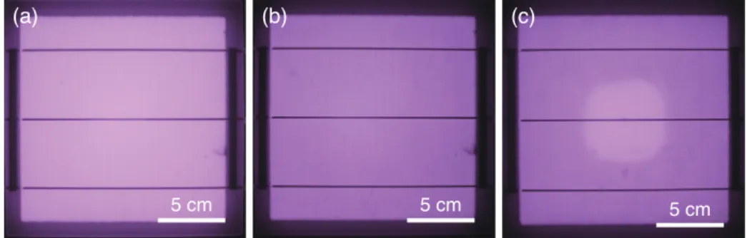
In Figure 4, panels (a) and (b) show the EL images of SHJ PV modules before and after PID testing, respectively, for PID tests in which a negative bias of −1000 V was applied for 32 days. The EL image was slightly darker over the entire region after the PID test. The loss in luminescence was not accompanied by changes in the diode characteristics, as mentioned above, implying that the loss is not related to an enhancement of the non-radiative recombination processes but originates from enhanced optical losses. Figure 4c shows the EL image of a module after a PID test in which a negative bias of −2000 V was applied for 21 days. A characteristic bright, circular pattern can be seen in the middle of the cell; this indicates that the optical loss was non-uniform. This is consistent with the results of the EQE measurement shown in Figure 2. This pattern could also be seen by eye under light from a fluorescent lamp.
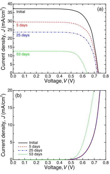
We also investigated the progression behavior during extremely severe PID tests with both a very high bias of −2000 V and very long durations of up to 53 days. Figure 5 shows representative one-sun-illuminated and dark J–V characteristics of an SHJ PV module before and after the PID tests for 5, 25, and 53 days. Figure 6 shows changes in the Jsc/Jsc,0, Voc/Voc,0, FF/FF0, and Pmax/Pmax,0 values of three identical SHJ PV modules undergoing PID tests with the same bias and under the same temperature conditions. Until the length of the PID test reached approximately 30 days, the degradation was characterized only by a reduction in
the Jsc. After about 30 days, the Jsc reduction started to saturate. As the PID tests continued, however, the modules started to exhibit not only an additional reduction in the Jsc but also a moderate reduction in the Voc. This indicates that under severe enough conditions SHJ PV modules undergo another PID mode characterized by reductions in both the Jsc and the Voc. In contrast, the FF increased slightly, which compensates a fraction of the additional degradation. These Voc and Jsc reductions were accompanied by an increase in the saturation current density (Figure 5b), which indicates that the reductions are caused by enhanced bulk and/or interfacial recombination.
3.2. XAFS spectroscopy
To elucidate the root cause of the optical loss, we performed UV-Vis-NIR spectroscopy measurements on a pristine EVA encapsulant sample and an EVA encapsulant sample taken from a degraded PV module; we also conducted XAFS spectroscopy measurements on the front IWO layer of a degraded SHJ PV cell. There were no significant additional optical losses in the EVA sample taken from the degraded module (not shown here). In this section, we therefore focus on the XAFS spectroscopy results. In this XAFS investigation, both XANES and EXAFS results were analyzed in detail.
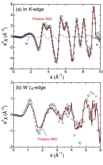
Figure 7 shows the In K-edge and W L3-edge XANES spectra obtained from the front IWO film of an SHJ PV cell degraded in a PID test in which a negative bias of −2000 V was applied for 53 days. The degraded module exhibited a noteworthy reduction in the Jsc and a moderate decrease in the Voc. For a pristine IWO sample, the In K-edge XANES spectrum was almost identical to that of a standard indium oxide (In2O3) sample (not shown here), indicating that In atoms in the pristine IWO have almost the same chemical states as those in the standard In2O3 sample. For the analysis of the In K-edge XANES spectrum of the degraded IWO film, we assumed that In atoms exist in both their initial state and in their chemically reduced state. This assumption seems to be valid because a good fit was obtained by using the In K-edge XANES spectrum of the pristine IWO and the spectrum of the In metal standard sample; this enables the ratio of chemically reduced In to non-reduced In atoms to be estimated. The best fit (indicated by the black solid line in Figure 7a) was obtained when the composition of the material was approximately 24% metallic In. This indicates that 24% of the In atoms in the sample were chemically reduced into metallic In. We also performed the same analysis for the W L3-edge XANES spectra, for which we assumed that W atoms in their initial state and chemically reduced metallic W atoms coexist in the degraded IWO film. The W L3-edge XANES spectrum of the pristine IWO sample had the same peak position as that of a standard tungsten oxide (WO3) sample (not shown here), suggesting that the W in the IWO has similar chemical states to those of W in WO3. However, there was a difference in the peak intensity, implying that the chemical states of W in the IWO sample were modified. This may be because the amount of WO3 in the IWO film was only a few atomic percent or below and because most W atoms were almost completely isolated from other W atoms. The degraded IWO sample showed a very similar W L3-edge XANES spectrum to that of the pristine IWO sample, which indicates that the W chemical states were unchanged. The best fit
shown in Figure 7b was obtained when the W content was zero, implying that no W atoms were chemically reduced.
Figure 8 shows In K-edge k3-weighted and W L3-edge k2-weighted EXAFS spectra obtained from the degraded IWO sample (the same samples as used in the XANES analysis). In this analysis of the EXAFS spectra, good fits were obtained with the same assumption as for the analysis of the XANES spectra. For the In K-edge k3-weighted EXAFS spectra, the spectrum of the pristine IWO sample was almost the same as that of the standard In2O3 sample (not shown here). For the spectrum shown in Figure 8a, the best fit was acquired when the metallic In content was approximately 33%. This result indicates that approximately 33% of the In atoms in the sample were chemically reduced. For the W L3-edge k2-weighted EXAFS spectra, the spectrum of the degraded IWO sample was very similar to that of the pristine IWO sample, which is a similar observation as made for the W L3-edge XANES spectra. The best fit was obtained when the W content was zero. This implies that generally no W atoms were chemically reduced, which is the same as the findings obtained from the W L3-edge XANES spectrum.
3.3. D-SIMS measurements for Na
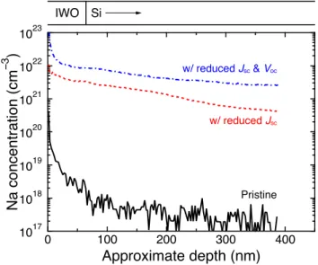
PID, which occurs in several different types of PV modules under negative bias, such as in conventional p-type c-Si [10–14], n-type rear-emitter c-Si [20], n-type IBC c-Si [22], a-Si [24, 25], CIGS [26–28], and CdTe [28, 29] PV modules, has been associated with Na. SHJ PV modules were found to undergo PID under negative bias; thus, it is likely that Na plays an important role. We performed D-SIMS measurements of Na in two degraded cells, namely one with only a reduction in Jsc and one with reductions in both the Jsc and Voc.
Figure 9 shows the D-SIMS profiles of Na in a cell degraded in PID tests in which a negative bias of −2000 V was applied for either 6 or 53 days. The former cell exhibited only a Jsc reduction, while the latter cell exhibited reductions in both the Jsc and Voc. For comparison, a D-SIMS profile of Na in a pristine cell is also shown. The Na concentration reported in Figure 9 was roughly estimated by using the ZnO:Na standard sample. The pristine sample showed a Na concentration on the order of 1019–1020 cm−3 for the surface region; this high concentration was probably caused by contaminants including Na on the cell surface. In the bulk region, the cell showed a low concentration of Na on the order of 1017 cm−3 or lower. However, in the sample that showed a reduction in the Jsc only, the Na concentration was much higher over the entire investigated region. Meanwhile, the sample with reductions in both the Jsc and the Voc showed a further noteworthy increase in the Na concentration. Generally, Na is known as a “lifetime killer” in c-Si and is detrimental to the performance of Si solar cells [34]. Therefore increased concentrations of Na atoms may have a detrimental effect on SHJ PV cells. It should be noted that the D-SIMS measurements were disturbed by a matrix effect and a surface mixing effect, which is known as the knock-on effect. The latter may lead to the overestimation of the Na concentration in the bulk region of the samples. In addition, the measurements were disturbed by the textured surfaces.
3.4. SEM investigation
observation of the surface region of a cell degraded by a PID test in which a negative bias of −2000 V was applied for 53 days. Figure 10 shows the SEM images of a pristine cell and of the degraded cell. The surface of the degraded cell appears to have been degraded, indicating that the continuity of the IWO film was disrupted by the PID. There is also a possibility that the a-Si passivation film was also degraded, leading to a significant reduction in the passivation quality. If the IWO film were degraded, as shown in Figure 10b, an increase in the series resistance (Rs) would be expected; however, such an increase was not observed. It is possible that the IWO film was degraded when the encapsulation material was delaminated for subsequent analyses. However, we conclude that the IWO film was likely significantly damaged during the PID test, because the pristine cell, in which the encapsulation material was also delaminated for comparison, showed no degradation of the IWO film.
In the energy dispersive X-ray spectroscopy measurements, Na (along with Si, In, and oxygen) was detected on the surface of the degraded cell, while no Na signal was detected on the surface of the pristine cell (not shown). This observation is evidence that the Na concentration increases during PID testing, which is consistent with the results of the D-SIMS measurements.
3.5. Effect of the use of an ionomer encapsulant
To determine a possible measure for preventing PID in SHJ PV modules, we performed the PID tests on an SHJ PV module using an ionomer encapsulant, which has a considerably higher volume resistivity (1016 Ω·cm) compared with that of the EVA encapsulant used in this study. Thanks to their high volume resistance, ionomer encapsulants can effectively prevent PID from occurring in several kinds of PV modules, such as p-type c-Si [35], n-type front-emitter c-Si [15], and CIGS [27] PV modules. Figure 11 shows the dependence of Pmax/Pmax,0 of the SHJ PV modules with the standard EVA encapsulant and with the ionomer encapsulant on the PID testing duration. The modules were stressed under a negative bias of −2000 V, which is a severe stress condition. In the EVA modules, Pmax/Pmax,0 was reduced to approximately 70% after 20 days. Conversely, the Pmax/Pmax,0 value of the ionomer module exhibited only a little degradation even after a longer PID test of 58 days, thereby demonstrating the excellent PID-suppression capabilities of the ionomer encapsulant. This PID-suppression capability is likely caused by a significantly reduced leakage current owing to the high volume resistance of the ionomer encapsulant.
4. Discussion
4.1. Degradation behavior of SHJ PV modules
Previous studies [18, 30–32] have shown that commercial SHJ PV modules have a far higher resistance to PID in accelerated PID tests. In these studies, the details of the module’s components were not disclosed, so the actual reason for the PID was not clarified. Generally, studies using commercially completed PV modules face this problem. To overcome this, it is necessary to identify the encapsulation materials. In this study, we attempted to clarify the actual effect of PID on SHJ PV cells by using standard, low-cost encapsulation materials that have
been confirmed to not be capable of preventing PID.
As shown in Figure 1, we found that under a negative bias, SHJ PV modules underwent the sort of PID that is mainly characterized by a reduction in the Jsc. This suggests that SHJ PV modules may suffer from PID characterized by a Jsc reduction when prepared with conventional low-cost encapsulation materials. As shown in Figure 3, the rate of degradation increases with increasing bias. The reduction in the
Jsc was not caused by recombination losses but optical losses, since the EQE of the degraded SHJ PV modules was reduced over the entire wavelength range, as shown in Figure 2. The dark J–V characteristics of the degraded modules were almost unchanged before and after the PID test (Figure 1b). This, too, suggests that there was no significant increase in the recombination losses. This PID, mainly caused by optical losses, is different from all the other PID-related phenomena reported so far (while PID in thin-film a-Si PV modules is partly affected by additional optical losses, other loss mechanisms dominate [25]). A possible reason behind the reduced
Jsc will be discussed in detail in Section 4.2.
The non-uniformity of the optical loss over the entire cell’s area is shown in Figures 2 and 4. The exact reason of the non-uniformity is currently unclear; however, it may be related to the electric field distribution during the PID tests. In actual PV modules, which include several tens of cells, the effect of the electric field distribution is expected to be greater than that in one-cell modules. For example, cells located near the module’s edge probably degrade more readily compared with cells located near the center. Additionally, the EL results indicate that the distribution of the degree of optical loss can be easily identified by using EL measurements. EQE and Jsc mappings would probably also be effective for characterizing the PID behavior in a more quantitative way.
In extremely severe PID tests with a very high bias and with a very long testing duration, the SHJ PV modules were found to suffer not only from a further reduction in the Jsc but also a moderate reduction in the Voc, as shown in Figures 5 and 6. These additional reductions in the Jsc and the Voc were accompanied by an enhanced saturation current density, which suggests that these reductions were mainly caused by an enhancement in the interfacial and/or bulk recombination. In actual PV systems, such a moderate reduction in the Voc would likely only have a minor effect on the efficiency of the string; conversely, the additional reduction in the Jsc would likely have a detrimental effect on the efficiency of the string. This is because a Voc reduction in a cell only slightly reduces the maximum voltage of the string in which the cell is included; however, a Jsc reduction in a cell generally has a substantial effect on the efficiency of the system because the lowest Jsc limits the current flowing through the entire string.
In the D-SIMS measurement, a significantly increased Na concentration was observed in a degraded PV module with reductions in both the Jsc and the Voc. The accumulating Na probably reduced the minority-carrier lifetime and thus the Jsc and the Voc were reduced. The Na build-up in the c-Si region is therefore a potential reason for the Voc reduction. The presence of Na is known to have a very significant, detrimental effect in c-Si as it introduces a defect level close to the mid-gap and has a large capture cross section for minority carriers [34, 36]. It is also possible that a-Si was damaged by the PID, as indicated by the results presented in Figure 10b.
Such damage is expected to degrade the passivation quality, and therefore significantly reduce the Jsc and Voc. Note that the results of our D-SIMS measurements were disturbed by the knock-on effect and the surface texturing of the cells. More accurate evaluation is required to completely understand the phenomenon.
Because our cells had a rear-emitter configuration, the Na introduced into the surface region of the cells only causes reductions in the Jsc and the Voc and does not affect the FF. However, SHJ cells with front-emitter configurations are expected to also show a reduction in the FF, since their depletion region is located within the front surface region of the c-Si base and because the Na introduced at the c-Si front surface should enhance recombination in the depletion region.
It should be noted that the Jsc reduction that coincides with the Voc reduction can likely only be observed in very severe PID tests in which a high bias is applied for a long time. These additional reductions are therefore not expected to occur in actual PV systems. However, if SHJ PV modules were deployed in a PV system with such extremely severe conditions, reductions in both the Voc and the Jsc should be prevented; this could be achieved, for example, by using high-electric-resistance encapsulants such as ionomer encapsulants, as shown in Figure 11.
4.2. Root cause of optical loss
To determine the root cause of the optical loss, we performed UV-Vis-NIR spectroscopy of a pristine EVA encapsulant sample and an EVA encapsulant sample taken from a degraded PV module, and conducted XAFS spectroscopy measurements on the IWO layer of the degraded cell. The optical loss in the EVA layer was not significant and too small to explain the Jsc reduction that was actually observed. Increased optical loss in the cover glass may be the reason behind the Jsc reduction. However, increased optical losses in the cover glass have not yet been reported. In this section, we thus mainly discuss the results of the XAFS spectroscopy measurements of the front IWO layer of the degraded cell.
By analyzing the XANES and EXAFS results for the degraded IWO layer, we found that the results of the 53-day-long PID test show that 24–33% of the In atoms were chemically reduced and were converted into metallic In. Conversely, no detectable increase in the amount of metallic W was found in the degraded IWO film. These observations strongly suggest that the root cause of the optical loss is the darkening of the front IWO layer caused by the formation of metallic In precipitates. The darkened IWO layer intercepts the incident light, leading to a significant reduction in the Jsc. There was a possibility that the In precipitates affected the electrical characteristics of the TCO films; however, no significant change in FF was actually seen after the PID tests as shown in Figs. 5 and 6. This may be because metallic In precipitates are good conductors.
To explain the formation of the metallic In precipitates, we considered the chemical reduction of In2O3. It has been reported that indium-oxide-based TCO films are relatively readily reduced by exposure to a strongly reducing environment such as hydrogen plasma and that metal precipitates can be formed as a result [37– 43]. As we applied a negative bias to the cells in our PID tests, the cells corresponded to the cathode in oxidation-reduction reactions. Chemical reduction
reactions should therefore occur in the surface region of the cells’ front IWO layer. One potential reaction is the chemical reduction of Na ions, which may originate from the cover glass [12] and/or contaminants on the cell surface [44]: Na+ + e− → Na. This is based on the D-SIMS measurements, which showed increased Na concentrations in the surface region of the IWO after the PID tests, as shown in Figure 9; this strongly suggests that the reaction actually occurred in the front IWO film. Such Na atoms may induce the formation of metal precipitates as a result of their reoxidation process. In our experiment, the effect of moisture ingress could be neglected because the relative humidity was very low. However, assuming that the moisture originally contained in the EVA encapsulant affects the chemical reduction process of In2O3, there may be another possible formation mechanism underpinning the formation of the metallic In precipitates. In a previous study on PID in superstrate a-Si thin-film PV modules, the delamination of fluorine-doped tin oxide (SnO2:F) layers was reportedly induced by a negative potential and moisture ingress [24]. To explain this phenomenon, Jansen et al. [45] proposed that elemental hydrogen (H) atoms, which have a very high reducing power, are formed by reactions between Na atoms and moisture, causing the delamination of the SnO2:F films. On the basis of this explanation, we propose that metallic In is formed during the chemical reduction of In2O3, which is induced by elemental H atoms. Much additional work is, however, required to completely understand the formation mechanism of the metallic In and its effects on the optical properties of IWO films.
The chemical reduction may also lead to the destruction of the IWO film, as shown in Figure 10b. This may increase the Rs and may, therefore, reduce the FF. Additionally, the chemical reduction may also contribute to a reduction in the Jsc, because the IWO film serves not only as an electrode but also as an antireflection coating. However, there was no significant reduction in the FF, as shown in Figure 6; thus, the Jsc loss was mainly caused by the shadowing loss from the In precipitates. As mentioned above, the IWO film may have peeled off from the surface when the EVA was removed from the cell for subsequent analyses. However, in either case, the IWO layer was considered to be significantly damaged and became brittle owing to the PID test. It is also possible that the underlying a-Si passivation layer was damaged, thereby significantly degrading the passivation quality and therefore significantly reducing the Jsc and the Voc.
4.3. Comparison of resistance to PID of SHJ PV modules and other types of PV modules
From the viewpoint of large-scale PV system installations, it is very important to determine the lifetime of PV modules based on the acceleration factor of PID tests. However, we could not determine the acceleration factor of our PID test because of insufficient field data for PID. Instead, we discuss the resistance to PID of the SHJ PV modules by comparing the PID test results of the SHJ PV modules with those of other types of modules.
We have previously reported PID test results for PID-prone p-type c-Si [27], conventional superstrate-type a-Si thin-film [27], CIGS thin-film [27], n-type front-emitter c-Si [15], and n-type rear-emitter c-Si [20] PV modules. Except for
the a-Si thin-film module, these PV modules had the same module configuration and the same encapsulation materials (the a-Si thin-film module had a superstrate configuration; thus, there was no encapsulant between the front glass and the cells). Further, all the bias, temperature, and humidity conditions were the same as those used in this study. After 1 day of PID testing, the Pmax/Pmax,0 value of the a-Si [27], CIGS [27], and n-type rear-emitter c-Si [20] PV modules decreased to 0.23, 0.95, and 0.93, respectively. When the PID tests were 2 days long, however, the
Pmax/Pmax,0 for the p-type c-Si [27] and n-type front-emitter c-Si [15] PV modules decreased to 0.04–0.4 and 0.85, respectively. In contrast, the SHJ PV modules exhibited little degradation after the 2-day-long PID test. This result suggests that the SHJ PV modules have a higher resistance to PID than other types of cells. This advantage of the SHJ PV modules suggests that further installation of this type of PV module should be promoted.
On the basis of the proposed mechanism moisture ingress is expected to strongly affect the degradation behavior and therefore the cells’ resistance to PID, although the effect could not be investigated in this study since all the PID tests were performed in a dry environment. Therefore the high resistance to PID reported here may be an overstatement, and there is a probability that the resistance to PID is reduced in a highly humid environment. Thus, PID in SHJ PV modules is still an important issue.
It should be noted that PID in SHJ PV modules is irreversible, which is a disadvantage. Furthermore, the PID can substantially affect the efficiency of the entire string, because the PID is characterized by a reduction in the Jsc and a reduced Jsc may limit the current in the entire string. Consequently, it is important to determine possible measures to prevent PID.
4.4. Potential measures for preventing PID
PID in SHJ PV modules was found to be effectively prevented by the use of an ionomer encapsulant, demonstrating that the high reliability of SHJ PV modules can be further improved by using encapsulants with a high electrical resistance. This protective effect is already well known for preventing PID in other types of PV modules [15, 27, 35]; this effect is in part caused by the suppression of Na migration. The PID-suppression effect observed in this study is likely caused by a significant reduction in Na migration, which is consistent with the proposed mechanism presented in Section 4.2.
The use of alternative TCO materials may be another possible preventive measure. In PID in SHJ PV modules, the chemical reduction of oxidized species plays a crucial role, and, thus, it is important to prevent this chemical reduction to prevent PID. Regarding PID in CIGS PV modules, however, it appears that no darkening of the front zinc-oxide (ZnO)-based TCO layers occurs during PID tests despite a significantly increased Na concentration in the ZnO layers [27]. This is likely because ZnO-based TCO films are resistant to chemical reduction compared with indium oxide-based TCO [43]. This implies that the PID in SHJ PV modules can be prevented by the use of another TCO material that is highly resistant to chemical reduction. The use of multilayered front TCO films, for example, composed of ZnO and In2O3-based TCO, may also be effective for preventing PID.
The basic idea is to prevent the chemical reduction of In atoms in the bottom layer by using a chemical-reduction-resistant top ZnO layer while minimizing the influence on the interfacial properties at the interface between the TCO and the underlying a-Si layer.
The use of a barrier layer for Na may also be effective for reducing the PID effect. Adachi et al. [46] have reported that silicon oxide (SiOx) barrier layers deposited on SHJ cells by plasma-enhanced chemical vapor deposition improve the cells’ resistances to damp-heat stress by reducing the ingress of both moisture and Na into the layers below the barrier layers. The use of barrier layers is thus a reasonable approach given our proposed degradation mechanism.
5. Conclusions
Using a rapid PID test we investigated PID in SHJ PV modules with low-cost encapsulation materials. After the PID tests, the SHJ modules exhibited a reduction in the Jsc, revealing that SHJ PV modules undergo PID that is characterized by a reduction in the Jsc. EQE and dark J–V measurements revealed that the Jsc loss was not caused by recombination losses but by optical losses. The degradation was irreversible, unlike PID in conventional p-type c-Si PV modules. Further, the degradation rate increased with the applied bias. By performing PID tests with a high bias and long stress duration, we also found that SHJ PV modules suffer not only from a further Jsc reduction but also from a moderate Voc reduction. These Jsc and Voc losses can probably be attributed to a reduced carrier lifetime caused by Na being introduced into the surface region of the c-Si base.
To determine the root cause of the optical loss, we performed XAFS spectroscopy on the IWO film of an SHJ PV cell that was significantly degraded during PID testing. From the XANES and EXAFS results, we found the formation of metallic In in the degraded IWO, demonstrating that the root cause of the optical loss is the darkening of the front IWO films caused by the precipitation of metallic In. We propose that Na atoms and/or other reductants that are produced during the oxidation of the Na atoms induce the formation of the metallic In precipitates. Additional work is required to completely understand the formation mechanism of the metallic In and its effects on the optical properties of the IWO films.
We also showed that SHJ PV modules have a notably high resistance to PID compared with conventional p-type c-Si, n-type front-emitter c-Si, n-type rear-emitter c-Si, a-Si thin-film, and CIGS thin-film PV modules. This demonstrates that SHJ PV modules have a high resistance to PID even if they are prepared using typical low-cost encapsulation materials. The already high reliability of SHJ PV modules can be further improved by using encapsulants with high electrical resistances, such as ionomer encapsulants. Based on our explanations, PID may be reduced in various ways, such as by changing the TCO material or using a barrier layer against Na.
Acknowledgments
The authors would like to thank Dr. Kohjiro Hara of National Institute of Advanced Industrial Science and Technology (AIST), Japan, for performing the
EQE measurements and Sachiko Jonai of AIST, Japan, for providing information about the volume resistivity of the EVA and ionomer sheets. The authors would also like to thank Du Pont-Mitsui Polychemicals Co., Ltd., Japan, for providing the ionomer-type PV module encapsulants. This work was supported by the New Energy and Industrial Technology Development Organization, Japan.
References
[1] de Wolf S, Descoeudres A, Holman ZC, Ballif C. High-efficiency silicon heterojunction solar cells: A review. Green 2012; 2: 7–24.
[2] Mishima T, Taguchi M, Sakata H, Maruyama E. Development status of high- efficiency HIT solar cells. Sol. Energy Mater. Sol. Cells 2011; 95: 18–21. [3] Kinoshita T, Fujishima D, Yano A, Ogane A, Tohoda S, Matsuyama K,
Nakamura Y, Tokuoka N, Kanno H, Sakata H, Taguchi M, Maruyama E. The approaches for high efficiency HIT solar cell with very thin (<100 μm) silicon wafer over 23%, In Proc. 26th European Photovoltaic Solar Energy
Conf. Exhib., 2011, pp. 871– 874.
[4] Taguchi M, Yano A, Tohoda S, Matsuyama K, Nakamura Y, Nishiwaki T, Fujita K, Maruyama E. 24.7% record efficiency HIT solar cell on thin silicon wafer. IEEE J. Photovolt. 2014; 4: 96–99.
[5] Adachi D, Hernández JL, Yamamoto K. Impact of carrier recombination on fill factor for large area heterojunction crystalline silicon solar cell with 25.1% efficiency. Appl. Phys. Lett. 2015; 107: 233506.
[6] Masuko K., Shigematsu M, Hashiguchi T, Fujishima D, Kai M, Yoshimura N, Yamaguchi T, Ichihashi Y, Mishima T, Matsubara N, Yamanishi T, Takahama T, Taguchi M, Maruyama E, Okamoto S. Achievement of more than 25% conversion efficiency with crystalline silicon heterojunction solar cell. IEEE
J. Photovolt. 2014; 4: 1433–1435.
[7] Yoshikawa K, Kawasaki H, Yoshida W, Irie T, Konishi K, Nakano K, Uto T, Adachi D, Kanematsu M, Uzu H, Yamamoto K. Silicon heterojunction solar cell with interdigitated back contacts for a photoconversion efficiency over 26%. Nat. Energy 2017; 2: 17032.
[8] SEMI PV Group Europe. International Technology Roadmap for Photovoltaic (ITRPV). http://www.itrpv.net/, 2017 (accessed 28.06.17). [9] Luo W, Khoo YS, Hacke P, Naumann V, Lausch D, Harvey SP, Singh JP,
Chai J, Wang Y, Aberle AG, Ramakrishna S. Potential-induced degradation in photovoltaic modules: a critical review. Energy Environ. Sci. 2017; 10: 43–68. [10] Pingel S, Frank O, Winkler M, Daryan S, Geipel T, Hoehne H, Berghold J. Potential induced degradation of solar cells and panels. In Proc. 35th IEEE
Photovoltaic Specialists Conf., 2010, pp. 2817–2822.
[11] Berghold J, Frank O, Hoehne H, Pingel S, Richardson S, Winkler M. Potential induced degradation of solar cells and panels. In Proc. 25th
European Photovoltaic Solar Energy Conf. Exhib./5th World Conf. Photovoltaic Energy Conversion, 2010, pp. 3753–3759.
[12] Hacke P, Kempe M, Terwilliger K, Glick S, Call N, Johnston S, Kurtz S, Bennett I, Kloos M. Characterization of multicrystalline silicon modules with system bias voltage applied in damp heat. In Proc 25th European Photovoltaic Solar Energy Conf. Exhib./5th World Conf. Photovoltaic Energy Conversion, 2010, pp. 3760–3765.
[13] Naumann V, Lausch D, Graff A, Werner M, Swatek S, Bauer J, Hähnel A, Breitenstein O, Großer S, Bagdahn J, Hagendorf C. The role of stacking faults for the formation of shunts during potential-induced degradation of crystalline Si solar cells. Phys. Status Solidi: Rapid Res. Lett. 2013; 7: 315–318.
[14] Naumann V, Lausch D, Hähnel A, Bauer J, Breitenstein O, Graff A, Werner M, Swatek S, Großer S, Bagdahn J, Hagendorf C. Explanation of potential-induced degradation of the shunting type by Na decoration of stacking faults in Si solar cells. Sol. Energy Mater. Sol. Cells 2014; 120: 383– 389.
[15] Hara K, Jonai S, Masuda A. Potential-induced degradation in photovoltaic modules based on n-type single crystalline Si solar cells. Sol. Energy Mater.
Sol. Cells 2015; 140: 361–365.
[16] Yamaguchi S, Masuda A, Ohdaira K. Progression of rapid potential-induced degradation of n-type single-crystalline silicon photovoltaic modules. Appl.
Phys. Express 2016; 9: 112301.
[17] Bae S, Oh W, Lee KD, Kim S, Kim H, Park N, Chan S-I, Park S, Kang Y, Lee H-S, Kim D. Potential induced degradation of n-type crystalline silicon solar cells with p+ front junction. Energy Sci. Eng. 2017; 5: 30–37.
[18] Hara K, Ogawa K, Okabayashi Y, Matsuzaki H, Masuda A. Influence of surface structure of n-type single-crystalline Si solar cells on potential-induced degradation. Sol. Energy Mater. Sol. Cells 2017; 166: 132– 139.
[19] Barbato M, Barbato A, Meneghini M, Tavernaro G, Rossetto M, Meneghesso G. Potential induced degradation of N-type bifacial silicon solar cells: An investigation based on electrical and optical measurements. Sol. Energy
Mater. Sol. Cells 2017; 168: 51–61.
[20] Yamaguchi S, Masuda A, Ohdaira K. Changes in the current density-voltage and external quantum efficiency characteristics of n-type single-crystalline silicon photovoltaic modules with a rear-side emitter undergoing potential-induced degradation. Sol. Energy Mater. Sol. Cells 2016; 151: 113– 119.
[21] Swanson R, Cudzinovic M, DeCeuster D, Desai V, Jürgens J, Kaminar N, Mulligan W, Rodrigues-Barbosa L, Rose D, Smith D, Terao A, Wilson K. The surface polarization effect in high-efficiency silicon solar cells. In Tech.
Dig. 15th Int. Photovoltaic Sci. Eng. Conf., 2005, pp. 410–411.
[22] Naumann V, Geppert T, Großer S, Wichmann D, Krokoszinski H-J, Werner M, Hagendorf C. Potential-induced degradation at interdigitated back contact solar cells. Energy Procedia 2014; 55: 498–503.
[23] Halm A, Schneider A, Mihailetchi VD, Koduvelikulathu LJ, Popescu LM, Galbiati G, Chu H, Kopecek R. Potential-induced degradation for encapsulated n-type IBC solar cells with front floating emitter. Energy
Procedia 2015; 77: 356–363.
[24] Osterwald CR, McMahon TJ, del Cueto JA. Electrochemical corrosion of SnO2: F transparent conducting layers in thin-film photovoltaic modules. Sol.
Energy Mater. Sol. Cells 2003; 79: 21–33.
[25] Masuda A, Hara Y. Potential-induced degradation of thin-film Si photovoltaic modules. Jpn. J. Appl. Phys. 2017; 56: 04CS04.
[26] Fjällström V, Salomé PMP, Hultqvist A, Edoff M, Jarmar T, Aitken BG, Zhang K, Fuller K, Williams CK. Potential-induced degradation of CuIn1−xGaxSe2 thin film solar cells. IEEE J. Photovolt. 2013; 3: 1090–1094.
[27] Yamaguchi S, Jonai S, Hara K, Komaki H, Shimizu-Kamikawa Y, Shibata H, Niki S, Kawakami Y, Masuda A. Potential-induced degradation of Cu(In,Ga)Se2 photovoltaic modules. Jpn. J. Appl. Phys. 2015; 54: 08KC13. [28] Hacke P, Terwilliger K, Glick SH, Perrin G, Wohlgemuth J, Kurtz S,
Showalter K, Sherwin J, Schneller E, Barkaszi S, Smith R. Survey of potential-induced degradation in thin-film modules. J. Photon. Energy 2015;
5: 053083.
[29] Hacke P, Spataru S, Johnston S, Terwilliger K, VanSant K, Kempe M, Wohlgemuth J, Kurtz S, Olsson A, Propst M. Elucidating PID degradation mechanisms and in situ dark I–V monitoring for modeling degradation rate in CdTe thin-film modules. IEEE J. Photovolt. 2016; 6: 1635–1640.
[30] Xiong Z, Walsh TM, Aberle AG. PV module durability testing under high voltage biased damp heat conditions. Energy Procedia 2011; 8: 384–389. [31] Ishiguro T, Kanno H, Taguchi M, Okamoto S. Study on PID resistance of
HIT PV modules. presented at 2013 Photovoltaic Module Reliability
Workshop, 2013.
[32] Riedel N, Pratt L, Moss E, Yamasaki M. 600 hour potential induced degradation (PID) testing on silicon, CIGS, and HIT modules. presented at
2015 NREL Photovoltaic Reliability Workshop, 2015.
[33] Yamaguchi S, Yamamoto C, Ohdaira K, Masuda A. Reduction in the short-circuit current density of silicon heterojunction photovoltaic modules subjected to potential-induced degradation tests. Sol. Energy Mater. Sol.
Cells 2017; 161: 439–443.
[34] Osinniy V, Bomholt P, Larsen AN, Enebakk E, Søiland A-K, Tronstad R, Safir Y. Factors limiting minority carrier lifetime in solar grade silicon produced by the metallurgical route. Sol. Energy Mater. Sol. Cells 2011; 95: 564–572.
[35] Kapur J, Stika KM, Westphal CS, Norwood JL, Hamzavytehrany B. Prevention of potential-induced degradation with thin ionomer film. IEEE J.
Photovolt. 2015; 5: 219–223.
[36] Chen J-W, Milnes AG. Energy levels in silicon. Ann. Rev. Mater. Sci. 1980;
10: 157–228.
[37] Fan JCC, Goodenough JB. X-ray photoemission spectroscopy studies of Sn-doped indium-oxide films. J. Appl. Phys. 1977; 48: 3524–3531.
[38] Kitagawa M, Mori K, Ishihara S, Ohno M, Hirao T, Yoshioka Y, Kohiki S. Interaction of hydrogenated amorphous silicon films with transparent conductive films. J. Appl. Phys. 1983; 54: 3269–3271.
[39] Major S, Kumar S, Bhatnagar M, Chopra KL, Effect of hydrogen plasma treatment on transparent conducting oxides. Appl. Phys. Lett. 1986; 49: 394– 396.
[40] Banerjee R, Ray S, Basu N, Batabyal AK, Barua AK. Degradation of tin-doped indium-oxide film in hydrogen and argon plasma. J. Appl. Phys. 1987; 62: 912–916.
[41] Oesterlein R, Krokoszinski H-J. Optical dispersion in
electron-beam-evaporated indium tin oxide thin films. Thin Solid Films 1989; 175: 241–247.
[42] Minami T, Sato H, Nanto H, Takata S. Heat treatment in hydrogen gas and plasma for transparent conducting oxide films such as ZnO, SnO2 and indium tin oxide. Thin Solid Films 1989; 176: 277–282.
[43] Drevillon B, Kumar S, Roca i Cabarrocas P, Siefert JM. In situ investigation of the optoelectronic properties of transparent conducting oxide/amorphous silicon interfaces. Appl. Phys. Lett. 1989; 54: 2088–2090.
[44] Naumann V, Lausch D, Hagendorf C. Sodium decoration of PID-s crystal defects after corona induced degradation of bare silicon solar cells. Energy
Procedia 2015; 77: 397–401.
[45] Jansen KW, Delahoy AE. A laboratory technique for the evaluation of electrochemical transparent conductive oxide delamination from glass substrates. Thin Solid Films 2003; 423: 153–160.
[46] Adachi D, Terashita T, Uto T, Hernández JL, Yamamoto K. Effects of SiOx barrier layer prepared by plasma-enhanced chemical vapor deposition on improvement of long-term reliability and production cost for Cu-plated amorphous Si/crystalline Si heterojunction solar cells. Sol. Energy Mater. Sol.
Figure captions
Figure 1. Representative (a) one-sun-illuminated and (b) dark J–V curves of SHJ
PV modules before and after PID tests in which a negative bias of −1000 V was applied for 9, 18, and 32 days. The inset figure shows the dependence of the Jsc/Jsc,0 value on the PID testing duration.
Figure 2. EQE characteristics of a pristine SHJ PV module and of a module after
PID testing for 13 days with an applied negative bias of −1000 V. For the degraded module, EQE values were extracted from two positions, namely from the center and the edge of the cell. The illuminated area in these EQE measurements was 10 × 10 mm2. As a noteworthy case, the EQE of a degraded module from a PID test with a very high bias of −2000 V is also shown in this figure; this EQE value was obtained from a significantly degraded area of the module.
Figure 3. Applied-bias dependence of several degradation characteristics of SHJ
PV modules: (a) Jsc/Jsc,0, (b) Voc/Voc,0, (c) FF/FF0, and (d) Pmax/Pmax,0. The black solid lines and red dashed lines show the data obtained in PID tests with −1000 and −2000 V, respectively. Data points indicated with the same kind of symbol were obtained from the same sample. The solid and dashed lines are included as guides for the eye.
Figure 4. EL images of SHJ PV modules (a) before and (b) after PID tests in which
a negative bias of −1000 V was applied for 32 days and (c) after PID tests in which a negative bias of −2000 V was applied for 21 days.
Figure 5. Representative (a) one-sun-illuminated and (d) dark J–V curves of SHJ
PV modules before and after PID tests in which a negative bias of −2000 V was applied for 5, 25, and 53 days.
Figure 6. Evolution of the (a) Jsc/Jsc,0, (b) Voc/Voc,0, (c) FF/FF0, and (d) Pmax/Pmax,0 values of SHJ PV modules throughout a relatively long PID test in which a high negative bias of −2000 V was applied. Data points indicated with the same kind of symbol were obtained from the same module. The solid lines are guides for the eye.
Figure 7. (a) In K-edge and (b) W L3-edge XANES spectra obtained from the front IWO film of an SHJ PV cell after a PID test in which a negative bias of −2000 V was applied for 53 days. The experimental data are indicated by open circles. The solid lines were obtained by fitting the XANES spectra by using the data extracted from the pristine IWO film and from the standard In and W samples. The lines designated with “Pristine IWO” and with “In” show the pristine IWO and metallic
In components of the fitting curve, respectively. In panel (b), the best fit was obtained when the W component was zero; therefore, the line for the W component is not shown. The fitting result indicates the formation of an additional metallic In component that accounts for approximately 24% of the total amount of In atoms.
Figure 8. (a) In K-edge k3-weighted and (b) W L
3-edge k2-weighted EXAFS spectra obtained from the front IWO film of an SHJ PV cell after a PID test in which a negative bias of −2000 V was applied for 53 days. The experimental data are indicated by the open circles. The solid lines were obtained by fitting the EXAFS spectra by using the data extracted from the pristine IWO film and from the standard In and W samples. The lines marked with “Pristine IWO” and with “In” show the pristine IWO and metallic In components of the fitting curve, respectively. In panel (b), the best fit was obtained when the W component was zero; therefore, the line for the W component is not shown. The fitting result indicates an additional metallic In component that accounts for approximately 33% of the total amount of In atoms.
Figure 9. Na D-SIMS profiles of a pristine cell and of cells degraded by PID
testing in which a negative bias of −2000 V was applied for 6 and 53 days. The cell degraded for 6 days exhibited only a Jsc reduction while the one degraded for 53 days exhibited reductions in both its Jsc and Voc. The D-SIMS profiles were obtained using the Cs+ primary ion beam with an acceleration voltage of 3 keV, and the corresponding Na concentrations were roughly estimated by using the ZnO:Na standard sample. The bar placed just above the plot area shows the approximate location of the IWO/Si interface, which is based on D-SIMS profiles of In and Si extracted from a pristine SHJ PV cell. The a-Si-based passivation layers were actually located at the IWO/Si interface, and, however, the layers are not shown in the bar because the layers are considerably thinner. The ordinate is on a log scale.
Figure 10. Cross-sectional SEM images of the surface regions of (a) the pristine
SHJ cell and of (b) the SHJ cell degraded during PID testing in which a negative bias of −2000 V was applied for 53 days. The acceleration voltage in the observations was set to 5 keV. The a-Si-based passivation layers were actually located at the IWO/Si interface.
Figure 11. PID-suppression effect of the ionomer encapsulant in a PID test in
which a negative bias of −2000 V was applied. For comparison, data obtained from PV modules with EVA encapsulants are also shown. The solid and dashed lines are guides for the eye.
Fig. 1 40 35 30 25 20 15 10 5 0 Current density, J (mA/cm 2 ) 0.8 0.7 0.6 0.5 0.4 0.3 0.2 0.1 0.0 Voltage,V (V) Initial 9 days 18 days 32 days 1.05 1.00 0.95 0.90 0.85 0.80 Jsc /Jsc,0 30 20 10 0
PID-stress duration (day)
20 15 10 5 0 0.8 0.7 0.6 0.5 0.4 0.3 0.2 0.1 0.0 Initial 9 days 18 days 32 days Voltage,V (V) Current density, J (mA/cm 2 ) (a) (b)
Fig. 2 1.0 0.8 0.6 0.4 0.2 0.0
External quantum efficiency, EQE 400 600 800 1000 1200
Wavelength, λ (nm)
Unaffected
13 days (center)
13 days (edge)
Fig. 3 1.05 1.00 0.95 0.90 0.85 0.80 0.75 0.70 0.65 35 30 25 20 15 10 5 0
PID-stress duration (day)
−1000 V −1000 V −2000 V (a) 1.05 1.00 0.95 0.90 0.85 0.80 0.75 0.70 0.65 35 30 25 20 15 10 5 0
PID-stress duration (day) (b) 1.05 1.00 0.95 0.90 0.85 0.80 0.75 0.70 0.65 35 30 25 20 15 10 5 0
PID-stress duration (day) (d) 1.05 1.00 0.95 0.90 0.85 0.80 0.75 0.70 0.65 Normalized FF, FF/FF 0 35 30 25 20 15 10 5 0
PID-stress duration (day) (c) Normalized Jsc , Jsc /Jsc,0 Normalized Voc , Voc /Voc,0 Normalized Pmax , Pmax /P max,0
Fig. 4 (a) 5 cm (b) 5 cm (c) 5 cm
Fig. 5 40 35 30 25 20 15 10 5 0 0.8 0.7 0.6 0.5 0.4 0.3 0.2 0.1 0.0 Initial 5 days 25 days 53 days Current density, J (mA/cm 2 ) Voltage,V (V) 20 15 10 5 0 0.8 0.7 0.6 0.5 0.4 0.3 0.2 0.1 0.0 Initial 5 days 25 days 53 days Current density, J (mA/cm 2 ) Voltage,V (V) (a) (b)
Fig. 6 (a) (b) (d) (c) 1.2 1.0 0.8 0.6 0.4 0.2 0.0 60 50 40 30 20 10 0
PID-stress duration (day)
1.2 1.0 0.8 0.6 0.4 0.2 0.0 60 50 40 30 20 10 0
PID-stress duration (day)
1.2 1.0 0.8 0.6 0.4 0.2 0.0 60 50 40 30 20 10 0
PID-stress duration (day)
1.2 1.0 0.8 0.6 0.4 0.2 0.0 60 50 40 30 20 10 0
PID-stress duration (day)
Normalized FF, FF/FF 0 Normalized Jsc , Jsc /Jsc,0 Normalized Voc , Voc /Voc,0 Normalized Pmax , Pmax /Pmax,0
Fig. 7
Absorption (arb. units)
27950 27940 27930 27920 Energy (eV) (a) In K-edge Pristine IWO In
Absorption (arb. units)
10230 10220 10210 10200 10190 Energy (eV) (b) W L3-edge Pristine IWO
Fig. 8 -6 -4 -2 0 2 4 6 k 3 ( 3 ) 10 8 6 4 2 0 k ( 1) (a) In K-edge -2 -1 0 1 2 k 2 ( 2 ) 6 5 4 3 2 1 0 k ( 1) (b) W L3-edge Pristine IWO In Pristine IWO
Fig. 9 1017 1018 1019 1020 1021 1022 1023 Na concentration (cm 3 ) 400 300 200 100 0 Approximate depth (nm) IWO Si w/ reduced Jsc & Voc w/ reduced Jsc Pristine
Fig. 10
(a) (b)
3 μm 3 μm
IWO/a-Si stack
Fig. 11 1.05 1.00 0.95 0.90 0.85 0.80 0.75 0.70 0.65 60 50 40 30 20 10 0
PID-stress duration (day)
Ionomer EVA Normalized Pmax , Pmax /Pmax,0