Optical Absorption and Photovoltaic Properties of CdSe
Quantum Dots on TiO
2Electrodes with Different
Morphology
WITOON YINDEESUK
DEPARTMENT OF ENGINEERING SCIENCE
THE UNIVERSITY OF ELECTRO-COMMUNICATIONS
MARCH 2014
Optical Absorption and Photovoltaic Properties of CdSe
Quantum Dots on TiO
2Electrodes with Different
Morphology
by
WITOON YINDEESUK
A Dissertation Submitted in Partial Fulfillment of the
Requirements for the Degree of
DOCTOR OF ENGINEERING
at
THE UNIVERSITY OF ELECTRO-COMMUNICATIONS
MARCH 2014
Optical Absorption and Photovoltaic Properties of CdSe
Quantum Dots on TiO
2Electrodes with Different
Morphology
APPROVED BY THE SUPERVISORY COMMITTEE:
CHAIRPERSON: ASSOC. PROF. Qing Shen
MEMBER: PROF. Taro Toyoda
MEMBER: PROF. Shigeo Hayashi
MEMBER: PROF. Kohji Abe
Copyright
By
WITOON YINDEESUK
2014
i
吸収と光電変換特性
近年半導体量子ドット(semiconductor quantum dot, 略して QD)は、大きな光吸収係 数と双極子モーメントを有し、さらに多重励起子生成効果を示すため、次世代の太陽電 池における高効率増感剤の一つとして注目されている。増感剤はナノ粒子酸化物(今回 は TiO2を適用)電極に吸着され、太陽電池の作用電極基板として使用される。ここで、 ナノ粒子酸化物電極には種々のモルフォロジーを持つものが適用されている。本研究で は、数 10 ナノメートルの粒径を有する TiO2ナノ粒子集合体電極基板と、フォトニック 特性を示す逆オパール(蜂の巣)構造を有する TiO2電極基板を対象とし、CdSe QD を 吸着した2つの電極基板系の光吸収スペクトル特性評価、光電流量子効率スペクトル特 性評価、さらに太陽電池デバイスを形成し光電変換特性評価を行った。CdSe QD の吸 着には Cd+と Se-イオンを交互に吸着する successive ionic layer adsorption and reaction (略 して SILAR)法を適用した。この手法は従来のイオン系が混合した溶液中で行う吸着法 (CBD 法)に比べて、良質で粒径均一性の良い QD が形成出来ることで知られている。こ こで、対象とする基板電極系は半透明・不透明であるため、光吸収測定にはこれらに有 効な光音響法を適用した。光電流量子効率は短絡電流の波長分散から、光電変換は疑似 太陽光を適用する既存のソーラーシミュレータにより評価を行った。 光吸収評価から、CdSe QD の成長と量子閉じ込め効果の出現が判明した。光吸収結 果に対して有効質量近似を適用し、交互のイオン吸着回数(3-14 回)に対する CdSe QD の 粒径変化を求めた。その結果、ナノ粒子集合体電極基板と逆オパール構造電極基板では 粒径の大きさと変化は一致し、5nm から 12nm まで単調に増加し、結晶成長は電極基板 のモルフォロジーには依存しないという結果が得られた。一方光透過率の測定を行った 結果、ナノ粒子集合体電極基板では逆オパール電極に比べて 3 倍ほど CdSe QD の吸着 速度が速いことが判明した。一つの可能性として、ナノ粒子集合体電極基板と逆オパー ル構造電極基板における TiO2の結晶面方位が異なり、QD 吸着速度が異なることが考え られ、今後は基板における各結晶面方位の状態密度の評価が重要となる。続いて光吸収 におけるバンドギャップ以下の光吸収領域の評価から、ナノ粒子集合体電極基板吸着に
ii 構造電極基板作製における、より一層の詳細な条件の検討が必要となる。 光電流量子効率測定から、TiO2の光吸収端下の領域(可視領域)で光電流が観測さ れた。この結果から、CdSe QD の分光増感機能の発現が判明した。CdSe QD の粒径の 増加に伴い、極大値は次第に低エネルギー側にシフトした。ナノ粒子集合体電極基板吸 着に比べ逆オパール構造電極基板吸着では光電流量子効率の大きさはおよそ 1/2 で、吸 着表面積の違いと吸着条件の違いが要因の一つと考えられる。 光電変換特性評価から、いずれの系でも短絡電流は CdSe QD の成長に伴い増加する。 しかし、ナノ粒子集合体電極基板吸着に比べ逆オパール構造電極基板吸着では、短絡電 流の大きさはおよそ 1/2 で、光電流量子効率の違いに対応している。一方開放電圧の値 は両系とも CdSe QD の成長には依存せずほぼ一定値であるが、逆オパール構造電極基 板吸着系ではナノ粒子集合体電極基板吸着系に比べて、およそ 0.1V ほど高いことが判 明した。この事実は、逆オパール構造電極の価電子帯の頂上が、ナノ粒子集合体電極に 比べてエネルギー的に高い位置にあることを示唆している。今後は光電子分光法等を適 用しナノ粒子酸化物基板の電子構造の検討が必要となる。形状因子に関しては、ナノ粒 子集合体電極基板吸着と逆オパール構造電極基板吸着では大きな違いは見られなかった。 以上の光電変換特性評価から、逆オパール構造電極基板吸着系での最大光電変換効率は 1.3%、ナノ粒子集合体電極基板吸着系では 2.7%が得られた。さらに、光電変換効率は デバイスの直列抵抗成分と並列抵抗成分が大きく関与するため、これらの抵抗成分の検 討を行った。その結果、逆オパール構造電極基板吸着系ではナノ粒子集合体電極基板吸 着系に比べ、直列抵抗成分はおよそ 3 倍大きく、並列抵抗成分はおよそ 1.5 倍程度大き いことが判明した。光電変換特性では直列抵抗成分の減少と並列抵抗成分の増大を図る ことが光電変換効率の向上につながるため、電極基板、特に逆オパール構造電極基板吸 着系における CdSe QD との間の界面準位の評価を行い、界面準位の減少を図り直列抵 抗成分の減少と並列抵抗成分の増大につなげることが重要となる。
iii
Dots on TiO
2Electrodes with Different Morphology
ABSTRACT
Semiconductor quantum dots (QDs) have attracted significant interest in sensitized solar cells. The semiconductor QDs exploit as a sensitizer and have several advantages such as quantum confinement, large extinction coefficient, and multiple exciton generation. A successive ionic layer adsorption and reaction (SILAR) method is an ion-by-ion growth of thin films and provides high coverage of the electrode. Therefore, the SILAR method is a fascinating process for preparation of CdSe QDs. In addition, an inverse opal TiO2 (IO-TiO2)
film have a honeycomb structure with large interconnected pores that lead to a better infiltration of electrolyte in a photoelectrochemical cell.
To investigate the effect of the electrode morphology, we have studied the optical absorption properties of CdSe QDs adsorbed on IO-TiO2 and nanoparticulate TiO2
(NP-TiO2) electrodes for comparison, including the photovoltaic properties of CdSe QDs
sensitized solar cells (QDSSCs). CdSe QDs were grown on an IO-TiO2 and NP-TiO2 surface
by a SILAR method for different cycles. A sandwich structure solar cell was consisted of Cu2S on brass as a counter electrode and a polysulfide (S/S2-) redox system as the electrolyte.
The average diameter of the QDs was estimated by applying an effective mass approximation to the optical absorption spectra. Linear dependence of the size of the QDs with increasing number of cycles was confirmed by a redshift in the optical absorption spectrum. The average diameter of the CdSe QDs on the IO-TiO2 electrodes was similar to
that on the NP-TiO2 ones, indicating that growth is independent of morphology. However,
there were more CdSe QDs on the NP-TiO2 electrodes than on the IO-TiO2 ones, indicating
iv
was also estimated from the optical absorption spectrum. The Urbach parameter of CdSe QDs on IO-TiO2 electrodes was higher than that on NP-TiO2 ones, indicating that CdSe QDs
on IO-TiO2 electrodes are more disordered states than those on NP-TiO2 electrodes. The
Urbach parameter decreases in both cases with the increase of SILAR cycles, and it tended to move toward a constant value. The incident photon-to-current conversion efficiency (IPCE) and photovoltaic properties of sandwich structure solar cells were studied under an illumination of air mass (AM) 1.5 using Cu2S on brass as a counter electrode and a
polysulfide (S/S2-) redox system. The photosensitization of CdSe QDs on TiO2 electrodes in
the visible region could be observed in both electrode morphologies. The IPCE spectra of both IO-TiO2 and NP-TiO2 cells were shifted to low photon energy region because a size of
CdSe QDs on TiO2 grows with increasing SILAR cycle. The lower IPCE in IO-TiO2 cell
comparison with NP-TiO2 cell could be because of a fewer adsorption of Cd2+ ions, and
smaller surface area. The maximum photovoltaic conversion efficiency (η) of CdSe QDs on IO-TiO2 was 1.3% and that of CdSe QDs on NP-TiO2 was 2.7%, prepared with 9 cycles.
Lower η of CdSe QDs on IO-TiO2 than that on NP-TiO2 was possibly because of the lower
adsorption of Cd2+ ions, a larger amount of surface states, and lower TiO2 surface area. In
this study, the series resistance (Rs) could assume that depends on the charge transfer
resistance in TiO2 film adsorbed with CdSe QDs. The estimated Rs of IO-TiO2 cell is larger
than NP-TiO2 one. A possible reason for the different Rs, the QDs on IO-TiO2 has fewer
amounts than the QDs on NP-TiO2, which result in the QDs on IO-TiO2 has fewer injected
electrons than the QDs on NP-TiO2. These results indicate that the CdSe SILAR cycle is the
v
Contents
Japanese abstract i
Abstract iii
Contents v
List of figures vii
List of tables x
1 Introduction 1
1.1 Introduction 1
1.1.1 Background 1
1.1.2 Purposes 7
1.1.3 Brief outline of the thesis 8
1.2 Basics of TiO2 9
1.2.1 Crystal Structural of TiO2 9
1.2.2 Applications of TiO2 10
1.2.3 TiO2 nanomaterials 12
1.2.4 Template-based synthesis 13
1.3 Semiconductor quantum dots as solar cell sensitizers 15
1.3.1 Cadmium selenide 19
1.3.2 Quantum confinement effect 20
1.3.3 Hot carrier and multiple exciton generation 23
2 Experimental procedures 30
2.1 Sample preparation 30
2.1.1 Inverse opal titanium dioxide 30
2.1.2 Adsorption of CdSe QDs on inverse opal TiO2 32
2.2 Characterization 34
2.2.1 Scanning electron microscopy 34
2.2.2 X-ray diffraction spectrometry 35
vi
3 Optical absorption characterization of CdSe QD on TiO2 49
3.1 Introduction 49
3.2 Experimental 51
3.3 Results and discussion 54
3.4 Conclusions 60
4 Photovoltaic properties of CdSe QD on TiO2 64
4.1 Introduction 64
4.2 Experimental 66
4.3 Results and discussion 68
4.4 Conclusions 75
5 Summary 78
Appendix 1 PbS/CdS quantum dot sensitized solar cell 80
Publications and conference visits 88
Acknowledgments 90
vii
List of figures
Figure 1.1 Basic operation of solar cells. 3
Figure 1.2 Classification of solar cells. 5
Figure 1.3 Crystal structures of rutile, anatase and brookite polymorphs of TiO2.
10
Figure 1.4 Summary of synthesis methods of TiO2 nanomaterials. 13
Figure 1.5 Artistic depiction of the materials which make up a quantum dot sensitized solar cell.
16
Figure 1.6 A diagram of the energetics which drive electron and hole transport in a quantum dot sensitized solar cell.
17
Figure 1.7 Band edges position of several semiconductors in contact with aqueous electrolyte at pH 1. The energy scale is indicated in electron volts using either the normal hydrogen electrode (NHE) or the vacuum level as a reference.
18
Figure 1.8 Solid state structure of CdSe. (a) Wurtzite structure (b) hexagonal structure.
21
Figure 1.9 Quantum confinement effect on electron energy levels. 22
Figure 1.10 Representation of multiple exciton generation (E1 relating to first
excitation energy in quantum dot, likewise Eg relating to energy
band gap of bulk semiconductor).
25
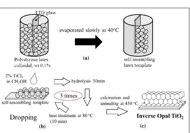
Figure 2.1 Schematic procedure of the fabrication inverse opal TiO2 (a)
template preparation, (b) filling the template with TiO2 (c)
calcination of template and annealing of TiO2.
31
Figure 2.2 Flowchart of chemical solution preparation for CdSe adsorption. 33
Figure 2.3 Drawing of SILAR deposition for CdSe. 34
Figure 2.4 Schematic of the SEM column which focuses the electrons emitted from a heated tungsten filament into a small nanometer sized spot.
35
viii
Figure 2.7 Schematic diagram of photoacoustic spectroscopy. 42
Figure 2.8 Typical PA spectrum of carbon black. 43
Figure 2.9 Incident photon to current efficiency measurement setup. 45
Figure 2.10 Typical Current-Voltage characteristic curve of solar. 46
Figure 2.11 Air mass (a) optical path length of sunlight through Earth’s
atmosphere (b) solar irradiance spectrum.
47
Figure 3.1 Scanning electron microscopy (SEM) image of (a) IO-TiO2 and
(b) NP-TiO2.
52
Figure 3.2 PA spectra of CdSe QDs adsorbed on (a) IO-TiO2 and (b)
NP-TiO2 electrodes with different numbers of CdSe SILAR cycles.
53
Figure 3.3 Tauc plots of CdSe QDs adsorbed on (a) IO-TiO2 and (b)
NP-TiO2.
55
Figure 3.4 Dependence of the average diameter of CdSe QDs adsorbed on IO-TiO2 and NP-TiO2 electrodes on the number of CdSe SILAR
cycles.
56
Figure 3.5 Dependence of width of the exponential tail of CdSe QDs adsorbed on IO-TiO2 and NP-TiO2 electrodes on the number of
SILAR cycles.
58
Figure 4.1 IPCE spectra of CdSe QDs adsorbed on IO-TiO2 (a) and NP-TiO2
(b) electrodes with different CdSe SILAR cycles.
69
Figure 4.2 J-V curves of CdSe QDSSCs with different CdSe SILAR cycles (a) IO-TiO2 (b) NP-TiO2.
70
Figure 4.3 Equivalent circuit of a solar cell. 72
Figure 4.4 Dependence of the Rsh (a) and Rs (b) on CdSe SILAR cycle. 74
ix SILAR cycles.
Figure A.3 Incident photon current efficiency spectra of PbS/CdS sensitized solar cell.
82
Figure A.4 Current density and voltage curve of PbS/CdS sensitized solar cell. 83
Figure A.5 Photovoltaic properties of PbS/CdS sensitized solar cell (a) Efficiency (b) Short circuit current density (c) Open circuit voltage (d) Fill factor
x
List of tables
Table 1.1 List of some properties of CdSe (Wurtzite structure). 19
Table 2.1 Rosencwaig-Gersho special case for thermally thick samples. 42
Table 4.1 Photovoltaic properties of CdSe QDs adsorbed on TiO2 electrodes
with different CdSe SILAR cycles.
75
Table A.1 Photovoltaic properties of PbS and CdS QDs adsorbed on TiO2
electrodes with different SILAR cycles.
1
Introduction
1.1 Introduction
1.1.1 Background
At the present time, most of the world’s consumption of energy is based on coal, oil and natural gas. However, the use of this fossil fuel could result in pollution. Burning coal produces sulphur dioxide, an acidic gas that contributes to the formation of acid rain and burning any fossil fuel produces carbon dioxide, which leads to the "greenhouse effect", warming the Earth.Greenhouse effects melt glaciers at the arctic regions and will cause not only an increase of sea level but also other atmospheric phenomena that could ultimately result in significant ecological problems for the earth. There has been an enormous increase in the demand for energy since the middle of the last century as a result of industrial development and population growth. In the 1970s, “Middle east oil crisis” panicked world due to petroleum shortage and high gasoline prices. The supply shortage and environmental problems have attracted our interest to find another energy source beyond fossil fuel. While there are already alternative energy sources, there are tradeoffs in the use of many of these sources. For example, nuclear power is a powerful and long-term alternative energy source but radioactive materials from nuclear power plants are extremely hazardous, and the disposal of the nuclear waste after power generation is a complicated environmental issue. These concerns became even more visible after the recent earthquake in Japan and the resulting tsunami crippled the nuclear
2
power plants. Radioactive materials from the reactor chambers contaminated not only the soil and sea water but also the Earth’s atmosphere. Nuclear energy, which was considered to be one of the best candidates as an alternative energy source, is now being reconsidered as a safe and stable energy source. Therefore, renewable energy sources which are generated from natural resources such as sunlight, wind, water, and so forth have emerged as clean alternative energy sources for the future. Solar energy is an alternative renewable energy without any environmental damage. The following is several advantages of solar energy,
Inexhaustible fuel source
No pollution (enviromentally friendly)
Readily availability (in a sunny enough climate)
Often an excellent supplement to other renewable sources
Versatile, is used for powering items as diverse as solar cars and satellites Therefore, a significant number of researchers have been focused on developing high efficiency, stable and low cost solar cells using various materials for a long time.
Photovoltaic effect
Photovoltaic effect is the basic process through which a solar cell converts solar radiation into electricity, which was first observed by Henri Becquerel [1] in 1839. He generated electricity between two electrodes attached to a liquid system upon irradiating light onto this system. The next significant photovoltaic development arose from the first demonstration of photovoltaic effects in selenium (solid-state system) by Adam and Day [2] in 1876. They observed the photovoltaic effect by illuminating a junction between the platinum and selenium. The next significant step forward came with the work of Fritts [3] in 1883. He was able to prepare a selenium solar cell, the first "thin-film" photovoltaic
3
devices, consisted of thin selenium films which adhered to one metal plate (e.g. brass) and gold leaf.
Fundamentally, there are three basic requirements for the photovoltaic effect (shown in Fig. 1.1). First, upon irradiation, light or photon should be absorbed creating electron-hole pairs. Then these electron-hole pairs should be separated so that their recombination is inhibited. In the end, these electrons and holes should be collected separately by each of collecting electrodes. Anode is the electrode collecting electrons and cathode is electrode collecting holes. Thus, current can be induced to flow in an external circuit.
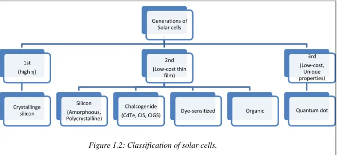
Classification of solar cells
Generally, solar cell technologies are classified into three generation (shown in Fig. 1.2) according to Martin Green from University of New South Wales (UNSW). The first generation solar cells is aimed to obtain high efficiency and mainly based on crystalline silicon, which is currently used worldwide with the best laboratory energy
n-type
p-type
-
+
external
load electron-hole pair
4
conversion efficiency achieved 25%. The theoretical limit of the solar cell using single junction is calculated by Shockley and Queisser [4] to be about 31%, limited to the thermalization loss of hot carriers (heat loss of the excess kinetic energy of hot photogenerated carriers created by the absorption of photon with high energy) and no absorption of photon with energy less than band gap. In fact to synthesis such high purity silicon, it requires high cost, energy-intensive high-temperature (more than 1000 OC) and high-vacuum processes. The cost of silicon solar cell may be reduced by thin film technology (known as second generation solar cells), in which thin film silicon solar cells are mainly deposited by chemical vapour deposition (CVD) from silane gas (SiH4) and
hydrogen in 200 OC. This process produces amorphous silicon (no crystalline orientation) with lower conversion efficiency. The best laboratory efficiencies could be achieved
20% for polycrystalline silicon and 15% for amorphous silicon. The other second generation solar cells include the chalcogenide material, such as cadmium telluride (CdTe), copper indium sulfide (CIS) and copper indium gallium selenide (CIGS). These materials are applied in a thin film to a supporting substrate such as glass or ceramics reducing material mass and therefore costs. These technologies, particularly CIGS-CIS, DSC and CdTe offer significantly cheaper production costs. Dye-sensitized solar cells (DSSCs) and organic solar cells are the advanced thin film photovoltaic with low cost and simple production based on photoelectrochemical method. So far, the energy conversion efficiency of DSSCs could exceed 11% [5]. Third generation solar cells aim to enhance the performance of second generation (thin-film technologies) while maintaining very low production costs. Current research purposes to obtain the energy conversion efficiencies of 30-60% while retaining low cost materials and manufacturing techniques. This may be achieved by exploiting the
5
hot photogenerated carriers in quantum dots (QD) to produce higher photovoltages or higher photocurrents. The former is based on miniband transport and collection of hot carriers in QD array photoelectrodes before their relaxation to the band edges through photon emission and heat loss consequently. The latter is based on generation and collection additional electron-hole pairs by utilizing hot carriers in QD solar cells through enhanced impact ionization processes. Further, the scope in this study concentrates on the DSSCs and the application of semiconductor QD (i.e. CdSe QD) as photosensitizer replacing dye.
Dye-sensitized solar cells (DSSCs)
Dye Sensitized TiO2 Nanocrystalline solar cells (DSSCs) has attracted much
attention becacuse they are generally made from inexpensive and nontoxic components, and can be designed in a diversity of colors and transparencies. Since the pioneering work of dye-sensitized nanocrystalline TiO2 by Grätzel and co-workers in 1991 [6], efforts
have been made to improve the performance of DSSCs. However, the development of DSSCs has been slow over the last ten years, with the highest record of 12% ever
Generations of Solar cells 1st (high η) Crystallinge silicon 2nd (Low-cost thin film) Silicon (Amorphoous, Polycrystalline) Chalcogenide
(CdTe, CIS, CIGS) Dye-sensitized Organic
3rd (Low-cost,
Unique properties)
Quantum dot
6
reported [7]. In this cell, the use of dye molecules as photosensitizers, nanostructured TiO2 as the electron transport layer and I¯/I3¯redox couple as hole transport layer
dramatically improve light harvesting efficiency. Based on the DSSC’s structure, quantum dot (QDs) was introduced as a replacement of dye to its excellent opto-electronic properties [8]. Quantum dot-sensitized solar cells (QDSSCs) are interesting photovoltaic devices because quantum dots show some benefits, such as quantum high extinction coefficient, quantum confinement effect and so on. Particularly, the multiple exciton generation (MEG) of QD solar cells can theoretically give about 44% of conversion efficiency, higher than Shockley–Queisser efficiency limit. Due to the quantum confinement effect, the bandgap of semiconductor nanoparticles and, hence its optical absorption, can be modulated over a wide spectral range by controlling their size to match the distribution of solar light. Moreover, semiconductor nanocrystals have robust inorganic nature so these particles are more stable against photodegradation than the usual organic dyes. With these advances, researchers were able to fabricate solar cell devices achieving efficiency up to 7% in QD related solar cells [9].
The relatively low efficiency obtained in DSSC is assigned to the poor penetration of material into the thick TiO2 film, and the detachment of hole transport layer from TiO2
electrode [10]. In order to address the penetration of both sensitizers and redox couples, a novel approach has been proposed using mesoporous inverse opal titania starting from self-organizing systems, such as opal of polystyrene latex, as template. This inverse opal (volumetric inverse of opal) titania has large interconnected pores lead to better infiltration. In addition, it also exhibits photonic band gap (frequency range that will not allow the propagation of particular wavelengths because of multiple Bragg reflection), which depends on the filling fraction of TiO2 in the inverse opal structure. On the
red-edge of the photonic band gap, the photon will be localized in high refractive index layer of sensitized inverse opal TiO2 thus could significantly enhance the sensitizer absorption,
7
especially in the edge of optical absorption where the sensitizer absorbs weakly solar light [2].
Quantum dot-sensitized solar cells (QDSSCs) may improve the efficiency by both materials development and the progress in understanding the cell mechanisms. Materials development involves (1) the emergence of absorber such as CdSe, CdS, PbS and Sb2S3,
which extend the light absorption range from the visible to the near-infrared region [11], (2) the improvement of QD synthesis and loading using successive ionic layer adsorption and reaction (SILAR) [12], chemical bath deposition (CBD) [13], monodisperse QDs with molecular linkers [14], and direct adsorption (DA) [15], (3) different morphology of wide metal oxide semiconductors [16], (4) new counter electrode [17], and (5) the improvement of redox couple electrolyte [18]. In addition, the basic understanding of the cell mechanisms includes (1) the existence of several electron injection paths [19], (2) fast hole extraction relative to electron recombination [20], (3) charge accumulation in QDs layer [21], (4) the effect of surface modifications of both the QDs and the metal oxide [22].
1.1.2 Purposes
Based on the background mentioned above, this study mainly focuses on the study and application of inverse opal structured electrode and CdSe QD replacing nanocrystalline electrode and dye sensitizer, respectively. CdSe is selected among the other semiconductors due to the possible electron injection from CdSe to TiO2 and its
well-known properties. The purposes of this study are as follows:
1. Synthesis of three dimensional inverse opal TiO2 and characterize its physical
properties.
2. Adsorbing of CdSe quantum dots on inverse opal TiO2 and characterize the
8
3. Investigation on the photovoltaic properties of CdSe QD-adsorbed inverse opal TiO2 and introduce suggestions for better solar cells.
1.1.3 Brief outline of the thesis
This thesis consists of a total of 5 chapters. The first chapter shows the introduction to this field, purpose and outline of this thesis. Moreover, it provides a general overview of some of the concepts that are needed for reading this thesis, such as background of TiO2 and related theories of semiconductor quantum dots. It is by no
means a complete overview, thus many references are necessary to provide the comprehensive background to this field.
Chapter 2 explains the experimental procedures, i.e. sample preparations and used characterization techniques. The former includes the inverse opal TiO2 preparation and
the method to adsorb the CdSe QD in situ on inverse opal TiO2. The latter includes the
used technique to characterize its structure, morphology, optical absorption, photocurrent, photovoltaic properties.
Chapter 3 shows the adsorption of CdSe in situ on inverse opal TiO2 and its effect
on the morphology. Photoabsorption of inverse opal TiO2 with CdSe QDs is studied by
characterizing its optical absorption by photoacoustic spectroscopy as a function of SILAR cycles. Moreover, size of semiconductor nanoparticle is calculated from the effective mass approximation. Urbach parameter is determined from the optical absorption band edge to consider defects of TiO2 adsorbed with CdSe QDs.
Chapter 4 contains characterization of the photovoltaic properties of CdSe QD-sensitized inverse opal TiO2 in solar cell application. The typical photovoltaic properties
will be compared with those of CdSe QD-sensitized nanoparticulate TiO2 solar cells.
9
electrolyte, usually used as redox couple in QD-sensitized solar cells. Further improvements are suggested resulting in efficient QD-sensitized solar cells.
Finally, chapter 5 summarizes the whole results in this study. In addition, an appendix is added in this thesis, which investigates co-sensitized solar cell. PbS/CdS quantum dot sensitized solar cell was studied by measuring optical absorption, photocurrent, and photovoltaic properties. The co-sensitized solar cell can have more conversion efficiency than solar cells with only single sensitizer.
1.2 Basics of TiO
21.2.1 Crystal Structural of TiO2
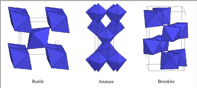
Titanium dioxide occurs in nature in three mineral forms: rutile, anatase and brookite, additionally two high pressure forms, the monoclinic baddeleyite form and the orthorhombic α-PbO2 form have been found at the Ries crater in Bavaria [23]. Rutile is
the most common form in nature and the most stable polymorph among the three modifications. Anatase and brookite both convert to rutile upon heating. Rutile, anatase and brookite all contain six coordinated titanium in the form of TiO6 octahedral, but with
different stacking-up topology. The crystal structures of the three polymorphs were illustrated in Fig. 1.3. Both rutile and anatase crystalize in tetragonal system. The two crystal structures differ in the distortion of each octahedron and by the assembly pattern of the octahedra chains. In rutile, the octahedron shows a slight orthorhombic distortion, while the octahedron of anatase is significantly distorted so that its symmetry is lower than orthorhombic. The name of anatase roots from the Greek “anatasis” which means
10
"extension", indicating the vertical axis of the crystals being longer than that in rutile [24]. Brookite crystallizes in the orthorhombic system. Brookite occurs rarely compared to the anatase and rutile forms of titanium dioxide. Because brookite shows no photocatalytic activity, it attracts the least research interest. These differences in lattice structures cause difference mass densities and electronic structures as well as other chemical and physical properties.
1.2.2 Applications of TiO2
TiO2 is one of the top fifty chemicals produced worldwide. Since its commercial
production in the early twentieth century, titanium dioxide has been widely used as a pigment in sunscreens, paints, ointments, toothpaste, etc. It provides for maximum whiteness and opacity [25]. It does so more effectively than any other white pigment. These unique properties are derived from the refractive index of titanium dioxide which is the highest among any material known to man, even greater than diamond.
Rutile Anatase Brookite
11
TiO2 is also a potent photocatalyst that can break down almost any organic
compound when exposed to sunlight [26]. A wide range of environmentally beneficial products utilizing TiO2's reactivity are being developed including self-cleaning fabrics,
auto body finishes, and ceramic tiles. Also in development is a paving stone that uses the catalytic properties of TiO2 to remove nitrogen oxide from the air, breaking it down into
more environmentally benign substances that can then be washed away by rainfall. It remains to be seen, however, whether the formation of undesirable intermediate products during these processes outweighs the benefits offered by TiO2's photocatalytic properties.
As the most promising photocatalyst, TiO2 materials are expected to play an
important role in helping solve many serious environmental and pollution challenges. The general scheme for the photocatalytic destruction of organic compounds involves the excitation of the semiconductor by irradiation with suprabandgap photons, and continues through surface redox reactions. One of the applications is photovoltaic application. Photovoltaics based on TiO2 nanocrystalline electrodes have been widely studied [27]. At
the heart of the system is a nanocrystalline mesoporous TiO2 film with a monolayer of the
charge transfer dye attached to its surface. The film is placed in contact with a redox electrolyte or an organic hole conductor. Photoexcitation of the dye injects an electron into the conduction band of TiO2. The electron can be conducted to the outer circuit to
drive the load and make electric power. The original state of the dye is subsequently restored by electron donation from the electrolyte, usually an organic solvent containing a redox system, such as the iodide/triiodide couple. The regeneration of the sensitizer by iodide prevents the recapture of the conduction band electron by the oxidized dye. The iodide is regenerated in turn by the reduction of triiodide at the counter electrode, with the circuit being completed via electron migration through the external load. The voltage generated under illumination corresponds to the difference between the Fermi level of TiO2 and the redox potential of the electrolyte. Overall, the device generates electric
12
1.2.3 TiO2 nanomaterials
When the dimension of matter is brought down to nanometer scale, many of its features would easily change and have many unique features both different from macro-matters and single atoms due to the quantum effect, regional confinement of matter, and ultra-high surface area or interface effects [28]. The final objective of nanotechnology is to produce products of special functions with new physical and chemical features by making atoms, molecules and matters presenting their features directly in the length of a nanometer such as: the strength of ten times of iron could be very light, all the information in a library could be stored in a chip the size of a sugar cube, and tumors the sizes of only several cells can be detected. Titanium dioxide's photocatalytic characteristics are greatly enhanced due to the advent of nanotechnology [29]. At the nano-scale, not only the surface area of titanium dioxide particle increases dramatically but also it exhibits other effects on optical properties and size quantization. An enhanced rate in photocatalytic reaction is observed as the redox potential increases and the size decreases [30]. The same effect also applies to the photovoltaic application, which also utilizes the photo-generated charge carriers. Due to its potent performance in photocatalysis and photovoltaic application, tremendous interests and efforts have been devoted to research on TiO2 nanomaterials in terms of synthesis and modification,
property characterization, fundamental mechanism investigation, theoretical calculation, and application. The TiO2 nanomaterials synthesis methods are summarized as a chart in
Fig. 1.4. The physical methods mainly include mechanical milling and physical vapor deposition. The chemical routes especially wet-chemibcal routes are extensively used to synthesize TiO2 materials. It can be further categorized into sol-gel,
13
hydrothermal/solvothermal, micelle/inverse micelle, sonochemical/microwave, and electrochemical techniques. These techniques are mainly based on the hydrolysis or solvolysis between titanium-containing precursors and the solvent or chelating agents with or without external assistance such as elevated temperature and pressure in hydrothermal reactor, surfactant in micelle method, microwave or sonar energy to facilitate or direct the crystal growth.
1.2.4 Template-based synthesis
In a general way, “template” is defined as a central structure within which a network forms in such a way that removal of the template creates a filled cavity with morphological and/or stereochemical features related to those of template. A method termed “template synthesis” entails the preparation of a variety of micro- and
Synthesis Method
Chemical
CVD, Direct
oxidation Wet chemical
Electrochemistry Sol-gel solvothermal Hydro/ Micelle and inverse micelle sonochemical Microwave/ Physical
Mechanical PVD
14
nanomaterials of a desired morphology and, therefore, provides a route for enhancing nanostructure order. Various porous “templates” are employed and the nanostructures are synthesized within the pores. If the templates used have spherical pores of uniform diameter, monodisperse nanospheres of the desired material are obtained within the voids of the template material. Depending on the operating parameters, these nanospheres may be solid (forms opals) or hollow (forms inverse opals). The nanostructures can remain inside the pores of the templates or they can be freed and collected by removing the templates. The most frequently used templates are polystyrene film. Two essential steps are needed. First step is to deposit the desired materials to fill the pores inside the membrane. Various deposition techniques could be utilized such as sol-gel, polymerization, atomic layer deposition (ALD), pulsed laser deposition (PLD), etc [31]. The second step is to remove the template to release and collect the nanostructures. Polystyrene can be removed by high temperature firing. Depending on the specific technology used, the process might have some additional steps involved. Various deposition techniques have been used to create titania 3-D structure inside the pores of template. Sol-gel is frequently used. The formula and recipe of sol-gel is not different from traditional sol-gel to produce nanoparticles or bulk materials. One just has to dip the template into the sol before the gelation happens to fill the pores with the sol under the drive of capillary force and gravity. Additional assistances could be taken to help the sol penetrate into the pores, such as centrifudge [32], vacuum pump [33], etc. One can also pre-treat the template surface to enhance the hydrophobicity or hydrophilicity depending on the sol formula to improve the filling efficiency. After filling, the sol-filled template will go through the same gelation-drycalcination process to form the desired crystal structure. It commonly occurs that thin films form on the top and bottom surfaces of membrane. Thus it is necessary to wipe away excessive sol on the surfaces or use mechanical polishing to thinning the calcined films after calcination. Then the template is removed to release the titania nanostructures. The morphology of the obtained materials
15
closely associated with the network geometry of the template used, and clusters or bundles of opals are normally seen. Sol-gel is the most accessible and economical method to produce nanomaterials. One can also use other techniques to do the deposition step such as electrophoresis deposition, atomic layer deposition, etc, depending on the available instruments and experimental conditions. Utilizing different deposition steps one has also to slightly adjust the specific steps in pre-deposition and template-removal processes.
1.3 Semiconductor quantum dots as solar cell sensitizers
Quantum dots are semiconducting materials which are synthesized in such a way that they are spherical in shape and have diameters at or below the materials’ characteristic exciton Bohr radius. The Bohr radius of a material, which is linearly dependent on the materials’ relative dielectric permittivity and inversely dependent on the materials’ reduced effective mass has units of length and is a physical representation of the natural separation between a Coulombically bound electron and hole (exciton) within a material, such as what is generated immediately after the absorption of a photon. In bulk (large crystal lattice) materials, the crystal lattice is much larger than the size of the exciton, allowing free and independent movement of the exciton about the lattice. However, in a quantum dot, the size of the lattice is at or below the materials’ exciton Bohr radius, which translates to a confinement of the electron-hole pair to a volume less than what it naturally wants to occupy. This “confinement effect” results in discrete energy levels (as opposed to a continuum of energy levels in a bulk sample) which exhibit particle-in-a-box like behavior [34]. Specifically, the stronger the confinement—the smaller the diameter of the quantum dot—the larger the bandgap of the material. In terms of implementation into solar cells as next generation sensitizers, quantum dots offer the use of multiple bandgaps from a single material simply by changing the size of that material.
16
Therefore, to achieve maximum efficiency, one simply needs to optimize the performance of a single quantum dot material, which would efficiently convert one region of the solar spectrum due to the use of a single bandgap. Once this is achieved, one could then efficiently capture another region of the spectrum by changing the bandgap of the material, which in quantum dots means only changing the materials’ size. Another advantage to using QDs as sensitizers in next generation solar cells is the wealth of attention which has been paid to popular QD materials in their non-quantized forms. For example, because of their absorption characteristics within the visible region of the solar spectrum, single crystal cadmium chalcogenides (CdX, X = S, Se, Te) were identified by many as an alternative to silicon in single crystal devices. As a result, much work was done by Bard [35], Hodes [36], and Wrighton [37], among others, in the 1970s and 1980s regarding morphological and electrolyte effects on performance and stability of CdS [38], CdSe [39], and CdTe [40] bulk photoanodes. As quantization effects became better understood and techniques were developed to synthesize and characterize cadmium chalcogenide materials which exhibit quantum confinement in the 1990s and beyond, the focus of these materials as sensitizers for next generation photovoltaics shifted sharply
Figure 1.5. Artistic depiction of the materials which make up a quantum dot sensitized solar cell.
17
from bulk macroscopic samples to ordered nanostructured crystallites [41].
Quantum Dot Sensitized Solar Cell Design. Figure 1.5 shows an artistic depiction of
the basic design of a quantum dot sensitized solar cell (QDSSC). The fundamental difference between a QDSSC and a dye sensitized solar cell is the material used to harvest the visible portion of the solar spectrum. The following paragraph discusses the necessary energetic considerations needed to assemble a functioning QDSSC. In order to successfully substitute the sensitizer in Grätzel cell (the dye) with a semiconducting quantum dot, one needs to consider the characteristic energetics of each cell component. It is easiest to understand the effect of energetics on cell voltage through an energy diagram. Figure 1.6 shows the energetics of the QD sensitizer, the TiO2 scaffold, the
electrolyte solution, along with the working and counter electrodes. Note that the position of the QDs’ and TiO2’s conduction and valence bands, along with the position of the
electrolyte oxidation potential are shown as relative as opposed to absolute positions which are arranged in a way that promotes cell operation. The phrase “electrons sink and holes float” can be an aid in diagrams such as Figure 1.6, which literally means that electrons are energetically drawn to change energy level as low (more negative, vacuum
Figure 1.6. A diagram of the energetics which drive electron and hole transport in a quantum dot sensitized solar cell.
18
scale) as possible, and holes to energy level as high (more positive, vacuum scale) as possible. In order for all of the reactions to take place as described above the two relative energy requirements must be met: the QD conduction band must lie above the TiO2
conduction band, and the electrolyte potential must lie between the QD valence band and the TiO2 conduction band. The maximum voltage is then defined as the energetic
difference between the TiO2 conduction band and the electrolyte oxidation potential,
Figure 1.6 [42].
Figure 1.7: Band edges position of several semiconductors in contact with aqueous electrolyte at pH 1. The energy scale is indicated in electron volts using either the normal hydrogen electrode (NHE) or the vacuum level as a
19
1.3.1 Cadmium selenide
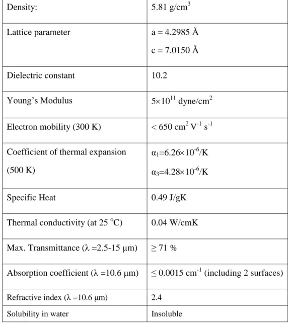
Cadmium selenide or cadmium (II) selenide, sometimes written as the chemical formula of CdSe, belongs to the class of II-IV semiconductors. CdSe is selected as the photosensitizer of TiO2 due to its smaller band gap of CdSe relative to TiO2 extending the
optical absorption to visible region as well as its well-known properties (shown in Table 1.1). Moreover, the more negative energetic bottom level in conduction band of CdSe
Table 1.1 List of some properties of CdSe (Wurtzite structure).
Density: 5.81 g/cm3
Lattice parameter a = 4.2985 Å
c = 7.0150 Å
Dielectric constant 10.2
Young’s Modulus 51011 dyne/cm2
Electron mobility (300 K) < 650 cm2 V-1 s-1
Coefficient of thermal expansion (500 K)
α1=6.2610-6/K
α3=4.2810-6/K
Specific Heat 0.49 J/gK
Thermal conductivity (at 25 oC) 0.04 W/cmK
Max. Transmittance (λ =2.5-15 μm) ≥ 71 %
Absorption coefficient (λ =10.6 μm) ≤ 0.0015 cm-1 (including 2 surfaces)
Refractive index (λ =10.6 μm) 2.4
20
than that of TiO2 and the more positive energetic top level in valence band of CdSe than
that of TiO2 (shown in Fig. 1.7 [43]) indicate the possible injection of photoexcited
electrons from CdSe to TiO2 conduction band and no injection of photoexcited holes
from CdSe to TiO2 valence band making the charge separation upon photoexcitation in
CdSe feasible.
CdSe is generally yellow to red crystalline solid with melting point at 1268°C. This material can be crystallized in either the wurtzite or hexagonal structure, as shown in Fig. 1.8. The formula weight is 191.37 g/mol. It is an intrinsic semiconductor with a band gap of 1.70 eV at 300 K. Some characteristics of CdSe in wurtzite structure are presented in Table 1.1.
In nano size, CdSe exhibits the quantum confinement effect where CdSe nanocrystals of different sizes exhibit different colors. With decreasing crystal size the band gap of the crystal increases and the dot emits more energetic or bluer photons. CdSe QDs which is grown by using method of colloidal chemistry, (core-shell) CdSe/ZnS with trioctylphosphine oxide (TOPO) as surface stabilizing molecule has high luminescence efficiency (65 %) at room temperature. Recently this nanocrystal has found important applications in Biology. QDs are coupled to biological molecules for use in ultrasensitive biological detection at the single-dot level. Quantum dots are used there as fluorescent tags capable of tracing specific proteins within cells and in the future it is hoped to develop lighting up DNA or viruses by QDs.
1.3.2 Quantum confinement effect
The band gap (Eg) of a semiconductor is defined as the energy difference between
the highest energy valence band states and the lowest energy conduction band states. The excitation of an electron from the valence band to the conduction band leaves a hole in the valance band. The electron and hole can form a bound state through Coulombic interactions. This bound electron-hole pair is called an exciton [44] (in this case a
21
Wannier exciton). The bound state has energy slightly less than the energy of the band gap.
When the radius of the nanoparticle approaches the size of the exciton Bohr radius, the motion of the electrons and holes become confined in the nanoparticle. The Bohr radius (aB) of the exciton is given by
* * 2 0 2 0 1 1 4 h e B m m e m a (2.1)
where is the high frequency relative dielectric constant of the medium me is the effective mass of the electron (in m0 units)
mh is the effective mass of the hole(in m0 units)
m0 is the mass of the electron at rest.
This resulting Bohr radius for excitons in semiconductors is much larger than that of hydrogen atom. A created electron-hole pair can only “fit” into a nanoparticle when the
Figure1.8: Solid state structure of CdSe. (a) Wurtzite structure (b) hexagonal structure.
Cd
Se
(a)
22
charge carriers are in a state of higher energy. As a consequence of this, the band gap increases with decreasing particle size. In this regime of spatial confinement, the kinetic energy becomes quantized and the energy bands split into discrete levels shown in Fig. 2.3. Regarding this, both the absorption and emission spectra of the material shift to higher energies with decreasing particle size.
One possible way to explain the quantum confinement effect is through the use of the effective mass approximation approach (EMA) [45]. Here, the size dependency of the band gap of the nanoparticle can be derived as:
R e m m R m E E o h e o g 4 8 . 1 1 1 2 2 * * 2 2 2 (2.2)
where R is the radius of the semiconductor particle and Eg is the band gap of the bulk
semiconductor. The first term in the equation above represents the particle in box
23
quantum localization energy and has a 1/R2 dependence. The second term represents the Coulomb energy having a 1/R dependence. For large R values, E approaches Eg.
1.3.3 Hot carrier and multiple exciton generation
Photoexcitation of a semiconductor with photons having energies above the band gap of semiconductor creates electron and holes with a total excess kinetic energy equal to the difference between the photon energy and band gap. This excess kinetic energy causes the effective temperature of carriers much higher than the lattice temperature, called as hot electrons and hot holes. To enhance the energy conversion efficiency, two fundamental ways to utilize hot carriers has been proposed by Nozik [46], i.e. enhanced photovoltage and enhanced photocurrent. By utilizing hot photogenerated carriers to produce higher photovoltages and photocurrents, the maximum attainable thermodynamic conversion efficiency of solar photon could increase up to about 66 % from 31% for Schokley-Queissar limit [47] of single band gap cells. The former requires the extraction of the hot carriers before they cool through their respective carrier-carrier collisions (called carrier thermalization) and carrier-phonon interactions (phonon emission occurs as the result of the cooling of the carriers and heating of the lattice until carrier and lattice temperatures become equal; the phonons involved in the process are the longitudinal optical phonons). In order to achieve this, the rates of the photogenerated carrier separation, transport and interfacial transfer across the semiconductor interface must all be fast compared with the rate of carrier cooling. The latter requires the energetic hot carriers to produce a second or more electron-hole pairs (multiple exciton generation, MEG) through impact ionization due to strong carrier-carrier interactions, as shown in Fig. 1.10. This is the inverse of an Auger process whereby two electron-hole pairs recombine to produce a single highly energetic electron-hole pair. Thus for enhanced photocurrent, the rate of impact ionization (i.e. inverse Auger effect) should be greater than the rate of Auger process or carrier cooling.
24
In bulk semiconductor, this MEG is inefficient because of the relatively weak Coulomb interactions, the restrictions imposed by energy and translational momentum conservation, as well as fast energy loss due to phonon emission. Strict selection rules and competing processes in the bulk permit MEG at energies of n x Eg where Eg is the
band gap of bulk semiconductorand n 3; however, efficient MEG is observed only for n
5 as a matter of fact [48]. On the other hand, MEG become efficient in zero-dimensional quantum dots with the lower values of n (typically 2 -3) [49] with respect to E1 (first excitation energy and not Eg any longer in quantum confinement regime) because
of wide separation between discrete electronic states inhibiting phonon emission due to phonon bottleneck, stronger Coulomb interactions and relaxation in translational momentum conservation. In phonon bottleneck [50], a large population of hot carriers produces a no equilibrium distribution of phonon (in particular, LO phonon that are the type involved in the electron-phonon interactions at high carrier energies) because the LO phonons cannot equilibrate fast enough with crystal bath; these hot LO phonons can be reabsorbed by the electron plasma to keep it hot. Besides Auger mechanism; electron-hole scattering, deep-level trapping and acoustical-optical photon interactions are other possible mechanisms for breaking the phonon bottleneck.
The first experimental evidence for high efficiency MEG in quantum dot was detected in PbSe QDs [51]. Later, MEG was also observed for QDs of other semiconductor, such as PbTe [52], CdSe [53], InAs [54] including an important photovoltaic material Si. Moreover, MEG in photocurrent was indicated in PbSe QD device structure. However, more recent studies have questioned the efficiency of MEG particularly for CdSe and InAs QDs. Synthesis differences between samples may left some with the QD surfaces that affect the efficiency of MEG. So engineering QDs is the key factor to optimize the potential MEG in solar cell applications.
25
Figure1.10: Representation of multiple exciton generation (E1 relating to
first excitation energy in quantum dot, likewise Eg relating to energy band gap of bulk semiconductor).
−
−
E
1+
−
−
−
+
+
+
hυ
nE
1−
− −
−
−
+ + + +26 _____________________
References
[1] A. Goetzberger, and V. U. Hoffman, Photovoltaic Solar Energy Generation (Springer, Germany, 2005).
[2] S. Nishimura, N. Abrams, B. A. Lewis, L. I. Halaoui, T. E. Mallouk, K. D.
Benkstein, J. van de Lagemaat, and A. J. Frank, J. Am. Chem. Soc. 125, 6306 (2003). [3] C. L. Huisman, J. Schoonman, and A. Goossens, Sol. Energy Mater. Sol. Cells. 85,
115 (2005).
[4] P. R. Somani, C. Dionigi, M. Murgia, D. Palles, P. Nozar, and G. Ruani, Sol. Energy
Mater. Sol. Cells 87, 513 (2005).
[5] W. W. Yu, L. Qu, W. Guo, and X. Peng, Chem. Mater. 15, 2854 (2003). [6] B. O'Regan, and M. Gratzel, Nature 353, 737 (1991).
[7] A. Yella, H. W. Lee, H. N. Tsao, C. Yi, A. K. Chandiran, M. K. Nazeeruddin, E. W. Diau, C. Yeh, S. M. Zakeeruddin, and M. Gratzel, Science 334, 629 (2011).
[8] R. Vogel, P. Hoyer, and H. Weller, J. Phys. Chem. 98, 3183 (1994).
[9] J. H. Im, C. R. Lee, J. W. Lee, S. W. Park, and N. G. Park, Nanoscale 3, 4088 (2011).
[10] S. Tanaka, Jpn. J. Appl. Phys. 40, 97 (2001). [11] J. P. Holdren, Science 456, 424 (2008).
[12] Y. L. Lee, and Y. S. Lo, Adv. Funct. Mater. 19, 604 (2009).
[13] S. J. Roh, R. S. Mane, S. K. Min, W. J. Lee, and S. H. Lokhande, Appl. Phys. Lett.
89, 253512 (2006).
[14] J. Chen, J. L. Song, X. W. Sun, W. Q. Deng, C. Y. Jiang, W. Lei, J. H. Huang, and R. S. Liu, Appl. Phys. Lett. 94, 153115 (2009).
27
[15] S. Giménez, I. Mora-Seró, L. Macor, N. Guijarro, T. Lana-Villarreal, R. Gómez, L. J. Diguna, Q. Shen, T. Toyoda, and J. Bisquert, Nanotechnology 20, 295204 (2009). [16] J. Xu, X. Yang, Q. Yang, T. Wong, S. Lee, W. Zhang, and C. Lee, J. Mater. Chem.
22, 13374 (2012).
[17] J. Kim, H. Choi, C. Nahm, C. Kim, S. Nam, S. Kang, D. Jung, J. I. Kim, J. Kang, and B. Park, J. Power Sources 220, 108 (2012).
[18] R. J. Ellingson, M. C. Beard, J. C. Johnson, P. Yu, O. I. Micic, A. J. Nozik, A. Shabaev, and A. L. Efros, Nano Lett. 5, 865 (2005).
[19] S. Ito, P. Liska, P. Comte, R. Charvet, P. Pechy, U. Bach, L. Schmidt-Mende, S. M. Zakeeruddin, A. Kay, M. K. Nazeeruddin, and M. Gratzel, Chem. Commun., 4351 (2005).
[20] Y. Liu, X. Sun, Q. Tai, H. Hu, B. Chen, N. Huang, B. Sebo, and X. Zhao, J. Power
Sources 196, 475 (2011).
[21] H. Choi, C. Nahm, J. Kim, J. Moon, S. Nam, C. Kim, D. Jung, and B. Park, Curr.
Appl. Phys. 12, 737 (2012).
[22] S. Waita, B. Aduda, J. Mwabora, G. Niklasson, C. Granqvist, and G. Boschloo, J.
Electroanal. Chem. 637, 79 (2009).
[23] A. E. Goresy, M. Chen, L. Dubrovinsky, P. Gillet, and G. Graup, Science 293, 1467 (2001).
[24] O. Carp, C. L. Huisman, and A. Reller, Progress in Solid State Chemistry 32, 33 (2004).
[25] G. Praff, and P. Reynders, P. Chem. Rev. 99, 1963 (1999).
[26] W. Plieth, Electrochemistry for Materials Science (Elsevier, 2008). [27] M. Gratzel, Nature 414, 338 (2001).
28 Scientific Publishers, 2004).
[29] X. Chen, and S. S. Mao, Chem. Rev. 107, 2891 (2007).
[30] M. R. Hoffmann, S. T. Martin, W. Choi, and D. W. Bahnemann, Chem. Rev. 95, 69 (1995).
[31] M. S. Sander, M. J. Cote, W. Gu, B. M. Kile, and C. P. Tripp, Adv. Mater. 16, 2052 (2004).
[32] T. Wen, J. Zhang, T. P. Chou, S. J. Limmer, and G. Cao, J. Sol-Gel Sci. Tech. 33, 193 (2005).
[33] J. Wang, A. Manivannan, and N. Q. Wu, Thin Solid Films 517, 582 (2008). [34] O. Millo, D. Katz, Y. W. Cao, and U. Banin, Phys. Rev. Lett. 86, 5751 (2001). [35] A. J. Bard, H. D. Abruna, C. E. Chidsey, L. R. Faulkner, S. D. Feldberg, K. Itaya, M.
Majda, O. Melroy, R. W. Murray, M. D. Porter, M. P. Soriaga, and H. S. White, J.
Phys. Chem. 97, 7147 (1993).
[36] J. Manassen, D. Cahen, G. Hodes, and A. Sofer, Nature 263, 97 (1976). [37] M. S. Wrighton, ACS Symp. Ser. 211, 59 (1983).
[38] C. Y. Liu, and A. J. Bard, J. Phys. Chem. 93, 7749 (1989).
[39] J. J. Hickman, and M. S. Wrighton, J. Am. Chem. Soc. 113, 4440 (1991). [40] K. D. Dobson, I. Visoly-Fisher, G. Hodes, and D. Cahen, Adv. Mater. 13, 1495
(2001).
[41] G. Hodes, and M. Gratzel, Nouv. J. Chim. 8, 509 (1984).
[42] D. Cahen, G. Hodes, M. Gratzel, J. F. Guillemoles, and I. Riess, J. Phys. Chem. B
104, 2053 (2000).
[43] A. Hagfeldt, and M. Gratzel, Chem. Rev. 95, 49 (1995).
29 York, 1986).
[45] L. E. Brus, J. Chem. Phys. 80, 4403 (1984).
[46] A. J. Nozik, Annu. Rev. Rhys. Chem. 52, 193 (2001).
[47] W. Shockley, and H. J. Queisser, J. Appl. Phys. 32, 510 (1961).
[48] S. Kolodinski, J. H. Werner, T. Wittchen, and H. Queisser, Appl. Phys. Lett. 63, 2405 (1993).
[49] A. J. Nozik, Physica E 14, 115 (2002).
[50] R. P. Joshi, and D. K. Ferry, Phys. Rev. B 39, 1180 (1989).
[51] R. D. Schaller, and V. I. Klimov, Phys. Rev. Lett. 92, 186601 (2004).
[52] J. E. Murphy, M. C. Beard, A. G. Norman, S. P. Ahrenkiel, J. C. Johnson, P. Yu, O. I. Micic, R. J. Ellingson, and A. J. Nozik, J. Am. Chem. Soc. 128, 3241 (2006). [53] R. D. Schaller, M. A. Petruska, and V. I. Klimov, Appl. Phys. Lett. 87, 253102
(2005).
30
Experimental procedures
2.1 Sample preparation
2.1.1 Inverse opal titanium dioxide
The inverse opal TiO2 was prepared by filling the void in an artificial template
and subsequently removing the template. Generally speaking, it can be grouped into three steps as follows, as briefly described in Fig. 2.1
(1) Template preparation [1]
1. Conductive fluorine-doped tin oxide (FTO) coated glass of 4.5 cm length and 2.3 cm width was cleaned ultrasonically with detergent, concentrated KOH, distilled water and methanol, consecutively.
2. 10 wt% of monodisperse hydrophobic polystyrene latex from Seradyn Co. was diluted with distillated water to a concentration of 0.1 wt%. The suspension was then dispersed ultrasonically for 30 min.
3. The FTO glass was immersed vertically in 30 ml beaker containing 15 ml latex suspension.
4. The beaker was then kept in an oven at 40°C for 1 to 2 days until the suspension was fully evaporated.
31
(2) Filling the void in template with TiO2
1. 2 % TiCl4 (from WAKO, 99 %) in methanol (from WAKO, 99.8 %) as
TiO2 source was prepared by mixing 2 ml TiCl4 and 98 ml methanol [2].
2. 2 % TiCl4 in methanol was vertically dropped on to a 1.3 x 2.3 cm
template by using a 10-μl sized micropipette.
3. The template was then kept in a desiccator (humidity 45-50 %, temperature 24-25%) for 30 min.
4. The template was heated in an oven at 80°C for 10 min. 5. The 2-4 processes were repeated for few times.
Figure 2.1: Schematic procedure of the fabrication inverse opal TiO2 (a) template
preparation, (b) filling the template with TiO2 (c) calcination of template and
annealing of TiO2.
(a)
32
In this step, heat treatment time at 80°C is necessary to make a compact structure before the further addition of TiCl4.
(3) Calcinations of the template and annealing of TiO2
Calcinations of the template and annealing of TiO2 were conducted together in
which the sample was heated at 450°C with 0.5°C/min heating rate. After 1 hour heating at 450°C, the temperature was cooled down to room temperature within 3 hours.
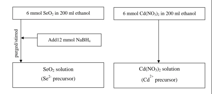
2.1.2 Adsorption of CdSe QDs on inverse opal TiO2
Figure 2.2 shows a flowchart of chemical solution preparation for CdSe adsorption and figure 2.3 shows the order of TiO2 is dipped in the solution. All chemicals
used in this deposition process are cadmium nitrate tetrahydrate (≥ 99.0 %), selenium dioxide (≥ 97.0%), and sodium tetrahydroborate (≥ 95.0%) obtained from WAKO. For this study, CdSe QDs adsorption on inverse opal TiO2 was conducted by successive ionic
layer adsorption and reaction (SILAR) method similar to what H. Lee, et. al. [3] has done. The adsorption procedure is as follows:
1. Weigh metal nitrates in vials in order to make 30 mM Cd(NO3)2 solution
later and put those inside the glove box.
2. 0.6657 g of SeO2 is dissolved in 200 mL ethanol (30 mM), and
purged/stirred for about 2 minutes and 0.4539 g of NaBH4 (60 mM) added
into the round-bottom flask containing SeO2, and purged/stirred for about
1 hour.
3. Pure ethanol in large volume is also prepared and purged for 1 hour separately for making metal nitrate solutions and washing the electrodes used inside glove box.
33
4. Move the bottom in (2) and (3) inside the glove box, which then was sealed and purged with inert gas (N2). Evacuation/purging were made the
inside atmosphere with a low oxygen level.
5 Inside the glove box, prepare metal nitrate solution designated above in one beaker and selenide solution in another beaker.
6. The TiO2-modified electrode was dipped into the metal2+ solution, pure
ethanol (then dried), the Se2- solution, and then pure ethanol (then dried) successively for 30 seconds for deposition each and longer time for washing and dried. Such an immersion cycle was repeated several times. The electrode became darker as the number of SILAR cycles was
increased.
6 mmol SeO2 in 200 ml ethanol
Add12 mmol NaBH4
SeO2 solution
(Se2- precursor)
Figure 2.2: Flowchart of chemical solution preparation for CdSe adsorption.
pur ged /s ti rr ed
6 mmol Cd(NO3)2 in 200 ml ethanol
Cd(NO3)2 solution
34
2.2 Characterization
2.2.1 Scanning electron microscopy [4]
Scanning electron microscopy (SEM) is the best known and most widely-used of the surface analytical techniques. The first Scanning Electron Microscope (SEM) debuted in 1942 with the first commercial instruments around 1965. SEM is considered a relatively rapid, inexpensive, and basically non-destructive approach to surface analysis. High resolution images of surface topography, with excellent depth of field are produced using a highly-focused, scanning (primary) electron beam. The primary electrons enter a surface with energy of 0.5 - 30 keV is focused in the microscope column (Fig. 2.4) though a combination of condenser lenses and apertures, and generate many low energy secondary electrons. The intensity of these secondary electrons is largely governed by the surface topography of the sample. An image of the sample surface can thus be constructed by measuring secondary electron intensity as a function of the position of the scanning primary electron beam. High spatial resolution is possible because the primary electron beam can be focused to a very small spot (< 10 nm). High sensitivity to topographic features on the outermost surface (< 5 nm) is achieved when using a primary electron beam with an energy of > 1 keV. In addition to low energy secondary electrons,