Annual Report of Hydrogen Isotope Research Center, University of Toyama, JAPAN
VOL 32 2012
富山大学水素同位体科学研究センター
研 究 報 告
第
32
巻2012
富山大学水素同位体科学研究センター
総 説
微粒子表面修飾・改質プロセスへのプラズマ技術の
適用と機能性微粒子材料の創成 ……… 阿 部 孝 之 …… 1
論 文
照射損傷を受けたタングステン中の重水素滞留挙
動に及ぼす Pd 表面被覆の影響 ………
V. Kh. Alimov
波多野 雄 治 杉 山 一 慶 高 木 郁 二 松 山 政 夫…… 9
多角バレルスパッタリング法を用いた固体高分子
形燃料電池用カソード触媒の劣化現象評価 ………
奥 島 康 正 井 上 光 浩 阿 部 孝 之
…… 21
湿潤空気下で保管した Li2+xTiO3+y の加熱に伴う重
量変化 ………
原 正 憲 水 内 理恵子 宮 尾 晃 司 松 山 政 夫 平 田 暁 子 大 矢 恭 久 奥 野 健 二
…… 27
ノート
繰り返し使用した
MCM-41
からのトリチウム水の脱着 ………
田 口 明 鳥 養 祐 二 松 山 政 夫
…… 35
交流磁束計を用いた
Pd
水素化物の電気抵抗測定 ………赤 丸 悟 士 原 正 憲 松 山 政 夫
…… 45
Review
T. ABE
Application of plasma technologies to particle surface treatment systems
and preparation of functionalized particle material
………1
Original
V. KH. ALIMOV, Y. HATANO, K. SUGIYAMA, I. TAKAGI. M. MATSUYAMA
Deuterium Retention in Self-Damaged Tungsten with and without Deposited Pd Layer
……9
Y. OKUSHIMA, M. INOUE, T. ABE
Degradation of Cathode Catalysts for Polymer Electrolyte Fuel Cells Studied
Using the Polygonal Barrel-Sputtering Method
………21
M. HARA, R. MIZUUCHI, K. MIYAO, M. MATSUYAMA, A. HIRATA, Y. OYA, K. OKUNO
Weight change of Li
2+xTiO
3+yStored in Moist Air by Heating
………27
Note
A. TAGUCHI, Y. TORIKAI, M. MATSUYAMA
Desorption of tritiated water from reused MCM-41
………35
S. AKAMARU, M. HARA, M. MATSUYAMA
Measurement of Electrical Resistivity of Pd hydride
by using Alternating-Current Magnetometer
………45
総 説
微粒子表面修飾・改質プロセスへのプラズマ技術の適用と 機能性微粒子材料の創成
阿部 孝之
富山大学水素同位体科学研究センター
〒930-8555 富山市五福 3190
Application of plasma technologies to particle surface treatment systems and preparation of functionalized particle materials
Takayuki Abe
Hydrogen isotope research center, University of Toyama Gofuku 3190, Toyama 930-8555, Japan
(Received February 22, 2013; accepted April 19, 2013) Abstract
Particle surface modification of powdered materials has currently attracted considerable attention in various industrial and scientific fields. However, conventional wet processes, such as plating and impregnation method, produce wastewater streams containing potentially harmful residual chemicals. In addition, the wet processes involve the decomposition of precursors by heating and chemical reduction, which interfere with controlled surface modification. To avoid such drawbacks of wet processes, we have developed novel particle surface modification methods based on the plasma technologies. In our original surface modification methods, a polygonal barrel containing the powdered sample is rotated or oscillated to stir the particles during treatment, achieving the uniform modification of the particle surfaces. Since plasma technologies used in our methods are categorized as dry processes, they do not accompany wastewater discharge. Furthermore, the treatment in our methods is carried out without heating or chemical reduction, allowing controlled surface modification. This report describes the particle surface modification using the
“polygonal barrel-sputtering method”, “polygonal barrel-plasma chemical vapor deposition method”, and
“polygonal barrel-plasma treatment method”.
「微粒子材料の機能化」は種々の産業において欠かせない技術である。また最近の生産活動は、
環境に配慮した経済活動の重要性の高まりにより「大量生産・消費型」から「環境に配慮した省 エネ型」にシフトしつつある。この観点からも、微粒子材料の機能化とその性能の向上(高機能・
高性能微粒子材料の開発)は省エネ型産業を成し遂げる上で重要である。しかし近年、微粒子材 料の機能化に対する要求は多種多様化しており、もはやバルク材の材料開発だけでは、その要求 に答えることは難しい。そのため、「微粒子材料の表面修飾・改質」が注目されており、この手 法による高機能材料の創成が多くの科学・産業分野で期待されている。
化学反応は一般的に材料の「表面」で進行する。それ故、反応の高効率化を計る上で、材料表 面の修飾や改質は極めて有効な手段であることが半経験的に知られている。しかし、取り扱う材 料が「微粒子」の場合、巨視的に見れば「0次元体」であるが、微視的には「3次元体」と言える 特異な形状特性のため、微粒子の表面の修飾や改質は容易ではない。例えば微粒子表面にある種 の物質を修飾する場合、めっき法[1,2]や含浸法[3-5]等に代表される「ウェットプロセス」が用い られるが、このプロセスでは修飾物質の前駆体(錯体等)の還元過程(加熱、あるいは化学還元)
が必須であり、修飾物質の厳密な制御(表面デザイン)は極めて難しい。また、プロセス中で用 いられる溶液(強酸、強アルカリ)や添加剤(シアン、発がん性有機物)等の破棄も環境負荷の 観点から大きな問題となっているだけでなく、これら有害物質の処理は水質汚濁防止法・土壌汚 染対策法や種々の都道府県条例により厳しく規制されており、ウェットプロセスによる事業拡大 や新規参入は非常に困難な状況になっている。
これに対し、有害物質を使用せず、排液処理も不要なドライプロセスによる表面修飾法は非常 に魅力的である。プラズマ技術を基にしたスパッタリング法[6]やプラズマ化学蒸着(PCVD)法[7]
は代表的な乾式表面修飾法である。しかし、これらの表面修飾法は高い指向性を有するためコン パクトディスク等の平板(疑似的
2
次元)材料表面へのナノレベル修飾技術としては優れている が、微粒子(0 次元、3次元)材料表面への修飾法としては不向きであった。
そこで我々は、プラズマ技術を基にした新たな 三次元材料表面修飾法を独自に開発した。その一 例として図
1
に「多角バレルスパッタリング法」を示す[8-22]。この方法の特徴はスパッタリング 時に微粒子を入れた多角バレル(容器)を回転、
あるいは振り子動作させることで微粒子を効率 的に撹拌し、微粒子表面の均一修飾が可能なこと である。また、修飾物として種々の材料(金属・
合金・金属酸化物等)を選択できるとともに、担 体として用いられる微粒子材料のサイズや材質 の制限もない。さらに前述したウェットプロセス での「前駆体の使用」や「還元過程」もないこと
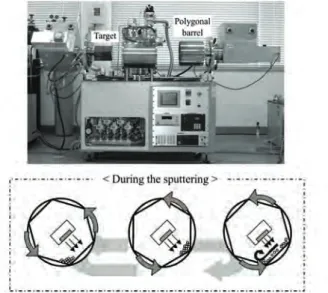
Figure 1 A photograph of the polygonal
barrel-sputtering system and a schematic
とともに、微粒子表面をナノレベルでデザインする ことが可能となった。最近ではスパッタリング法の 代わりに
PCVD
法を用いた「多角バレルPCVD
法」[23]や微粒子表面層をナノレベルで改質(新規物質
層の構築)可能な「多角バレルプラズマ微粒子表面 改質法」[24,25]も新たに開発している。ここでは、これら手法を用いた微粒子表面修飾・改質の一例と 創成した微粒子材料の機能性について紹介する。
2.
多角バレルスパッタリング法による微粒子表面 修飾[8-22]2.1
金属皮膜の修飾[8-10]まず、多角バレルスパッタリング法による微粒子 材料の表面修飾について記す。図
2(I)には Pt
を修飾 したポリメタクリル酸メチル(PMMA)微粒子(粒 径: 50 μm)の光学顕微鏡写真を示している[9]。修飾 前のPMMA
微粒子は白色であるのに対し、Pt スパ ッタリング後は金属色を呈している。また個々の微 粒子表面には隣接する微粒子からの反射光が映り 込むほど、光沢のある鏡面になっていることが見て取れる。これらの結果は、多角バレルスパッタリング法により、
PMMA
微粒子表面がPt
薄膜(TEM 観察より、膜厚約50 nm)で均一にコーティングされていることを明示している。図 2(II)には他
の金属薄膜を修飾したPMMA
微粒子(粒径: 15 μm)の写真を示した[10]。それぞれの試料は、修 飾した金属に由来する色を呈している。また図2(III)に示す SEM
像では粒子表面の形態には大き な違いは認められないが、EPMA
像ではSEM
像と同じ形状で各種元素が一様に検出された。すな わち、多角バレルスパッタリング法による均一な薄膜コーティングは金属種に依存しない。なお、多角バレルスパッタリング法では用いる担体に制限がなく、例えば岩塩のような水溶性 微粒子表面にも均一修飾が可能であること、またボルト・ナット・ネジのような複雑な形状を有す る
3
次元材料でも表面を均一に金属コーティングでき[16]、「めっき」の代替となるドライプロセス としても有望であることも明らかとしている。2.2
化合物薄膜の修飾[11-15]多角バレルスパッタリング法は、反応性スパッタリングにより微粒子表面に種々の化合物薄膜 も修飾できる。一例として、SnO2を修飾したアルミフレークの写真を図
3(I)に示した[11]。試料
の色は調製時のRF
出力増加(0、195、350、490 W)に従って、金属色(アルミ自体の色)から 黄→赤→青と変化した。それぞれの試料が単一の干渉色を呈していることは、個々のアルミフレFigure 2 (I) Optical microscope images of
PMMA particles (particle size: 50 μm) before
and after Pt film-coating. (II) Photographs
and (III) SEM and EPMA images of PMMA
powder samples (particle size: 15μm) coated
with various metal films.
かつ一つの微粒子表面においても膜厚にムラがな いことを示している。実際に試料の断面
SEM
像(図
3(II))には均一な厚みの SnO
2膜が認められ、その薄膜は微粒子表面の凹凸に沿って形成されて
いた(図
3(II-A)白円内参照)。また、これらの SEM
像から膜厚は
195 W: 80±15 nm、 350 W: 130±20 nm、
490 W: 180±20 nm
と見積もられ、図3(I)に示す試
料の色相変化がSnO
2 膜厚の増加に伴う干渉色変 化に起因していることが明らかとなった。なお、紙面の関係上割愛するが、他の酸化物(TiO2、
WO
3)[12,13]、炭化物(WC)[14]、窒化物(TiN)[15]
による微粒子表面修飾についても報告している。
2.3
カーボンナノチューブ・ナノファイバー(1次元)材料の表面修飾[17]カーボンナノチューブ(CNT)やカーボンナノファイバー(CNF)は、ナノメートルオーダー の繊維径を持つ一次元の炭素材料であり、特異な電気伝導性や機械的強度を有することから、幅 広い分野で注目されている。例えば、金属ナノ粒子を担持した
CNT
やCNF
は燃料電池用電極触 媒やバイオセンサーなどへの応用が検討されている。しかし、通常のウェットプロセスを用いたCNT
やCNF
表面への金属ナノ粒子担持には、1)CNTおよびCNF
表面の前処理が必要、2)金属
ナノ粒子のチューブ内析出が避けられない、などの問題が指摘されている。そこで、多角バレル スパッタリング法を用いて、未処理のCNT
および
CNF
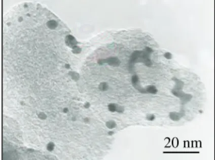
表面への金属ナノ粒子修飾を試みた。図4(A)には繊維径 150 nm(繊維長: 10~20 μm)の CNF
にPt
を担持した試料のTEM
像を示した。比較のために、担持前の
CNF
表面も図4(B)に示
した。修飾前のCNF
表面は比較的平坦であるの に対し、修飾後の試料表面には黒い点として見える粒径
2~4 nm
のPt
ナノ粒子(平均粒径: 2.2nm)が極めて均一に担持されていることがわか
る。同様な結果はCNT(繊維径: 10 nm、繊維長:
5~15 μm)でも得られている。次に、試料台を
種々の角度に傾けながら随時
TEM
測定を行った。図
4(C)は含浸法で調製した試料の結果である。
(i)で示した Pt
ナノ粒子(粒径: 8 nm)は試料台の角度変化に追随して徐々に図中下側に移動した が、(ii)の粒子は全く移動していない。つまり、
Figure 4 TEM images of (A) Pt-deposited CNF and (B) as-received CNF. (C) and (D) show the TEM images of Pt-deposited CNF samples prepared by an impregnation method and the polygonal barrel-sputtering method, respectively,
After Before
Average 2.2 nm
(A) (B)
(C)
(D) (ii)
(i)
(iii)
Figure 3 (I) A photograph of Al flakes before and after SnO
2-film coating. (II) Cross-sectional SEM images of the Al flakes coated with SnO
2films (AC power, A: 195, B: 350, C: 490 W).
まで達することがわかった。一方、多角バレルスパッタリング法で作製した試料(図
4(D))では、
(iii)で示したナノ粒子のように全粒子の移動が認められた。すなわち、担持した Pt
ナノ粒子は全て
CNF
外表面に均一に担持されていることを示している。2.4
機能性微粒子の作製[18-22]ここまで微粒子の均一表面修飾について記してきたが、ここからは多角バレルスパッタリング 法で調製した機能性微粒子材料(例として「触媒」)について述べる。一般に、「触媒」は特異な機 能(活性化エネルギーの低減や選択性の向上など)を発現する各種工業・産業における影の立役者 である。従来、不均一触媒は含浸法のようなウェットプロセスを用いて調製されていたため、ブ ラックボックス的な要素が多く含まれていた。すなわち、溶媒、錯体、添加物などが存在する環 境下において、これらの物質やイオンが最終生成物に与える影響はほとんど考慮されていない。
また、さまざまな前処理や後処理なる工程(表面処理、加熱還元、酸化処理など)も必要である。
これでは「デザインされた触媒表面」を構築し、目的とする化学反応を制御することは至難の業で ある。一方、我々が開発した多角バレルスパッタリング法は種々の調製要素を制御しやすいドラ イプロセスであり、上記問題を排除した触媒調製が可能である。以下では近年、世界中で問題視 されている二酸化炭素(CO2)の削減に寄与する高性能触媒について記す。
2.4.1
燃料電池用電極触媒の調製[18-21]最近、CO2排出量削減に有効な発電システムである固体高分子型燃料電池(PEFC)が自動車や 家庭用電源として実験的な使用が開始されている。しかし、本格的な実用化を目指すためには、
更なる耐久性向上やコスト削減が不可欠である。幾つもの要素技術の革新的なブレークスルーが 必要であるが、電極材料として用いられている
Pt
やPt
合金の使用量削減や電極自体の高性能化も その一つである。著者らは多角バレルスパッタリング法を用いてカーボン担体上にPt-Ru
合金を 担持したアノード触媒(Pt-Ru/C、合金組成: Pt:Ru=50:50 at.%)を調製し、その特性を検討した[18,19]。その結果、図
5
に示すように、本法で調製した試料のPt-Ru
合金ナノ粒子は、市販触媒より明ら かに微細で粒径も均一であった。また、調製試料に担持された個々のナノ粒子の合金組成は52.9:47.1 (±5.3) at.%
で あ り 、 市 販 触 媒 の 組 成(51.0:49.0~89.4:10.6 at.%)に比べ、極めて均一 であった。さらに、調製した試料の
CO
耐性や水 素酸化特性も市販品に比べ優れていることを明 らかにした[18]。これらの特性により、調製試料 をアノードに用いた場合、発電性能を低下させ ることなく金属使用量を普及時の目標レベル(現状の約
1/10
以下)にまで削減できることを 示した[18]。なお、本法を用いた直接メタノール 燃料電池用電極触媒[20,21]の電気化学特性につFigure 5 TEM images of Pt-Ru/C anode catalysts
for PEFCs with data of atomic ratios (Pt:Ru) of
individual alloy particles.
2.4.2 CO
2メタン化触媒の調製[22]不均一触媒を用いた
CO
2水素化によるメタン生成 反応(CO2+4H
2→CH
4+2H
2O)は CO
2削減に対し有効 であるだけでなく、生成したメタンを燃料として再 利用できる利点を有する。しかし、この触媒反応は通常
400℃程度の熱を必要とし(新たな CO
2発生誘引)、今まで「意味のない反応」と考えられてきた。
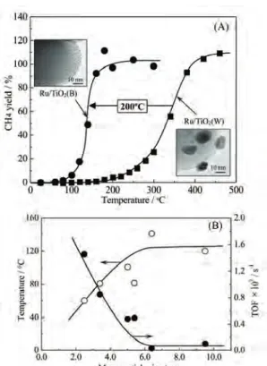
しかし最近、多角バレルスパッタリング法を用いて
TiO
2 微 粒 子 上 にRu
ナ ノ 金 属 を 担 持 し た 触 媒(Ru/TiO2
(B))では室温から CO
2の水素化反応が進行し、約
150℃で転化率、選択率共に 100%の触媒活
性を示すことを見出した(図
6(A)参照)[22]。これ
は 含 侵 法 で 調 製 し た 従 来 のRu
担 持 触 媒(Ru/TiO2
(W))に比べ、 200℃以上低温で反応が進行
することを示している。両者の触媒物性を比較したところ、
Ru/TiO
2(B)では担持された Ru
粒子の粒径が約
2~3 nm
であり、かつ粒径分布も単分散系に近いことがわかった。一方、焼成・還元処理が必要な
Ru/TiO
2(W)の Ru
粒径分布は5~20 nm
であり、Ru/TiO
2(B)と明らかに異なっていた。さらに Ru
粒子径とTON
数(表面積を考慮した反応速度)、および反応開始温度の詳細な検討から、Ru粒子径が
6 nm
以下になるとTON
数が急激に増加し、それにともない反応開始温度も低下することが明らかとなった(図
6(B))。つまり、Ru/TiO
2(B)
触媒の高い活性は担持金属の高表面積化に依存しているのではなく、担持金属粒子のナノ化によ る特異な物性変化に起因していることが示唆された。この結果は、Ru/TiO2(B)を用いた CO
2メタ ン化反応がCO
2削減に貢献できる「極めて有望な反応」であることを示している。実用化の第一歩 として、現在、この触媒を利用した宇宙ステーションでのCO
2(主に呼吸)除去に関する研究を 宇宙航空研究開発機構(JAXA)と実施している。3.
多角バレルPCVD
法による微粒子表面修飾[23]上記した多角バレルスパッタリング法は微粒子表面修飾法として優れているが、修飾する物質
(カーボンや酸化物等)によっては、長時間の作業(修飾)時間を必要とする(物質のスパッタ リング速度に依存)。この問題を解決するため、スパッタリング法の代わりに
PCVD
法を用いた。PCVD
はガス状前駆体物質(カーボン修飾の場合、各種炭化水素)をプラズマ分解し、微粒子表 面に目的物質を高速コーティングできる。また、本法は加熱が不要であることから、微粒子材料 として耐熱性の低いポリマー等も使用できる。近年、PCVD 法はハードディスク材の表面やペッFigure 6 (A) Temperature dependence of the
methane yield at methanation of CO
2over
Ru/TiO
2samples. Insets show TEM images
of Ru/TiO
2(B) and Ru/TiO
2(W). (B) Plots of
the onset temperature of methane formation
and TON at 160ºC versus and the mean
particle size of Ru on TiO
2.
をコーティングする手法として広く用いられているが[7]、
ここでは新たに開発した「多角バレル
PCVD
法」を用い て、PMMA微粒子(粒径: 50 μm)表面のDLC
薄膜のコー ティングを試みた。処理前後の試料の外観写真と光学顕 微鏡写真を図7(I)、 (II)に示す(A:
処理前、B:
処理後)[23]。
処理前の白色の外観(粒子は半透明)は、
PCVD
処理によ りすべての粒子が茶褐色に変化した。物性評価から、こ の茶褐色への色相変化はDLC
膜の均一修飾に起因するこ とがわかった。なお、DLC 膜厚は処理時間とともに増加 し、その結果、試料の色相は濃くなった。また、処理試料は
30%硝酸中に 3
日間浸漬しても全く変化(溶解等)せず、化学的安定性も向上した。
4.
多角バレル微粒子表面改質法による微粒子表面処理[24,25]
ここまで述べてきた「多角バレルスパッタリング法」・「多角バレルプラズマ
PCVD
法」は、微粒子表面に物質(金属・酸化物・カーボン等)を均一に修飾する手法であった。これに対し、
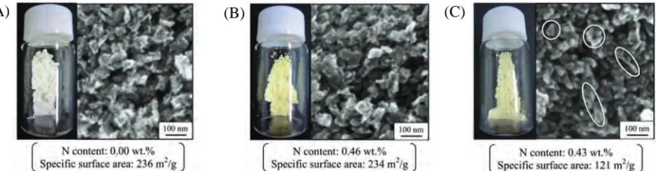
民間企業と共同で新しく開発した「多角バレルプラズマ微粒子表面改質法」は微粒子表面そのも のをナノスケールで改質する手法である。ここでは一例として、光触媒として良く知られる
TiO
2微粒子(平均粒子径: 7 nm)の窒化処理前後の写真と
SEM
像を図8(A)、(B)に示した[24]。参考の
ために、アンモニア雰囲気で550℃加熱処理して調製した試料写真も図 8(C)に載せている。いず
れの処理法でも試料は白色から黄色に変化した。また、N含有量は約0.45 wt.%に増加し、各種物
性評価から、TiO
2表面での窒素ドープが明らかとなった。しかしSEM
像から、プラズマ処理試料 の粒子は処理前と違いがないのに対し、加熱処理試料では粒子の融着が認められた(図8(C)白円
内)。これらの窒素ドープ粒子の変化は、加熱処理試料の比表面積が処理前の1/2
程度にまで減 少したのに対し、多角プラズマ微粒子表面改質法では比表面積が処理前と同等であるという違い に現れた。つまり本法はマイルドな条件で微粒子表面を改質できる画期的な手法である。(A) (B) (C)
Figure 8 Photographs and SEM images of (A) as-received TiO
2sample, (B) plasma-treated TiO
2sample, and (C) NH
3-treated TiO
2sample with data of N contents and specific surface areas.
Figure 7 (I) Photographs of (A) untreated and (B) treated PMMA powder samples in a glass bottle and (II) optical microscope images of the obtained particles.
(A)
(B)
今回紹介した「多角バレルスパッタリング法」・「多角バレル
PCVD
法」・「多角バレルプラ ズマ微粒子表面改質法」は環境に優しい微粒子表面修飾・改質法であり、従来法で成し得なかっ た「微粒子表面をナノレベルでデザインする」画期的な技術である。これらの手法による表面修 飾は機能性ナノ材料の開発をブレークスルーする可能性を秘めており、さまざまな分野への応用 展開も期待できる。References
(1)
星野重夫, 表面技術, 56 (2005) 302.(2)
稲本順一, 表面技術, 57 (2006) 889.(3) T. Kawaguchi, W. Sugimoto, Y. Murakami and Y. Takasu, Electrochem. Commun., 6 (2004) 480.
(4) Y. Suwa, S. Ito, S. Kameoka, K. Tomishige and K. Kunimori, Appl. Catal. A: Gen., 267 (2004) 9.
(5) C. Bock, B. MacDougall and Y. LePage, J. Electrochem. Soc., 151 (2004) A1269.
(6)
金原粲, スパタリング現象 基礎と薄膜・コーティング技術への応用,(東京大学出版, 1984)(7) C. Casiraghi, J. Robertson and A.C. Ferrari, Mater. Today, 10 (2007) 44.
(8) T. Abe, S. Akamaru and K. Watanabe, J. Alloys Compd., 377 (2004) 194.
(9) T. Abe, S. Akamaru, K. Watanabe and Y. Honda, J. Alloys Compd., 402 (2005) 227.
(10) A. Taguchi, T. Kitami, H. Yamamoto, S. Akamaru, M. Hara and T. Abe, J. Alloys Compd., 441 (2007) 162.
(11) T. Abe, S. Higashide, M. Inoue and S. Akamaru, Plasma. Chem. Plasma, Process., 27 (2007) 799.
(12) S. Akamaru, S. Higashide, M. Hara and T. Abe, Thin Solid Films, 513 (2006) 103.
(13) T. Abe, H. Hamatani, S. Higashide, M. Hara and S. Akamaru, J. Alloys Compd., 441 (2007) 157.
(14) S. Akamaru, H. Yamamoto and T. Abe, Vacuum, 83 (2009) 633.
(15) S. Akamaru, Y. Honda, A. Taguchi and T. Abe, Materials Transactions, 49 (2008) 1638.
(16) A. Taguchi, T. Kitami, S. Akamaru and T. Abe, Surf. Coat. Technol., 201 (2007) 9512.
(17) H. Yamamoto, K. Hirakawa and T. Abe, Mater. Lett., 62 (2008) 2118.
(18) M. Inoue, H. Shingen, T. Kitami, S. Akamaru, A. Taguchi, Y. Kawamoto, A. Tada, K. Ohtawa, K.
Ohba, M. Matsuyama, K. Watanabe, I. Tsubone and T. Abe, J. Phys. Chem. C, 112 (2008) 1479.
(19) M. Inoue, S. Akamaru, A. Taguchi and T. Abe, Vacuum, 83 (2009) 658.
(20) K. Hirakawa, M. Inoue and T. Abe, Electrochim. Acta, 55 (2010) 5874.
(21) C. Hiromi, M. Inoue, A. Taguchi and T. Abe, Electrochim. Acta, 56 (2011) 8438.
(22) T. Abe, M. Tanizawa, K. Watanabe and A. Taguchi, Energy Environ. Sci., 2 (2009) 315.
(23) Y. Honda, S. Akamaru, M. Inoue and T. Abe, Chem. Eng. J., 209 (2012) 616.
(24) K. Matsubara, M. Danno, M. Inoue, Y. Honda and T. Abe, Chem. Eng. J., 181–182 (2012) 754.
(25) K. Matsubara, M. Danno, M. Inoue, Y. Honda, N. Yoshida and T. Abe, Phys. Chem. Chem. Phys., 15
(2013) 5097.
照射損傷を受けたタングステン中の重水素滞留挙動に及ぼす Pd 表面被覆の影響
Vladimir Kh. Alimov
1,
波多野雄治1,
杉山一慶2,
高木郁二3,
松山政夫11富山大学水素同位体科学研究センター
〒930-8555 富山市五福
3190
2
Max-Planck-Institut für Plasmaphysik, EURATOM Association, D-85748 Garching, Germany
3京都大学大学院工学研究科原子核工学専攻
〒606-8501 京都市左京区吉田本町
Deuterium Retention in Self-Damaged Tungsten with and without Deposited Pd Layer
Vladimir Kh. Alimov
1, Yuji Hatano
1, Kazuyoshi Sugiyama
2, Ikuji Takagi
3, Masao Matsuyama
11
Hydrogen Isotope Research Center, University of Toyama, Toyama 930-8555, Japan
2
Max-Planck-Institut für Plasmaphysik, EURATOM Association, D-85748 Garching, Germany
3
Department of Nuclear Engineering, Kyoto University Kyoto 606-8501, Japan
(Received January 31, 2013; accepted May 7, 2013) Abstract
Influence of Pd deposition on deuterium (D) retention in W samples irradiated
with W self-ions was examined to understand the correlation between the probability of
occupation of radiation-induced traps by D and the concentration of D in a solid
solution state under plasma exposure. W samples were irradiated with 4.8 MeV W ions
to 0.65 and 12 dpa, and a thin Pd layer was deposited on the sample with the higher damage level by a technique of sputter-deposition. Then, the samples were exposed to DC glow-discharge D plasma at 403 K. In spite of the higher damage level, the concentration of trapped D in the damaged zone of the Pd-covered sample was far smaller than that in the non-covered one. The small D retention in the Pd-covered sample was explained by a decrease in the D concentration in the solution state owing to the enhanced recombinative release by Pd and the consequent reduction in the occupation probability of radiation-induced traps. These observations indicated that tritium inventory in neutron-irradiated W materials can be significantly reduced by enhancement of tritium reemission by surface modifications.
1. Introduction
Tungsten (W) and its alloys are recognized as candidates of plasma-facing materials of future fusion reactors. Because defects such as vacancies and voids act as strong traps for hydrogen isotopes, tritium (T) inventory in neutron-irradiated W materials is an important problem in safety assessment of fusion reactors. Indeed, significant increase in deuterium (D) retention in W after neutron irradiation in a fission reactor was reported in Refs. [1–6]. It is also known that irradiation effects by neutrons can be simulated by irradiation with high energy ions [7].
Under exposure to hydrogen isotope plasma, a majority of hydrogen particles
impinging on the W surface are emitted back to the plasma through recombination into
molecules on the surface and subsequent desorption. A minor portion of impinging
hydrogen isotopes settles in interstitial sites in the bcc lattice, diffuses in the lattice, and
then gets trapped when they encounter unoccupied defects. Under exposure to high flux
plasma, formation of bubbles and blisters takes place in the near-surface regions by precipitation of molecular hydrogen isotopes in cavities. The hydrogen isotope retention in blisters and bubbles increases practically infinitely with increase in internal pressure, and these defects can be called as unsaturable traps. On the other hand, in the bulk of materials where chemical potential is far lower, hydrogen isotopes are trapped in atomic form in defects such as dislocations, vacancies, and vacancies clusters with finite capacity. These defects are often referred as saturable traps. In this study, the attention is focused on the trapping effects in the bulk of materials, and hence only saturable traps are considered below. Inventory of hydrogen isotopes increases with increase in the fraction of occupied traps. Based on the model proposed by Beshers [8], the fraction of occupied traps
tat temperature T is expressed as
t,i/(1 −
t,i) =
Lexp(E
bin,i/kT), (1) where
Lis the fraction of occupied interstitial sites, E
bin,iis the binding energy between hydrogen isotope and defect, i is the type of defect and k is the Boltzmann constant.
This equation suggests that the fraction of occupied trap sites and consequently inventory of hydrogen isotopes increases with an increase in the concentration of hydrogen isotopes in the solid solution state C
SSbecause C
SSis proportional to
L. Even under the conditions where E
bin,i/kT >> 1 (i.e.
t≈ 1), the inventory of hydrogen isotopes depends on C
SSif a discharge pulses are short enough to keep the penetration depth of hydrogen isotopes smaller than the thickness of W materials [9]. If E
bin,i/kT >> 1, clear interface between filled zone (
t≈ 1) and empty zone (
t≈ 0) can be observed, and the velocity of the interface is
dx/dt = D
LC
SS-S/xN
t, (2)
where x is the depth from the surface, t is time, D
Lis the diffusion coefficient of hydrogen isotopes in the lattice of W, and N
tis the trap density [10]. Here, C
SS-Sis the concentration of hydrogen isotopes in the solution state just beneath the plasma-facing surface. Although C
SSincluding C
SS-Sis far smaller than the concentration of trapped hydrogen isotopes, the variation in C
SShas strong influence on total inventory of hydrogen isotopes. Indeed, such correlation between C
SSand inventory of D was demonstrated by a gas absorption technique under equilibrium conditions in our previous papers [5,11]; C
SSwas determined as a function of pressure of D
2gas and temperature. However, the correlation under non-equilibrium conditions, such as under plasma exposure, has not been proven.
The objective of the present study is to demonstrate the effects of surface modification of W on D inventory in MeV-range W-ion-irradiated W. A thin Pd layer was prepared on the surface of the W-ion-irradiated W sample, and then the samples with and without Pd layers were exposed to weakly-ionized D plasma created by DC glow discharge. Weakly-ionized plasma is suitable to examine the interaction between hydrogen isotopes and saturable traps because such low-flux plasma does not form blisters. As previously reported [11], the W-ion-induced defects in the sample without Pd layer become fully occupied during plasma exposure of surface to a depth depending on implantation fluence (or time) and are empty at greater depths; the D depth profiles are consistent with saturable traps being filled by D atoms diffusing from the surface.
The mass balance at the plasma-facing surface can be expressed as
in= k
rC
SS-S2where
is the sticking coefficient of impinging particles,
inis incident flux and k
ris the
surface recombination rate constant. Hence, C
SS-S= (
in/k
r)
1/2. Although k
rfor a clean
W surface is very high (k
r≥10
−11m
4s
−1at ≤ 1000 K [7]), such surface state is available
only in an ultra-high vacuum. The values of k
rreported for W with ion-implantation [12] and linear plasma machines [5] are just k
r≥ 10
−20m
4s
−1owing to contamination by impurities such as oxygen and carbon. On the other hand, Pd is a noble metal and its surface is less sensitive to contamination by impurities. In addition, solubility of hydrogen isotopes in Pd is significantly larger than that in W, and Pd overlayers would provide high C
SS-Stogether with low C
SSin the W substrate.
2. Experimental
Polycrystalline mechanically-deformed W from A.L.M.T. Co., Japan, with a purity of 99.99 mass%, was used in this work. Two W disc-type samples, 6 mm in diameter and 0.2 mm in thickness, were prepared by cutting a polycrystalline tungsten rod annealed at 1173 K for 3.6 ks in a hydrogen atmosphere to relieve internal stresses occurred in the manufacturing process. The samples were mechanically polished to a mirror finish with diamond powders (9- and 3-m-sized grains) and colloidal silica suspension (40-nm-sized grains). After cleaning in an ultra-sonic bath with acetone, surfactant and de-ionized water for 5 min each, the samples were annealed at 1173 K for 1.8 ks in vacuum (∼10
−6Pa). The grains are elongated along the direction normal to the surface, which is similar to ITER-grade W.
The first W sample (sample #1) was irradiated with 4.8 MeV W ions at
temperature of 573 K to damage levels of 0.65 displacements per atom (dpa) at the
damage peak, whereas the second sample (sample #2) was irradiated with 4.8 MeV W
ions at 300 K to 12 dpa. The damage profiles were calculated using the program SRIM
2008.03 [13], “full cascade option”, with the displacement energy of E
d= 90 eV as the
more reliable value for the W lattice [14,15]. Note that for irradiation with 4.8 MeV W
ions, the damage peak situated at a depth of 0.23 µm.
The damaged sides of sample #1 were exposed to D plasma formed by DC glow discharge at temperature of 403 K [11]. The sample was set on a holder equipped with an ohmic heater and a thermocouple served as anode, whereas W disc located at a distance of about 10 cm from the sample holder was used as a cathode. Deuterium pressure in the chamber was maintained at 1 Pa, DC discharge voltage was 400 V, and discharge current averaged about 0.18 A. Because the sample was set on an anode, the main impinging particles are D atoms and molecules (D neutrals) in addition to electrons. The energies of atoms were in the range from few eV (atoms originated in the glow discharge) to ~150 eV (atoms reflected from the W cathode). The flux of implanted deuterium was estimated to be about 210
18D/m
2s with the use of Ti probe exposed in the DC glow discharge at 300 K for 10 and 60 min, while the D retention in the Ti probe was determined by thermal desorption spectroscopy [11]. The implantation fluence was about 610
22D m
−2.
Sample #2 was exposed to the D plasma in a similar manner at 403 K to the implantation fluence of about 610
22D/m
2, but with Pd cathode instead of W one.
Owing to far larger sputtering yield for Pd than W by 400 eV D ions, the surface of
sample #2 was covered by sputtered Pd particles. Here, the sputtering yield for W is
3×10
−3[16]. The sputtering yield for Pd is not available, but that for Ag locating next to
Pd in the periodic table is 0.1 [16]. Thickness of the deposited Pd layer on the sample
was determined by means of Rutherford backscattering spectroscopy (RBS) at
3He ion
energies of 2.8 MeV and evaluated with SIMNRA program [17]. The backscattered
3He
was energy-analyzed at a scattering angle of 165° by a small-angle surface barrier
detector. It was found that after D plasma exposure for 30 ks (that corresponded to the
1600 0 2000 2400 4000
8000
Counts
Energy (keV) RBS, 165
0Detector
Analysing beam: 2.8 MeV
3He
+W
RBS experimental data simulation with SIMNRA 58 nm Pd layer on W
RBS experimental data simulation with SIMNRA
Fig. 1 Rutherford backscattering (RBS) spectra for 2.8 MeV
3He ions incident on tungsten with and without 58 nm thick Pd layer deposited on the W surface. The symbols and solid lines represent respectively experimentally measured and calculated RBS spectra. The RBS spectra were calculated by the SIMNRA program [17].
implantation fluence of about 610
22D/m
2), a thickness of Pd layer was around 270 nm.
After the RBS measurement, the Pd layer on sample #2 was thinned by sputtering with Ar ions in a commercial glow-discharge optical emission spectroscopy (GDOES) device (Horiba Jobin Yvon, GD-Profiler 2). Repeated RBS measurement performed after that showed that a thickness of the Pd layer was reduced to 58 nm (Fig. 1). Sample
#2 with 58 nm Pd layer was exposed to the D plasma with the use of the W cathode at
403 K to the implantation fluence of about 610
22D/m
2. Namely, sample #2 was
sequentially exposed to D plasma 2 times with the in-situ Pd deposition up to 270 nm
and with the pre-prepared thin Pd layer (58 nm).
The deuterium profiles in samples #1 and #2 after exposure to the D plasma were determined by nuclear reaction analysis (NRA) at IPP, Garching. The D(
3He,p)
4He reaction was utilized, and both the particles and protons were analyzed. To determine the D concentration at larger depths, an analyzing beam of
3He ions with energies varied from 0.69 to 4.0 MeV was used. The proton yields measured at different
3He ion energies allow measuring the D depth profile at depths of up to 6 μm.
3. Results and discussion
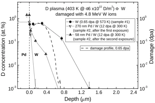
Generation of displacement damage in the sample #1 at 573 K and subsequent exposure to D plasma at temperature of 403 K leads to accumulation of deuterium at depths up to 2 µm (i.e., in the damage zone) to concentrations of about 0.6 at.% as shown in Fig. 2. Note that after exposure to D
2gas at pressure of 1 Pa (the same deuterium pressure was maintained under DC glow discharge) and temperature of 403 K for 30 ks (i.e., for time period of the D fluence), the D concentration in the damage zone does not exceed 10
−3at.%. It should be noted that, in undamaged W exposed to the D plasma, the D concentration at depths 0.1 µm is below the NRA detection limit of 510
−4at.%.
In the sample #2 exposed to the D plasma with the Pd cathode, deuterium is accumulated mainly in the 270 nm thick Pd layer (Fig. 2). However, after thinning of the Pd layer to 58 nm and second D plasma exposure with the W cathode, the D concentration in the W damage zone is significantly lower than that for the W sample
#1 without Pd film (Fig. 2), in spite of higher defect concentration. Note that in the
sample #2 irradiated with 4.8 MeV W ions at 300 K to the damage level of 12 dpa, a
0.0 0.4 0.8 1.2 1.6 2.0 2.4 10
-310
-210
-110
010
-310
-210
-110
0Damage (dpa)
D conc entration (at.%)
Depth ( m)
W (0.65 dpa @ 573 K) (sample #1) 270 nm Pd / W (12 dpa @ 300 K) (sample #2, after the first exposure)
58 nm Pd / W (12 dpa @ 300 K) (sample #2, after the second exposure)
D plasma (403 K @ 6 x10
22D/m
2) W damaged with 4.8 MeV W ions
damage profile, 0.65 dpa
Pd W
Fig. 2 Depth profiles of D retained in the sample #1 and sample #2 after the first and second D plasma exposures. Thickness of the Pd layer on the sample #2 after the first and second D plasma exposures is indicated in the legend. A boundary between the Pd layer and the W substrate corresponds to a depth of 0 µm. Damage profile is plotted in a logarithmic scale on the right ordinate axis.
concentration of defects responsible for trapping of diffusing D atoms is slightly higher than that for W-ion irradiation at 573 K to 0.65 dpa [5].
Obviously, the deposited Pd film on the W surface serves as a storage for implanted D and reduces flux of diffusing D atoms penetrating into the damage zone by increasing k
rC
SS-S2. Note that the diffusivity of D in Pd is 4.5 × 10
−10m
2s
−1at 403 K [18].
Hence, the mean diffusion length of D during the exposure to D plasma for 30 ks is
evaluated to be 5 mm. This value of mean diffusion length is far larger than the
thickness of Pd layer (58 nm). It means that the low concentration of trapped D in W
damage zone in sample #2 was not owing to slow diffusion in the Pd layer. The D
concentration in sample #2 beneath the surface (Pd region) was ca. 1 at.% (6.9 × 10
26D m
−3). Since
inunder exposure to D plasma was about 210
18D m
−2s
−1, the k
rwas evaluated to be 4 × 10
−36m
4s
−1. This value is in reasonable agreement with that reported by Pick and Sonnenberg [19]. The entropy and enthalpy of H solution in Pd are
−60 J mol
−1K
−1and −10 kJ mol
−1, respectively [18]. Hence, the above-mentioned D concentration (1 at.% at 403 K) corresponds to equilibrium pressure of 31 kPa. On the other hand, the concentration of D in a solid solution state in W at this pressure (31 kPa) and temperature (403 K) can be evaluated from the solubility data reported by Frauenfelder [20] to be 2.5 × 10
13D m
−3(3.9 × 10
−16in [D]/[W]). According to Eq. (1), at this fraction of occupied interstitial sites,
L, the fraction of occupied traps,
t, becomes equal to or below 0.1 if E
bin≤ 1.2 eV. Since the activation energy for diffusion of H in W is 0.39 eV, this E
bincorresponds to the activation energy for desorption of ca.
1.6 eV. This means that occupation probability of mono-vacancies [21] and dislocations [22] by D is negligibly small. Namely, low concentration of trapped D in sample #2 can be explained by low occupation probability of defects with small E
binowing to low D concentration in the solid solution state. In other words, under plasma exposure, the retention of hydrogen isotopes in irradiated W can be reduced by reduction in the D concentration in the solid solution state by enhancement of recombinative release.
4. Summary
Preparation of a Pd layer on an MeV-range W-ion-irradiated W sample resulted
in significant reduction in D retention after exposure to DC glow-discharge D plasma at
403 K. The reduced D retention was explained by decrease in D concentration in a solid
solution state caused by enhancement of recombinative D release by the Pd layer and
consequent reduction in occupation probability of radiation-induced traps. These observations indicated that tritium inventory in neutron-irradiated W materials can be significantly reduced by enhancement of tritium reemission by surface modifications.
References
[1] M. Shimada et al., J. Nucl. Mater. 415 (2011) S667.
[4][2] M. Shimada et al., Phys. Scr. T145 (2011) 0014051.
[6][3] Y. Oya et al., Phys. Scr. T145 (2011) 0014050.
[7][4] M. Shimada et al., Fusion Eng. Des. 87 (2012) 1166.
[8][5] Y. Hatano et al., Trapping of hydrogen isotopes in radiation defects formed in W by neutron and ion irradiations, J. Nucl. Mater. (2013),
http://dx.doi.org/10.1016/j.jnucmat.2013.01.018.
[6] Y. Hatano et al., Retention of hydrogen isotopes in neutron irradiated tungsten, Mater. Trans. 54 (2013) 437.
[7] J. Roth and K. Schmid, Phys. Scr. T145 (2011) 0014031 and references therein.
[8] D. N. Beshers, Acta Metall. 6 (1958) 521.
[9] D. G. Whyte, J. Nucl. Mater. 390-391 (2009) 911.
[10] W. R. Wampler, R. P. Doerner, Nucl. Fusion 49 (2009) 115023.
[11] V. Kh. Alimov, Y. Hatano, K. Sugiyama, J. Roth, B. Tyburska-Püschel, J. Dorner, J. Shi, M. Matsuyama, J. Nucl. Mater. (2013),
http://dx.doi.org/10.1016/j.jnucmat.2013.01.208.
[12] R.A. Anderl, D.F. Holland, G.R. Longhurst, R.J. Pawelko, C.L. Trybus,
[13] J.F. Ziegler, SRIM - The Stopping and Range of Ions in Matter, ver.
SRIM-2008.3, available on http://srim.org.
[14] Standard Practice for Neutron Radiation Damage Simulation by Charge-Particle Irradiation, E521-96, Annual Book of ASTM Standards, Vol. 12.02, American Society for Testing and Materials, Philadelphia, 1996, p. 1.
[15] Q. Xu, T. Yoshiie, H.C. Huang, Nucl. Instr. Meth. B 206 (2003) 123.
[16] H.H. Andersen and H.L. Bay, Chapter 4 Sputtering Yield Measurements, in Sputtering by Particle Bombardment I, Ed. by R. Behrisch, Springer-Verlag
Berlin Heidelberg, 1981.
[17] M. Mayer, SIMNRA User’s Guide, Tech. Rep. IPP 9/113, Garching, 1997.
[18] Y. Fukai, The Metal-Hydrogen System Basic Bulk Properties , Springer-Verlag Berlin Heidelberg, Germany, 2005, pp. 14–27.
[19] M. A. Pick and K. Sonnenberg, J. Nucl. Mater. 131 (1985) 208.
[20] R. Frauenfelder, J. Vac. Sci. Technol. 6 (1969) 388.
[21] H. Eleveld and A. van Veen, J. Nucl. Mater. 212-215 (1994) 1421.
[22] O.V. Ogorodnikova, B. Tyburska, V. Kh. Alimov and K. Ertl, J. Nucl. Mater. 415
(2011) S661.
論 文
多角バレルスパッタリング法を用いた固体高分子形燃料電池用 カソード触媒の劣化現象評価
奥島 康正、井上 光浩、阿部 孝之
富山大学水素同位体科学研究センター
〒930-8555 富山市五福 3190
Degradation of Cathode Catalysts for Polymer Electrolyte Fuel Cells Studied Using the Polygonal Barrel-Sputtering Method
Yasumasa Okushima, Mitsuhiro Inoue, Takayuki Abe Hydrogen isotope research center, University of Toyama
Gofuku 3190, Toyama 930-8555, Japan
(Received February 22, 2013; accepted April 19, 2013)
Abstract
Degradation of a carbon-supported Pt (Pt/C) catalyst used at the cathode of polymer electrolyte fuel cells was investigated. The Pt/C sample was prepared by the polygonal barrel-sputtering method. The results showed that the Pt nanoparticles were highly dispersed on the powder carbon support. The cyclic voltammograms of the prepared Pt/C sample showed that the Pt particles were electrochemically cleaned by 100 repetitions of the potential cycling. Further continuation of potential cycling, however, resulted in the gradual decrease in H adsorption/desorption currents, indicating a loss of the electrochemical surface area (ESA) of the deposited Pt. Note that the ESA obtained after the 4000th potential cycling was ca. 20%
of that at 1st potential cycling, and the decrease in the ESA is most likely attributed to the growth and aggregation of the deposited Pt particles.
1.
緒言固体高分子形燃料電池(PEFC)は高効率な発電システムである。このシステムでは、アノード で水素酸化(H2
→ 2H
++ 2e
-)、カソードで酸素還元(1/2O2+ 2H
++ 2e
-→ H
2O)が起こり、原理
的に水のみを生成する。そのため、本システムは地球温暖化の主要因とされる二酸化炭素(CO)年には
PEFC
を搭載した燃料電池自動車も市場投入される予定である。PEFC
における重要な構成要素の一つは電極触媒である。その代表格は水素酸化・酸素還元に高 活性なPt
であるが、Ptは高価であることから大量使用はPEFC
の高コスト化に繋がる。このこと を防ぐために、実用的なPEFC
では導電性カーボン粉末にナノ化したPt
粒子を担持させたPt
担持 カーボン触媒(Pt/C)が一般的に使用されている[1-3]。Pt
は耐薬品性が高く、安定な金属として良く知られている[4]。しかしPEFC
カソードでは、Pt の電気化学表面積(ESA)が長期運転により減少するという触媒劣化が報告されている[5-7]。そ のため、PEFC
の長寿命化にはカソード触媒の劣化要因を解明する必要がある。この検討に関して、劣化前後の
Pt
粒子の変化を観察することが有効である。しかし、現在Pt/C
触媒の調製法として用 いられている含浸法のようなウェット法では、前駆体の加熱分解工程によりESA
減少の要因と成 り得る粒子成長や凝集体の形成が触媒調製時に起こり[8]、劣化要因の正確な評価が難しい。そこで我々は、富山大学水素同位体科学研究センターで開発された「多角バレルスパッタリン グ法[9-14]」に注目した。この方法はスパッタリング手法を基にした乾式の微粒子表面修飾法であ り、前駆体を使用せず、金属を微粒子表面に室温で担持できる。この特徴により、本法を用いる ことで微細で均一な粒径の金属ナノ粒子の高分散担持が可能となる[9-14]。本研究では多角バレル スパッタリング法で
Pt/C
触媒を調製し、PEFCカソード触媒劣化要因の検討を行った。2.
実験2.1
試料の調製Pt/C
試料は、導電性カーカーボン粉末(Vulcan XC72R、Cabot、平均一次粒子径30 nm)を担体
に用いて調製した。カーボン粉末は、水分による粒子の凝集を防ぐために使用前に180℃で乾燥
した[9,11,13,14]。多角バレルスパッタリング法による試料の調製は、Pt板(50 × 100 mm)をター ゲットに用いて以下のように行った[9-14]。乾燥した1 g
のVulcan XC72R
を導入した6
角バレル を真空チャンバーに設置し、ロータリーポンプ、油拡散ポンプを用いて真空排気した。圧力が9.9
× 10
-4以下に達した後、Arガス(純度: 99.999 %)をチャンバー内に導入し、RF出力: 25 W、Ar ガス圧: 1 Pa、室温の条件で3.5
時間スパッタリングを行った。この時6
角バレルは、カーボン粉 末の二次粒子を一次粒子へ粉砕するとともに、それらを撹拌するために振幅: 75°、周期: 14.7秒/回で振り子動作させた。スパッタリング後、N2ガス(純度: 99.99 %)を徐々に真空チャンバー内 に導入し、大気圧に戻してから試料を取り出した。
2.2
調製試料の物性評価調製試料の
Pt
担持量は蛍光X
線分析(XRF: PW2300/00、PHILIPS)より求めた。検量線は、Vulcan XC72R
で2
倍と4
倍に薄めた市販のPt/C
試料(HiSPECTM4000、 Johnson Matthey、 Pt 40 wt.%)
を標準試料に用いて作成した。劣化前後の試料中の
Pt
粒子の変化は、透過電子顕微鏡(TEM:JEM-2100、JEOL)を用いて高圧電源電圧: 200 kV
の条件で評価した。2.3
電気化学測定電気化学測定は、三極式セルを用いて
0.5 mol dm
-3H
2SO
4中で行った。測定にはPt
ワイヤーを 対極、飽和カロメロ電極を参照電極として使用したが、本論文ではすべての電極電位を可逆水素 電極電位(RHE)で表記している。作用極は以下のように作製した[9,11,15]。10 mg
の調製試料を 純水(7 ml)+2-プロパノール(3 ml)の混合溶液中で 20
分間超音波処理することで均一な分散液 を調製した。5 μl
の分散溶液を鏡面状に研磨した5 mm
のカーボンディスク電極(HR2-D1-GC5、北斗電工)上に塗布し、N2通気下で乾燥後、エタノールで希釈した
0.25 wt.%ナフィオン溶液を 5 μl
塗布することで試料を固定した。この作用極を用いて、Pt/C試料を劣化させるために連続電位 掃引をN
2飽和したH
2SO
4中で行った[16,17]。電位掃引は温度: 40ºC、掃引速度: 50 mV s-1の条件でPEFC
運転時のカソード電位に相当する597~1097 mV vs. RHE
で行い、触媒劣化は定期的に41~
1041 mV vs. RHE
の電位範囲で測定したサイクリックボルタムグラム(掃引速度: 20 mV s-1)の変化から評価した。なお、作用極の電極電位はポテンシオスタット(HR-101B、北斗電工)で調節 した。
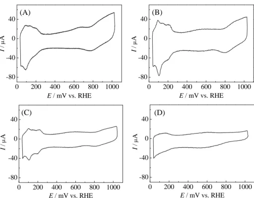
3.
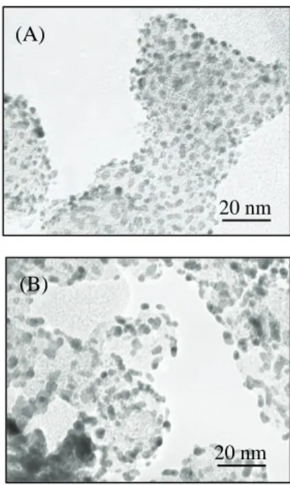
結果図
1(A)は調製試料(Pt
担持量: 24 wt.%)の典型的なTEM
像を示す。この試料では、黒点で表される
Pt
ナノ粒子が灰色のカーボン担体上に高分散に担持されている。この写真をXRF
の検量 線作成用に用いた市販試料(図1(B))と比べると、調製試料に担持された Pt
粒子は極めて均一で 凝集体も存在しないことがわかる。なお、調製試料に担持された
Pt
の平均粒径は市販試料の3.8 nm
より小さい2.1 nm
で あった。図
2
は電位掃引毎に測定したサイクリックボルタムグラ ムを示す。1回目に測定したボルタムグラムでは、水素の吸 脱着、およびPt
酸化物の形成と還元に起因する酸化・還元 電流[18]が、それぞれ41~300 mV vs. RHE
と650 mV vs. RHE
より貴な電位範囲に認められた(図2(A))。しかし、水素吸
脱着ピークはブロードであり、図2(A)のボルタムグラムは汚
れたPt
電極の結果に類似した[19]。一方、100回の連続掃引 後に測定したボルタムグラムは水素吸脱着ピークが明瞭に なり、清浄化されたPt
電極で得られる典型的なボルタムグ ラム[18]を示した(図2(B))。しかし、電位掃引回数が 500
回になると水素吸脱着電流は減少し(図2(C))、4000
回目 では水素吸脱着電流の減少がさらに顕著になった(図2(D))。
このようなサイクリックボルタムグラムの変化は新たに作 用電極を作製して連続電位掃引を行っても得られ、この測定 の再現性が高いことが明らかとなった。
20 nm (B)
20 nm (A)
Figure 1 Typical TEM images of
(A) prepared Pt/C sample (Pt: 24
wt.%) and (B) commercially
available Pt/C sample (Pt: 40
Pt
のボルタムグラムで観測される水素脱着アノード電流とESA
には以下の関係式が成り立つ[20]。
ESA (cm
2) = Q/210 (1)
ここで、Qは
Pt
上の水素脱着反応に起因する電荷 量(μC)、210はPt
単位面積辺りの水素脱着反応 から得られる電荷量(μC/cm2)を表す。この式を 用いて調製試料のボルタムグラムからESA
を求め、電位掃引回数に対してプロットした(n=2)。その 結果を図
3
に示す。電位掃引を100
回繰り返すとESA
は一旦増加する。これは、上記したPt
の清浄 化に起因すると考えられる。さらに電位掃引を繰 り返すとESA
は徐々に減少し、4000 回目のESA
は1
回目(0.74 cm2)の約20%に相当する 0.14 cm
2まで低下した。