Japan Advanced Institute of Science and Technology
JAIST Repository
https://dspace.jaist.ac.jp/
Title 小さなプローブ分子を用いた単層カーボンナノチュー
ブ電界効果トランジスタバイオセンサ
Author(s) Nguyen, Tung Thanh Citation
Issue Date 2019‑03
Type Thesis or Dissertation Text version ETD
URL http://hdl.handle.net/10119/15796 Rights
Description Supervisor:高村 禅, 先端科学技術研究科, 博士
NGUYEN THANH TUNG
Doctoral Dissertation
Single-walled carbon nanotube field-effect transistor biosensor using small probe
molecules
Supervisor: Prof. Yuzuru Takamura
Graduate School of Advanced Science and Technology Japan Advanced Institute of Science and Technology
Materials Science
March 2019
Abstract
Field-effect transistor (FET)-based biosensors offer many advantages such as real- time, label-free, fast response, portability, and high density integration in addition to its high sensitivity. However, generally FET-based biosensors face a critical issue of the Debye shield (physical length of approximately 1 nm induced by counterions in physiological environment) which limits the selection of probe molecules. Besides, conventional probe molecule such as antibody – a product of in vivo biological protocol, which is large in size (10 – 12 nm) and suffered from batch to batch activity variation, critical storage condition and high cost, is not suitable for FET-based biosensors.
In this study, we demonstrated the utilization of small in vitro probe molecules such as peptide aptamer and glutamate-binding protein (GBP) integrated with single- walled carbon nanotube (SWCNT)-FET to overcome aforementioned problems. The peptide aptamer and GBP are in vitro chemically synthesized. Therefore, their activities are uniform regardless of batch with extended storage time; synthesis is quicker and inexpensive; especially they can be flexibly modified to approach wide variety of target while antibody is limited. To implement this research, the following works have been done.
First, SWCNT-FETs were fabricated on the Si/SO2 substrate by growing SWCNTs on Co catalyst using catalytic alcohol chemical vapour deposition (CVD). We call this CVD-type SWCNT-FETs. On the other hand, to simplify the process of device fabrication and improve the reproducibility, a semiconducting SWCNT solution was used for the deposition of random network SWCNT. This technique is simple and fast, allowing a direct control of network density of SWCNT channel and hence the transistor characteristics. We call this network SWCNT-FET. Both CVD-type and network SWCNT-FETs exhibited typical p-type characteristics in ambient air and in solution as
well. The network SWCNT-FETs showed more reproducible operation than CVD-type SWCNT-FETs, but exhibited higher subthreshold swing value.
Second, we successfully integrated a novel peptide aptamer with the CVD-type SWCNT-FET to achieve highly sensitive and specific detection of biomarker. The novel peptide aptamer that specifically recognizes Cathepsin E (CatE) – a useful prognostic biomarker for cancer diagnosis, was utilized as probe molecule. The SWCNT channel was functionalized by no-covalent immobilization of the peptide aptamer using 1- pyrenebutanoic acid succinimidyl ester (PBASE) linker. As a result, the peptide aptamer- modified CVD-type SWCNT-FET could detect CatE at unprecedentedly low concentrations in both phosphate-buffered saline (0.1 ng/mL) and 10-times diluted human serum (10 ng/mL) and exhibited a high selectivity with no response to bovine serum albumin (BSA) and Cathepsin K (CatK)). The lowest detectable CatE of 10 ng/mL in serum is three time of magnitude lower than that of previous CatE biosensors. These results indicated that the use of small peptide aptamer is an effective strategy for realizing highly sensitive and selective FET-based biosensors. Our demonstrated sensor could be a promising platform for near-patient testing and point-of-care testing applications.
Third, we developed a new real-time monitoring Glutamate (Glu) sensor based on the integration of network SWCN-FET and glutamate-binding protein (GBP) for neuroscience application. Previous Glu sensors are suffered from the temporal and spatial resolution issues to monitor transient Glu. The bind and unbind event of Glu with its receptor is in millisecond range. Therefore, it is required to have a sensor system that is simple, miniaturizable and fast. The network SWCNT-FET appears as a promising candidate thanking to its properties of fast response, high reproducibility, real-time measurement and possibility to make a miniaturized device on flexible substrate.
Additionally, the GBP exhibits rapid recognition to transient Glu. Therefore, in this study,
we attempt to combine the GBP with the network SWCNT-FET for real-time monitoring transient Glu. To do that, the GBP probe molecule was immobilized onto the network SWCNT channel of network SWCNT-FET via PBASE linker. The resulting GBP- modified network SWCNT-FET sensor exhibited a high selectivity with no response to Dopamine (DA) and could detect Glu at micro-molar range in real-time. These results indicated that our sensor could be a promising candidate for Glu monitoring in real-time.
In conclusion, we have successfully demonstrated, for the first time, the integration of small probe molecules (peptide aptamer and GBP) into SWCNT-based FETs. The proposed platforms are promising for clinical application as well as neuroscience study, and be applicable for various target biomarkers.
Keywords: SWCNT-FET, peptide aptamer, Cathepsin E, Glutamate-binding protein, Glutamate.
Contents
Acknowledgements ... 6
Chapter 1: General introduction ... 7
1.1. Introduction to biosensors ... 7
1.2. Field effect transistor-based biosensors ... 11
1.3. Single-walled carbon nanotube field-effect transistor biosensors ... 12
1.4. Carbon nanotubes synthesis ... 16
1.5. Bio-immobilization methods on carbon nanotubes ... 21
1.6. Introduction to peptide aptamer ... 24
1.7. Introduction to Glutamate-binding protein ... 26
1.8. Goal of study ... 28
1.9. Overview of dissertation ... 28
Chapter 2: Investigation of single-walled carbon nanotube field-effect transistors ... 30
2.1. Introduction ... 30
2.2. Materials and apparatus ... 31
2.3. Experimental ... 33
2.3.1. Single-walled carbon nanotube synthesis using chemical vapour deposition.... 33
2.3.2. Fabrication of single-walled carbon nanotube field-effect transistor ... 35
2.3.3. Fabrication of network single-walled carbon nanotube field-effect transistor .. 36
2.3.4. Characterization of CVD-type SWCNT-FET and network SWCNT-FET ... 38
2.4. Results and discussion ... 40
2.4.1. Temperature and pressure dependence of SWCNT growth ... 40
2.4.2. Characterization of fabricated CVD-type SWCNT-FETs ... 43
2.4.3. Investigation of network SWCNT... 46
2.4.4. Characterization of fabricated network SWCNT-FETs ... 47
2.5. Conclusion ... 51
Chapter 3: Peptide aptamer-modified CVD-type SWCNT-FET biosensor ... 54
3.1. Introduction ... 54
3.2. Materials and apparatus ... 57
3.3. Experimental ... 58
3.3.1. Peptide aptamer characterization ... 58
3.3.2. Surface modification of the CVD-type SWCNT-FET and CatE detection scheme ... 59
3.3.3. AFM preparation of CatE captured on the peptide aptamer-modified CVD-type SWCNT-FET ... 61
3.3.4. Quantitative detection of CatE in 10-fold-diluted human serum ... 61
3.4. Results and discussion ... 61
3.4.1. Characterization of the peptide aptamer probe molecule ... 61
3.4.2. Quantitative detection of CatE in PBS buffer using the peptide aptamer- modified CVD-type SWCNT-FET biosensor ... 62
3.4.3. Quantitative detection of CatE in human serum ... 69
3.5. Conclusion ... 71
Chapter 4: Glutamate-binding protein modified network SWCNT-FET biosensor... 73
4.1. Introduction ... 73
4.2. Materials and apparatus ... 75
4.3. Experimental ... 76
4.3.1. Glutamate-binding protein characterization ... 76
4.3.2. Surface modification of network SWCNT-FET and Glutamate detection scheme ... 77
4.4. Results and discussion ... 80
4.4.1. Characterization of GBP probe molecule... 80
4.4.2. Glutamate detection using GBP-modified network SWCNT-FET sensor... 81
4.5. Conclusion ... 84
Chapter 5: Conclusion ... 86
5.1. Conclusion ... 86
References ... 87
Achievements ... 93
Appendix ... 96
6
Acknowledgements
First and foremost, I would like to thank my thesis supervisor, Prof. Yuzuru Takamura, who gave me the freedom and flexibility to be creative in research. It was my great honor to be a member of his research group. His kind advices and encouragement regarding this research are invaluable to me.
I would like to thank my committee members: Prof. Kenzo Maehashi from Institute of Engineering, Tokyo University of Agriculture and Technology; Prof. Hiroshi Mizuta, Assoc. Prof. Yuichi Hiratsuka and Assoc. Prof. Hidekazu Tsutsui from School of Materials Science, JAIST. I thank all of them for their time and consideration in serving on my dissertation committee.
My special thanks go to Assistant Prof. Phan Trong Tue for his enthusiastic supports and advices. I would like to express my thanks to Prof. Truong Thi Ngoc Lien at Hanoi University of Science and Technology, Vietnam; Prof. Biyani at JAIST, Prof. Ohno at Tokushima University, Prof. Maehashi at Tokyo University of Agriculture and Technology, Prof. Matsumoto at ISIR of Osaka University; who have kindly contributed to my research with the stimulating discussions. I would also like to thank Prof. Koyano who helped me take Raman spectra.
I would like to thank for the support of the Ministry of Education, Culture, Sports, Science and Technology (MEXT) during my study in Japan.
Many thanks go to my Lab members for fun activities we have shared as well as nice discussion. I would also like to thank all of the Vietnamese students at JAIST for the wonderful time we had.
Finally, and most importantly, I express my deepest gratitude to my family for their undying love and encouragement during my doctoral course.
JAIST, November 20th, 2019
Nguyen Thanh Tung
7 Chapter 1: General introduction
1.1. Introduction to biosensors
Biosensors are analytical devices that measure the presence of specific biological molecules by generating signals, which are proportional to the concentration of analytes in the samples. Biosensors offer applications on monitoring disease in the early stage, detecting pollutants in the environment or food safety aiming to improve the quality of life.
A typical biosensor consists of four components, namely probe molecule, linker, transducer and signal processing and displaying component (Figure 1.1).
Figure 1.1: Schematic structure of a common biosensor.
- A probe molecule (or bioreceptor) is a biological molecule that specifically recognizes the analyte in sample. The examples of probe molecules are antibody [1, 2], DNA probe [3, 4], and aptamer [5, 6] that is able to make the specific interaction with the target analyte such as antigen, complementary DNA, and target of aptamer. The interaction of the probe molecule with the analyte is term biorecognition, which determines the both specificity and sensitivity properties of a biosensor.
8
- A linker is a part of a biosensor that is used to immobilize the probe molecule onto the device. In other words, linker is an intermediate that joins the organically biochemical element to organic substrate. Choosing the suitable linker is important. The linker needs ensuring not only the mechanical immobilization but also the transfer of biorecognition signal to the transducer.
- A transducer is a part of biosensor that converts the signal from the binding of target analyte and probe molecule into a measurable signal. This generated signal is directly or inversely proportional to the amount of analyte-probe molecule interactions.
There are many types of transducer, namely electrochemical [7], optical [8], piezoelectric [9], thermal transducer [10], and micromechanical transducer (cantilever biosensor) [11, 12].
- A signal processing and displaying component is used to analyse the obtained signal then display on screen in a user-friendly way.
According to the principles of signal transduction (transducer) and birecognition element (probe molecule), biosensors can be classified as electrochemical biosensors (including potentiometric, amperometric and impedimetric biosnesors), calorimetric biosensors, optical biosensors, and acoustic biosensors (Table 1.1).
9
Table 1.1: The operation principle of biosensors.
Name Principle of operation
Potentiometric biosensor
- A type of electrochemical biosensor.
- The accumulation of a charge potential at working electrode is measured compared to the reference electrode when the current is equal or near zero.
Amperometric biosensor
- A type of electrochemical biosensor.
- The current that results from the oxidation or reduction of an electroactive species in a biochemical reaction, is measured while a constant potential is applied between working and reference electrodes.
Impedimetric biosensor
- A type of electrochemical biosensor.
- Based on monitoring the ability of an analyte to conduct an electrical current in a solution at constant voltage.
Calorimetric biosensor
- Based on measuring the change of temperature that is occurred in the reaction between biorecognition and analyte.
Optical biosensor
- Based on determining the change in light absorption between the reactants and products of a reaction or light emission.
Acoustic biosensor
- Based on piezoelectric phenomenon in which an oscillating crystal resonates at a natural resonance frequency.
Each type of biosensor has its own advantage and disadvantage as described in the Table 1.2.
10
Table 1.2: Advantage and disadvantage of biosensors.
Name Advantage Disadvantage
Potentiometric biosensor
- Simplicity of operation and the small size of the solid-state field effect transistor (FET) sensors.
- Less sensitivity (compared to amperometric biosensors) and nonspecific effects from other ion in the sample.
- Signal to noise ratio is analytical problem which is difficult to tackle.
Amperometric biosensor
- More sensitive, rapid, and inexpensive compared to
potentiometric and impedimetric biosensors.
- More suitable for mass production rather than potentiometric biosensor.
- The main disadvantage is having an indirect sensing system.
Impedimetric biosensor
- Applying for some promising approaches such as hybridization of DNA fragments amplified by a polymerase chain reaction [13].
- False positive results due to electrolytes from the samples.
- Less frequent than potentiometric and amperometric biosensors.
Calorimetric biosensor
- This method is capable in food industry and environmental monitoring [14].
- It is difficult to ensure that the temperature of the sample is constant.
Optical biosensor - Providing label-free real time detection.
- Can apply for single molecule detection [15].
- Expensive cost.
- It takes several hours and a technical training.
Acoustic biosensor
- Providing label-free and low cost biosensor.
- Requiring high stability of circuit and extremely high phase stability [16].
11 1.2. Field effect transistor-based biosensors
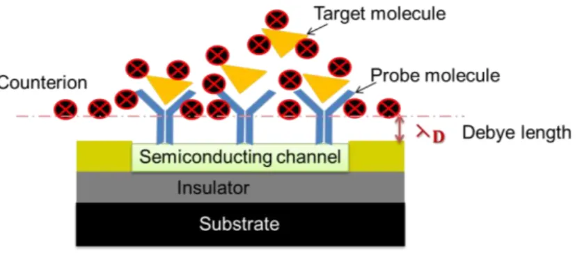
FET has been used as an attractive platform for the fabrication of integrated biosensors, which have drawn much attentions of scientist around the world owing to their outstanding benefits, such as a greater signal-to-noise ratio, fast measurement abilities, and portable instrumentation [17]. The FET-based biosensors offer many applications on detecting target analytes in gases [18-21], in solution [22, 23], and biomolecules in sample [24-26]. A FET consists of semiconducting channel and three electrodes (including source, drain and gate electrode). The detection mechanism of the FET-based biosensors is when the target analyte is in vicinity of the semiconducting channel, leading to the conductance of its channel changes accordingly. Therefore, the output electrical signal is changed proportionally to the amount of analyte concentration. Figure 1.2 depicts an example of an example of a FET biosensor. In which probe molecules are immobilized onto the semiconducting channel. The target molecules that are specifically attached to probe molecules will cause the static charge inside the semiconducting channel, leading to the change in conductance. There are many types of semiconducting materials to make the channel of FET-based biosensors such as carbon nanotubes [27], silicon nanowire [28] and graphene [29]. In which single-walled carbon nanotubes (SWCNTs) manifest many overwhelming properties, especially its one-dimensional structure. Therefore, in this work, we focused on SWCNT-FET-based biosensor.
Figure 1.2: Schematic structure of a field effect transistor (FET) biosensor.
12
The major drawback of all type of FET-based biosensor is short Debye length. It is argued that a FET-based biosensor can only detect the target analyte in very short distance away from its channel surface. This is because of the electrical double layer which screens off the charged biomolecules out of its. The Debye screening length is approximately 1 nm in physiological condition (Figure 1.3). So far, there are several ways to tackle this issue such as increasing Debye screening length by lowering salt concentration [30, 31]; using polyethylene glycol (PEG) [32]; or applying alternating current to weaken the electrical double layer [33]. However, all of these approaches have limitations. For example, using low ionic strength buffer solution would result in weakening the target-probe binding affinity. The use of AC makes system complicated and difficult to control. Etc. Recently, researchers have demonstrated small probe molecules as an effective way to overcome the Debye issue [5, 6].
Figure 1.3: Biomolecules carry the zero net charge because of Debye screening effect.
1.3. Single-walled carbon nanotube field-effect transistor biosensors
SWCNT was firstly synthesized by Sumio lijima and Toshinari Ichihashi in 1993 [34]. The first FET based on SWCNT was reported by Tans et al. [35] and Kong et al. used it to develop the first chemical sensor [36]. The functionalization of SWCNT based on principle of molecular recognition induces SWCNT-FET as one of the most promising candidates for the development of highly sensitive and label-free biosensors. SWCNTs
13
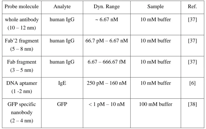
which are inherently small size compatible with biomolecules are straightforward to be modified with probe molecules, facilitating the great improvement of the selectivity and sensitivity of the current methods. Table 1.3 shows the comparison of CNT-FET biosensors that employed different probe molecules. Debye screening is the main issue for FET-based biosensor in general and for SWCNT-based FET biosensor in particular. The use of small probe molecule to bring the binding events close to the sensing surface of CNT-FET could enhance the impact of field-effect from charged biomolecule target, hence improving the sensitivity. As a result, the CNT-FET biosensor using Fab fragment (3 – 5 nm) could improve the minimal detectable concentration down to 1 pg/mL comparing to CNT-FET using whole antibody (10 – 12 nm) with detectable concentration of 1 µg/mL.
Additionally, the CNT-FET biosensors using DNA aptamer (1 -2 nm) and nanobody (2 -4 nm) probe molecules could detect IgE and GFP down to 250 pM and 1 pM, respectively.
In this work, we focused on using small probe molecules such as peptide aptamer (< 2 nm) and GBP (~ 5 nm) for SWCNT-based FET.
Table 1.3: Comparison of CNT-FET biosensors employed different probe molecules.
Probe molecule Analyte Dyn. Range Sample Ref.
whole antibody (10 – 12 nm)
human IgG ~ 6.67 nM 10 mM buffer [37]
Fab’2 fragment (5 – 8 nm)
human IgG 66.7 pM – 6.67 nM 10 mM buffer [37]
Fab fragment (3 – 5 nm)
human IgG 6.67 – 666.67 fM 10 mM buffer [37]
DNA aptamer (1 -2 nm)
IgE 250 pM – 160 nM 10 mM buffer [6]
GFP specific nanobody (2 – 4 nm)
GFP < 1 pM – 10 nM 100 mM buffer [38]
14
Figure 1.4 shows the schematic structure of a SWCNT-FET that consists of Si/SiO2
substrate, SWCNT channel and three electrodes (source, drain and gate electrodes). The carrier concentration inside SWCNT channel is manipulated by gate voltage. The negative or positive bias induces positive charges (holes) or negative charges (electrons), respectively [39]. SWCNT-FETs typically exhibit p-type characteristic under the ambient air because of the adsorption of oxygen molecules from air. The behaviour of SWCNT- FETs can change from p-type to n-type by passivation of SiNx with exposed groove of SWCNT channel [40]. Besides, the n-type SWCNT-FET can be fabricated by doping source and drain region with potassium [41].
Figure 1.4: Schematic structure of a SWCNT-FET.
Figure 1.5 shows the schematic structure of a SWCNT-FET biosensor. The bioreceptors are immobilized onto SWCNT sidewall via linker. The target biomolecules come and specifically bind to bioreceptor inside the sensitive region of Debye length.
Debye length is the distance around the SWCNTs that screen the surplus charge by the mobile carriers present in a material [42] (Figure 1.6). It depends on the salt concentration [C] with the formula √ ⁄ . In SWCNT-FET biosensors, the current through source and drain is measured. The origin of the current change is the field effect or a variation in the potential which is affected by the analyte concentration in the sample solution. Therefore, SWCNT-FETs are classified as potentiometric biosensors.
Drain SWCNT
SiO2
Si substrate Source
Gate
15
Figure 1.5: Schematic structure of s SWCNT-FET biosensor.
Figure 1.6: Schematic presentation of Debye length.
Consider a molecule in the vicinity of the CNTs, there are two main phenomena occurring. The first one is the charge transfer from the molecule to the CNTs channel. The second one is a scattering process in which the molecule acts as a scattering potential [43].
The charge transfer to the CNTs shifts the threshold voltage toward more positive or more negative direction in case of electron donation from the molecule to the CNTs or hole donation, respectively. If there is a scattering process, overall current decreases (Figure 1.7).
16
Figure 1.7: Current change in NTFET: (a) The effect of electron transfer from a protein to the CNTs; and (b) the reduction of carrier mobility by scattering potential created by a
protein.
1.4. Carbon nanotubes synthesis
CNTs are made of carbon atom by rolling up a graphene sheet with tubular nanostructure. There are two types of CNTs, single-walled carbon nanotube (SWCNTs) and multi-walled carbon nanotube (MWCNTs) (Figure 1.8). SWCNTs are generated from single sheet of graphite called graphene. MWCNTs are produced from either multiple sheets of graphite that are arranged in concentric cylinders (Russian Doll model) or single sheet of graphite that is rolled up into a tube (Parchment model). The interlayer distance in MWCNTs is approximately 0.34 nm. The diameters of SWCNTs and MWCNTs are approximately 0.8 to 2 nm and 5 to over 100 nm, respectively. The CNTs length is from several ten nanometers to several hundred nanometers [44]. SWCNTs can be either semiconducting or metallic depending on their chirality. One-third of as-grown SWCNTs are metallic while the rest are semiconducting [45, 46]. In contrast, MWCNTs usually exhibit a metallic property.
17
Figure 1.8: Schematic diagrams of SWCNT (left) and MWCNT (right) [47].
There are three main methods usually used to synthesize CNTs, namely arc discharge, laser ablation and chemical vapour deposition (CVD).
- Arc discharge is the method that was initially used by Iijima to discover CNTs in 1996 [48]. This technique generally consists of two high purity graphite electrodes called anode and cathode (Figure 1.9). The distance between anode and cathode is adjusted by moving the position of the anode. The inert gas is introduced at controlled pressure to make plasma between two electrodes. When the potential is applied between two electrodes, a discharge occurs, leading to formation of plasma. The products are obtained on the cathode. In case of no catalyst used, the products are the soot and deposit. The soot contains fullerenes while the carbon deposit contains MWCNTs together with graphite carbon nanoparticles. In case of a metal catalyst used along with graphite, most of nanotubes (SWCNTs and MWCNTs) are formed.
Figure 1.9: Schematic representation of arc discharge method.
18
- Laser ablation is the process in which an intense laser pulse is made to strike graphite target which contains small amount of metal catalyst such as nickel and cobalt, in a high temperature reactor with the presence of inert gas which vaporizes a graphite target (Figure 1.10). As a result, the inert gas is passed through the chamber carrying the synthesized nanotubes on the cooler surfaces of the reactor as the vaporized carbon condenses. This method chiefly produces SWCNT with higher purity than arc discharge process.
Figure 1.10: Schematic representation of laser ablation method.
Chemical vapour deposition (CVD) is the most popular method for high quality and large scale synthesis of carbon nanotubes. In this process, carbon feedstock gas (ethanol, ethylene, methanol or acetylene) is introduced into a high temperature (600 °C – 1200 °C) chamber that contains metal catalyst in either vacuum or atmospheric pressure (Figure 1.11). The catalytic metals are commonly Fe, Co and Ni because they make high solubility of carbon at high temperature and high carbon diffusion rate in these metals.
Additionally, Fe, Co and Ni have stronger adhesion with the growing CNTs than other transition metals; hence enable to form high curvature CNTs such as SWCNTs [49].
19
Figure 1.11: Schematic representation of chemical vapour deposition method.
Table 1.4 shows the comparison among three different methods for synthesizing CNTs. Compared to arc discharge and laser ablation methods, CVD method has many advantages. The energy required is lower. The carbon feedstocks are abundant and inexpensive. The setup of process is simple and it is easy to control and manipulate. In this process, CNTs are synthesized with high quality and large scale production [50]. The refining process is only necessary in case of further purification. Especially, CVD is unique method to produce well aligned CNTs which no other methods can make. With these aforementioned advantages, CVD method was chose to synthesize SWCNT in this work.
20
Table 1.4: Comparison of different synthesis methods of CNTs.
Method Arc discharge Laser ablation CVD
Typical yield 30 – 90 % Up to 70 % 20 – 100 %
SWCNT Short tubes with diameter of 0.6 – 1.4 nm
Long bundles of tubes (5 – 20 µm) with
individual diameter of 1 – 2 nm
Long tubes with diameter of 0.6 – 4 nm
Merits - SWCNTs with few defects
- MWCNTs without catalyst
- Relatively cheap - Open air synthesis possible
- Primarily SWCNTs with good diameter control and few defects - Quite pure
- Easiest to scale up - Simple process - Long length - SWCNT diameter is controllable - Quite pure
Demerits - Randomly short tube sizes and directions - Often needs purification
- Expensive because of costly lasers
- High power requirement
- Usually MWCNTs - Often riddled with defects
In CVD method, CNTs are formed via “tip-growth model” and “base-growth model” as shown in Figure 1.12. First, the carbon feedstock gas is decomposed, then deposited on the methal catalyst, thence CNTs is grown. In the “tip-growth model” (Figure 1.11(a)), the adhesion between substrate and metal particle is weak. When the hydrocarbon decomposes onto the top surface of metal particle, carbon diffuses into interface of metal particle and substrate, forming the CNTs and lifting up the metal particle until the metal particle is fully covered with excess carbon. In the “base-growth model” (Figure 1.11(b)),
21
the adhesion between substrate and metal particles is strong. When the hydrocarbon decomposes onto the surface of metal particle, carbon diffuses into the interface of metal particle and substrate. But in this case, it fails to push the metal particle. Therefore, it is compelled to emerge, hence forming CNTs.
Figure 1.12: Growth mechanism of CNTs: (a) tip-growth model, (b) base-growth model [49].
1.5. Bio-immobilization methods on carbon nanotubes
There are three types of adsorption methods: physical adsorption (physisorption), chemical adsorption (chemisorption) and entrapment method (Figure 1.13).
22
Figure 1.13: Three type of bioelement (probe molecule) immobilization.
Probe molecules can be immobilized onto sidewall of CNTs via covalent and nocovalent functionalization. In covalent method, probe molecules are immobilized directly onto defect of CNTs via covalent bond. In noncovalent method, probe molecules require a linker that mediates between them and CNTs.
Figure 1.14 shows the covalent functionalization of CNT’s sidewall. Firstly, carboxyl groups are formed on the defect of CNT’s sidewall by treating CNTs with strong acid like H2SO4 and HNO3 [51]. These carboxyl groups are treated with N- hydroxysuccinimide (NHS) and 1-Ethyl-3-(3-dimethylaminopropyl)carbodiimide (EDC) to make the semi-stable NHS ester. Then the biorecptors that contain the amide group are immobilized via amide bond and release NHS groups.
Figure 1.14: Covalent functionalization of CNT’s sidewall [52]
23
Figure 1.15 shows noncovalent pi-stacking functionalization of SWCNT. The 1- pyrenebutanoic acid succinimidyl ester (PBASE) is used as the linker to immobilized bioreceptor onto surface of SWCNT [5, 6, 53]. PBASE consist of aromatic rings in one tail and NHS group in another tail. The aromatic rings make π- π interaction with surface of SWCNT while NHS group makes amide bond with bioreceptor.
Figure 1.15: π- π stacking functionalization of SWCNT.
In addition, bimolecular receptors can be immobilized onto SWCNTs via polymeric layer functionalized with a molecular receptor, biotin that recognizes biomolecule, streptavidin [54] (Figure 1.16).
Figure 1.16: Modification of CNTs by polymeric layer containing biotin [54].
On the other hand, protein can directly bind to sensitive region of SWCNT-FET via electrostatic attraction. The substrate of SWCNT-FET is charged. Then protein with opposite charge comes and binds to the substrate [55] (Figure 1.17).
H2N
bioreceptor
O N O
O O C
O N O
O O C
SWCNT
1-Pyrenebutanoic acid succinimidyl ester
N O C
H
Amide bond
24
Figure 1.17: Schematic of poly-L-lysine (PLL) binding to SiO2 and a CNT [55].
1.6. Introduction to peptide aptamer
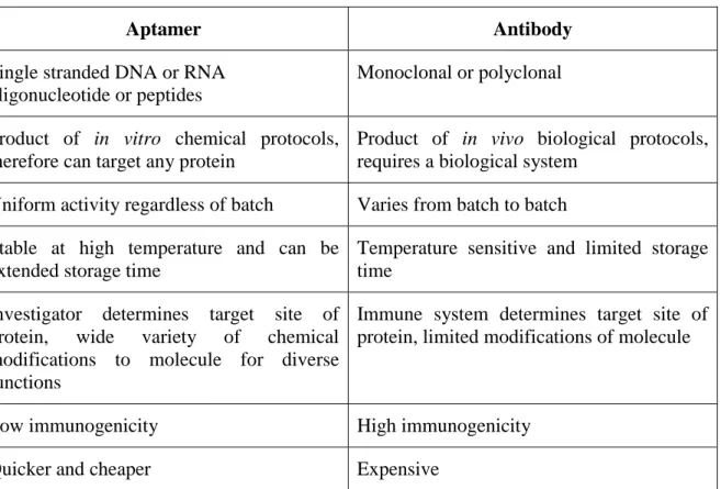
The aptamers have been discovered and developed as a substitutable probe molecule of antibody. Aptamer was known as a short single stranded folded oligonucleotides and peptide that bind to molecular targets with high affinity and specificity. Table 1.5 shows the comparison between aptamer and antibody.
Table 1.5: Comparison between aptamer and antibody.
Aptamer Antibody
Single stranded DNA or RNA oligonucleotide or peptides
Monoclonal or polyclonal Product of in vitro chemical protocols,
therefore can target any protein
Product of in vivo biological protocols, requires a biological system
Uniform activity regardless of batch Varies from batch to batch Stable at high temperature and can be
extended storage time
Temperature sensitive and limited storage time
Investigator determines target site of protein, wide variety of chemical modifications to molecule for diverse functions
Immune system determines target site of protein, limited modifications of molecule
Low immunogenicity High immunogenicity
Quicker and cheaper Expensive
25
Recently, peptide aptamers have been developed since 1996 by Pierre Colas et al.
[56]. Peptide aptamers are small artificial recognition proteins that consist a variable peptide sequence with affinity for a given target protein. This variable peptide sequence is inserted into the context of a small and very stable protein backbone, called “scaffold” [57- 62]. Peptide aptamers can be produced and selected in vivo from combinatorial libraries on the basis of their affinity to the target protein and expressed in bacterial cells such as E.
coli. Both termini of the variable peptide sequence are embedded (“double constrained”) within an inert and constant scaffold protein. This double constraint distinguishes peptide aptamer from other classes of constrained combinatorial proteins (such as antibodies, antibody fragments and other non-antibody scaffold-based molecules) which consist of random peptide sequences embedded to a carrier protein [63] (Figure 1.18). These recognition molecules are more complex than peptide aptamers because target-binding surfaces consist of non-contiguous peptidic sequences disseminated on several secondary structural elements or across several variable loops. Moreover, these molecules require disulfide bonds to fold properly and are thus ill suited to target intracellular proteins [57].
Figure 1.18: Comparison between different constrained combinatorial recognition proteins.
IgG, immunoglobulin G; scFv, single-chain Fv antibody fragment [59].
26
Peptide aptamers show the molecular recognition properties similar to antibodies, but with overwhelming characteristics including their small size, simple design, high stability, high solubility, high yield bacterial expression and their disulphide-independent folding. The comparison of peptide aptamer versus antibody and DNA aptamer is briefly shown in Table 1.6.
Table 1.6: Comparison of antibody, DNA aptamer and peptide aptamer (O and X indicate better and worse, respectively)
In comparison with DNA aptamers, peptide aptamers are relatively shorter in size with smaller binding footprint that allows more thorough and precise capture of target.
Therefore, with the same surface area, peptide aptamers provide higher binding-site density and lower background signal that arises from the nonspecific binding of target analyte [64]. Additionally, DNA aptamer is created from the combination of 4 types of nucleotides (Adenine (A), Thymine (T), Guanine (G) and Cytosine (C)) while peptide aptamer was synthesized from the combination of 20 amino acids. Therefore, peptide aptamer is potential for approaching wide and diversity targets of biomarker.
1.7. Introduction to Glutamate-binding protein
Glutamate-binding protein (GBP) is glutamate/aspartate import solute-binding protein that specifically recognizes Glu (Glu) – a main excitatory neurotransmitter in the central nervous system. GBP is a kind of amino acid-binding protein which consists of two globular domains linked by hinges, and its ligand-binding site is located in the cleft
27
between the two domains. GBP was firstly discovered and purified from E. coli K12 [65, 66]. The biochemical and genetic properties of GBP has been well characterized [65-69].
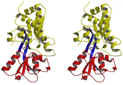
The crystal structure of a periplasmic glutamate/aspartate binding protein molecule has been determined as an ellipsoid size of approximately 55 × 45 × 40 Ả [70]. GBP binds to Glu through hydrogen bonds between side-chain and main-chain groups of GBP and the Glu as shown in Figure 1.19.
Figure 1.19: Structure of GBP. Domains I and II are colored yellow and red, respectively.
The two β-strands that connect domains I and II are colored blue. The bound glutamate molecule is shown as ball-and-stick model [70].
Comparisons with several other periplasmic amino acid binding proteins indicate that GBP residues involved in the binding of α-amino and α-carboxylate groups of the ligand (Glu) and the pattern of hydrogen bond formation between these groups are very well conserved, but the binding pocket around the ligand side chain is not, leading to the specificity of GBP [70].
Recently, Loren Looger’s lab developed the new GBP (iGluSnFr) by wedging green fluorescent protein (GFP) to periplasmic glutamate binding protein. When the resulting fusion protein binds to Glu, GBP’s conformational change leads to an increase in
28
fluorescence intensity from the inserted GFP [71, 72]. The result of characterizing iGluSnFr in vitro shows that it is selectively activated by Glu and exhibits rapid recognition to transient Glu in around 5 ms. This process of Glu transmission, which is in millisecond range, is related to the ability of learning and memory. Therefore, GBP plays a promising probe molecule to develop biosensor that can monitor Glu released from neurons and other brain cells in vivo for studying Glu signalling and regulation.
1.8. Goal of study
In this study, we aimed to demonstrate the integration of small probe molecules (such as peptide aptamer and GBP) into SWCNT-based FET. Firstly, we proposed the first demonstration of the integration of a novel peptide aptamer with the CVD-type SWCNT- FET to achieve highly sensitive and specific detection of biomarker in order to early diagnose cancer disease in clinical application. Secondly, we proposed the first demonstration of the integration of GBP and the network SWCNT-FET for real-time monitoring of transient Glu, which contributes on neuroscience study.
1.9. Overview of dissertation
Chapter 2 discusses the fabrication and characterization of CVD-type SWCNT- FET and network SWCNT-FET. The details of microfabrication such as photolithography and CNTs growth by CVD method are described. The operation and stability of the both fabricated CVD-type SWCNT-FET and network SWCNT-FET were investigated and evaluated for biosensing application.
Chapter 3 details the first demonstration of the successful integration of a novel peptide aptamer with a liquid-gated CVD-tyep SWCNT FET to achieve highly sensitive and specific detection of CatE, a useful prognostic biomarker for cancer diagnosis. Novel peptide aptamers that are engineered by systemic in vitro evolution to specifically
29
recognize CatE are small probe molecule. The SWCNTs were firstly grown using the thermal CVD method and then were employed as a channel to fabricate a CVD-type SWCNT-FET device. Next, the SWCNTs were functionalized by noncovalent immobilization of the peptide aptamer using PBASE linker. The resulting peptide aptamer- modified CVD-tyep SWCNT-FET sensors exhibited a high selectivity (no response to BSA and CatK) and label-free detection of CatE at unprecedentedly low concentrations in both phosphate-buffered saline (0.1 ng/mL) and human serum (10 ng/mL). Our results highlight the use of peptide aptamer-modified CVD-type SWCNT-FET sensors as a promising platform for near-patient testing and point-of-care testing applications.
Chapter 4 presents the first successful demonstration of the novel FET biosensor for Glu monitoring by integrating GBP probe molecule into network SWCNT-FET transducer. A PBASE linker is used to immobilize GBP probe molecule onto the network SWCNT channel of network SWCNT-FET device. The GBP-modified network SWCNT- FET could monitor Glu at micromolar range in real-time with high selectivity (no response to Dopamine). This scheme could be promising candidate for Glu signalling to study neuroscience.
30
Chapter 2: Investigation of single-walled carbon nanotube field-effect transistors 2.1. Introduction
With aforementioned reasons, we need high performance CVD-type SWCNT-FET for the integration with peptide aptamer to develop high-performance sensor. And we need network SWCNT-FET with high reproducibility and fast response for the integration with GBP to develop Glu-monitoring sensor. Therefore, in this chapter, we fabricated and characterized the CVD-type SWCNT-FET and network SWCNT-FET. The CNTs were synthesized using CVD method. Cobalt (Co) and ethanol were used as the catalyst and carbon source for CNTs growth. The pressure, temperature and growth time are key factors for growing CNTs. We investigated the conditions for SWCNT growth by varying the temperature from 650 to 850 °C, and pressure from 220 to 1200 Pa while keeping constant growth time of 30 min. The optimal condition of 300 Pa, 850 °C and 30 min was chosen for SWCNT growth. The photolithography micro-fabrication was used for the fabrication of source and drain electrodes to complete CVD-type SWCNT-FET. A solution-process and photolithography techniques were used for the fabrication of random network SWCNT-FET. This technique is easy and fast, allowing a direct control of network density of channel and thus the transistor characteristics. At first, the SiO2 surface of substrate was modified with (3-Aminopropyl)triethosysilane (APTES). A volume of commercial SWCNT was dropped on APTES-modified substrate and incubated to form the network SWCNT channel. The density of network SWCNT was investigated according to the incubation time of SWCNT solution from 20 min to 1h. The stabilities of operation of fabricated CVD-type SWCNT-FET and network SWCNT-FET were investigated.
31 2.2. Materials and apparatus
All chemicals and materials used in these experiments are listed in Table 2.1 below:
Table 2.1: List of chemicals and materials including their suppliers
Chemicals/materials and reagents Suppliers
Sulphuric acid H2SO4 Sigma-Aldrich
Hydrogen peroxide H2O2 Wako Pure Chemical Industries, Ltd.
OAP photoresist Tokyo Ohka Kogyo Co., Ltd., Japan
OFPR-800 photoresist Tokyo Ohka Kogyo Co., Ltd., Japan
LOR-10B photoresist MicroChem Corporation
Ethanol (super dehydrated, 95%) Wako Pure Chemical Industries, Ltd.
(3-Aminopropyl)triethosysilane (APTES) AVOCADO Research Chemicals Ltd., LANCS
SWCNT solution Meijo Nano Carbon Co., Ltd.
A 10× PBS stock solution was prepared by adding 80 g NaCl, 2 g KCl, 14.4 g Na2HPO4 and 2.4 g KH2PO4 into 1 L milli-Q water. The pH of PBS was adjust by adding NaOH or HCl.
32
All the apparatuses are listed in Table 2.2 below:
Table 2.2: List of apparatuses and their suppiers
Apparatus Suppliers
Sonicator AS ONE, Japan
Spin coater Mikasa, Japan
SiO2 100 nm/ p+-Si KST World Corp., Japan
pH meter Horiba, Japan
Mili Q system Barnstead Milli Q-purification system
Autopipette Eppendrof, Germany
Vortex IKA, Japan
E-beam evaporator MUE-ECO-EB ULVAC, Japan Scanning electron microscope (SEM)
model S-4500
Hitachi, Japan
Reference electrode Ag/AgCl Bioanalytical Systems, West LaFayette, IN
Agilent 4156C Precision Semiconductor Parameter Analyzer
Measure Jig Co., Ltd., Japan
The SEM and Raman spectroscopy methods were used to characterize the as- grown SWCNTs. The AFM method was used to visualize the capture of CatE by the peptide aptamer, which was immobilized onto the SWCNTs. The Agilent 4156C Precision Semiconductor Parameter Analyzer was utilized for measuring the electrical performance
33
of the pristine SWCNT FET and the electrical signals of peptide aptamer-modified SWCNT FET induced from binding events.
2.3. Experimental
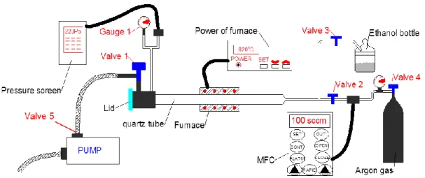
2.3.1. Single-walled carbon nanotube synthesis using chemical vapour deposition In this work, CVD method was used to synthesize SWCNT. The schematic structure of CVD system is shown in Figure 2.1. In this system, ethanol was used as the carbon source to synthesize SWCNT. Temperature was controlled by a temperature controller. Argon gas, which was managed by a mass-flow controller, was used to keep the pressure inside the chamber stably before and after supplying ethanol. A rotary pump was used to make vacuum inside the chamber. Chamber’s pressure value was displayed by a manometer.
Figure 2.1: Schematic structure of the CVD system for SWCNT synthesis.
Figure 2.2 shows the procedure of SWCNT synthesis by using CVD method.
Firstly, a commercial SiO2 (100nm)/p+-Si substrate was cleaned with piranha solution (a mixture of H2SO4 and H2O2 with ratio of 4:1 v/v). Then, two 5-nm-thick cobalt patterns were formed as the catalyst onto the substrate by using conventional photolithography and lift-off technology. The substrates were spin-coated with an OAP layer at 3000 rpm for 45
34
seconds followed by baking on a hot plate at 150 °C for 90 seconds. This OAP layer was used as a primer in order to improve adhesion between the substrate and photoresist. Next, OFPR-800 positive photoresist was spin-coated at 4000 rpm for 40 seconds, and then baked on a hot plate at 90 °C for 90 seconds. The samples were then exposed to UV light in a Double-View Mask Aligner PEM-800 for 3 seconds. The samples were developed in NMD3 for 60 seconds followed by rinsing with pure water. Next, cobalt thin film was deposited using an E-beam evaporator with deposition rate of 0.01 nm/s. The samples were then immersed in remover 106 for 15 minutes with sonication followed by rinsing with ethanol, 2-propanol and pure water to remove photoresist and residual organics. The substrate with Co catalyst patterns was introduced into the CVD system for SWCNT growth. Firstly, the quartz tube chamber was evacuated to around 10 Pa to pull out residual oxygen gas in the upper part of ethanol bottle at 800 °C. Then the furnace was cooled down in order to put the sample into chamber. The chamber was then evacuated while increasing temperature. After reaching a desired temperature, Ar gas (100 sccm) was introduced by mass flow controller for 10 minutes in order to get thermal equilibrium state of the whole system. Then ethanol was introduced into the chamber so that the pressure was kept fixed. After growing CNTs, the chamber was cooled down to room temperature naturally take out the sample.
35
Figure 2.2: The procedure of SWCNT synthesis.
In this work, two important parameters of the CVD process including growth temperature and pressure were investigated for optimizing SWCNT growth. In case of temperature dependence, CNTs growth was implemented at pressure of 1200 Pa for 30 minutes with variant temperatures. In case of pressure dependence, SWCNT growth was carried out at 850 °C for 30 minutes with variant pressures. The as-grown SWCNTs were confirmed by Raman spectroscopy. The morphology of as-grown SWCNTs was observed via SEM and AFM.
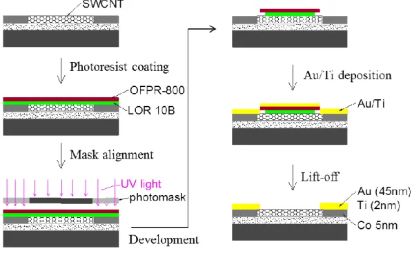
2.3.2. Fabrication of single-walled carbon nanotube field-effect transistor
After growing SWCNT, an array of Ti/Au (2 nm/45 nm) source and drain electrode pads were formed by using photolithography and lift-off technology (Figure 2.3). The distance between source and drain electrode was approximately 3 µm. The sample was
36
spin-coated with LOR 10B at 3000 rpm for 45 seconds, then baked on a hot plate at 150 °C for 3 minutes. This LOR 10B under layer was used to aid for the next metal lift-off process. OFPR-800 resist was then spin-coated at 4000 rpm for 40 seconds then baked on a hot plate at 90 °C for 90 seconds. Next, the samples were exposed to UV light in a contact aligner for 5 seconds. The samples were developed in NMD3 for 18 seconds followed by rinsing with pure water. Next, Ti (2 nm) and Au (45 nm) thin films were deposited by using e-beam evaporation with deposition rate of 0.01 nm/s and 0.03 nm/s, respectively. The samples were then immersed in remover 106 for 30 minutes at 70 °C in a hot plate followed by rinsing with ethanol, 2-propanol and pure water to remove photoresist and excess metal.
Figure 2.3: Deposition of Ti/Au electrodes to make CVD-type SWCNT-FET.
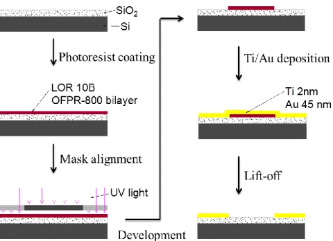
2.3.3. Fabrication of network single-walled carbon nanotube field-effect transistor We fabricated an array of network SWCNT-FETs onto a heavily doped p+-Si substrate capped with a 100 nm-thick thermally grown SiO2 layer. The p+-Si substrate was used as a back-gate electrode. First, a commercial SiO2(100nm)/p+-Si substrate was
37
cleaned with piranha solution (a mixture of H2SO4 and H2O2 with ratio of 4:1 v/v) at 100 °C for 10 min to modify SiO2 surface with hydroxyl group, followed by rinsing with milliQ water and drying with nitrogenous gas. An array of Ti/Au (2 nm/45 nm) source and drain electrode pads were formed by using photolithography and lift-off technique (Figure 2.4). The distance between source and drain electrodes was vary from 3 to 10 µm. The sample was spin-coated with LOR 10B at 3000 rpm for 45 seconds, then baked on a hot plate at 150 °C for 3 minutes. This LOR 10B under layer was used to aid for the next metal lift-off process. OFPR-800 resist was then spin-coated at 4000 rpm for 40 seconds then baked on a hot plate at 90 °C for 90 seconds. Next, the samples were exposed to UV light in a contact aligner for 5 seconds. The samples were developed in NMD3 for 18 seconds followed by rinsing with pure water. Next, Ti (2 nm) and Au (45 nm) thin films were deposited by using e-beam evaporation with deposition rate of 0.01 nm/s and 0.03 nm/s, respectively. The samples were then immersed in remover 106 for 30 minutes at 70 °C in a hot plate followed by rinsing with ethanol, 2-propanol and pure water to remove photoresist and excess metal.
Figure 2.4: Deposition of Ti/Au to make an array of source and drain electrode pads.
38
After making source and drain electrode pads, the network SWCNT was deposited onto the device as depicted in Figure 2.5. The SiO2 surface was modified with amine terminated groups of APTES self-assembled monolayer (SAM) by dropping a fresh solution of 5% APTES, 5% water and 90% pure ethanol for 2h at room temperature, followed by rinsing thoroughly with milli-Q water. Then the commercial SWCNT solution was dropped onto the APTES-modified substrate and incubated at room temperature for variant time (from 10 min to 1h) to form a network SWCNT, the specimen was rinsed with milli-Q water and dried with nitrogen gas. The device was baked at 200 °C for 30 min to remove the surfactant and to form good contacts between SWCNTs and electrodes.
Figure 2.5: Fabrication of network SWCNT-FET.
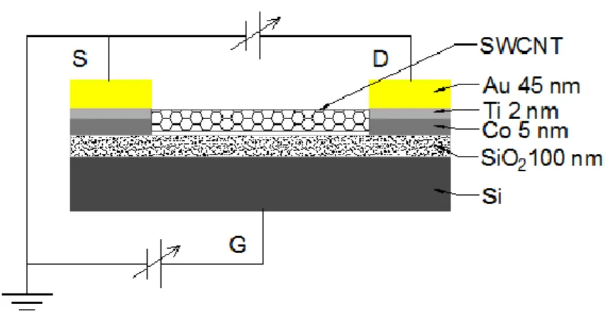
2.3.4. Characterization of CVD-type SWCNT-FET and network SWCNT-FET
In the FET, CVD-type SWCNTs and network SWCNTs function as a semiconducting channel. The both fabricated CVD-tyep SWCNT-FETs and network SWCNT-FETs were characterized with back-gated measurement setup by using Agilent 4156C Precision Semiconductor Parameter Analyzer as shown in Figure 2.6. The source electrode was grounded. In transfer characteristic (ID – VG) measurement, drain current was measured at a constant drain voltage and variant back-gated voltages. In output
39
characteristic (ID – VD) measurement, drain current was measured with a constant back- gated voltage and variant drain voltages.
Figure 2.6: Back-gated schematic circuit for measuring the electrical characteristics of both fabricated CVD-type SWCNT-FET and network SWCNT-FET.
The liquid-gated schematic circuit for measuring the electrical characteristics of fabricated CVD-type SWCNT-FETs and network SWCNT-FETs were carried out in order to compare the stable operation between back-gated and liquid-gated scheme (Figure 2.7).
The source electrode was grounded. The drain current was measured at a constant drain voltage of 200 mV and variant liquid-gated voltages from 0 to -0.6 V.
Figure 2.7: Liquid-gated schematic circuit for measuring the electrical characteristics of both fabricated CVD-type SWCNT-FET and network SWCNT-FET.
40 2.4. Results and discussion
2.4.1. Temperature and pressure dependence of SWCNT growth
The CNTs were grown between two cobalt patterns at a given pressure of 1200 Pa for 30 minutes. Figure 2.8 shows the SEM images of CNTs growth as a function of growth temperatures (650, 700, 750, 800, and 850 °C). The results indicated that SWCNTs started growing at 800 °C with increases in density and length.
Figure 2.8: SEM image of temperature dependence of SWCNT growth.
In order to confirm the as-grown SWCNTs, the Raman spectrum of SWCNTs was taken. Figure 2.9 shows the Raman spectrum of SWCNT grown at 1200 Pa of ethanol, 850°C for 30 minutes. These results clearly indicated that SWCNTs were successfully synthesized by CVD method. The characteristic radial breathing mode (RBM) of SWCNT was observed at 170 cm-1 corresponding to as-grown SWCNT’s diameter of around 1.4 nm [73].
41
Figure 2.9: Raman spectra of SWCNT that was synthesized at 1200 Pa of ethanol, 850°C for 30 minutes. Characteristic radial breathing mode (RBM) observed indicated SWCNT.
At lower temperatures (650°C, 700°C, 750°C), introduced ethanol might not be pyrolyzed properly, leading to the formation of multi-walled carbon nanotubes (MWCNTs). This result was confirmed by Raman spectrum as shown in Figure 2.10 with the G band at 1591 cm-1 assigned to the in-plane vibration of C-C bond and D band at 1342 cm-1 activated by the presence of disorder in carbon systems [74].
42
Figure 2.10: Raman spectra of single-walled nanohorn (SWNH) or damaged grapheme in case of CNTs synthesized at 1200 Pa of ethanol, 650°C for 30 minutes.
SWCNTs grown at 850°C appeared long enough to bridge between two cobalt patterns. Further, the SWCNT grown at 850°C also exhibited highest density compared to the other conditions. This fact could enable successful fabrication of CVD-type SWCNT- FET in which the grown SWCNT played a role as the transistor’s semiconducting channel.
Based on this investigation, 850°C was selected as the temperature for CNT growth.
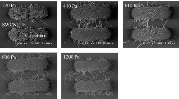
Figure 2.11 shows the SEM images of SWCNTs as a function of pressure (220, 410, 610, 800, and 1200 Pa) at 850°C for 30 min. SWCNTs were sparse at 220 Pa and denser at higher pressures (610 Pa, 800 Pa, and 1200 Pa). The flow rate of ethanol introduction is proportional with chamber pressure. At 220 Pa, a less amount of ethanol source was supplied, leading to sparse SWCNTs growth. At higher pressure, a larger amount of ethanol source was introduced, resulting in denser SWCNTs growth. These results indicated that SWCNTs could be able to synthesize in wide range of pressure (from 220 Pa to 1200 Pa) using CVD method.
43
Figure 2.11: SEM image of the pressure dependence of SWCNT growth.
2.4.2. Characterization of fabricated CVD-type SWCNT-FETs
Figure 2.12 shows the SEM image, taken at 1.0 keV acceleration voltage, of fabricated CVD-type SWCNT-FET focused on an area between source and drain electrodes. It is clearly seen that SWCNT was successfully bridged between these source and drain electrodes.
Figure 2.12: SEM image of fabricated CVD-type SWCNT-FET (white arrow indicates the SWCNT) and real photo of a fabricated chip, which contains an array of 52 SWCNT-FETs.
44
Figure 2.13 shows the transfer characteristics of 10 different CVD-type SWCNT- FETs devices. The back-gate in air was scanned from -5 to 5 V while drain voltage was kept constant of 0.5 V. The transfer curves vary from device to device. This variation may be due to the uncontrollable SWCNT growth during the CVD processes.
Figure 2.13: Transfer characteristics of 10 fabricated CVD-type SWCNT-FET devices Figure 2.14 shows the transfer characteristics of the fabricated CVD-type SWCNT- FET were measured using back-gated and top liquid-gated schemes. The back-gate bias in air was swept from -3.0 to 1.5 V. The liquid-gated bias was scanned from 0 to -0.6 V. Such a small liquid-gated voltage was used to prevent undesirable electrochemical reactions between the source/drain metal electrodes and the liquid [75]. In both measurements, the drain currents decreased with increasing gate voltage, indicating that hole conduction was dominant in the fabricated SWCNT FET. A similar tendency of the drain current versus gate voltage was also observed in the output characteristics (Figure 2.15). The top liquid- gated device exhibited a smaller subthreshold swing factor (S) (85.7 mV/decade) compared with that of the back-gated device (337 mV/decade). This small S-factor of the liquid-gated CVD-type SWCNT-FET was due to a large capacitance induced by the formation of an ultrathin electrical double layer in the vicinity of the SWCNT channel [76].
45
Generally, in the case of FET-based biosensors, a smaller S-factor indicates greater sensitivity.
Figure 2.14: Transfer characteristics of fabricated CVD-type SWCNT-FET using back- gated (black) and liquid-gated (red) measurement.
Figure 2.15: Output characteristics of fabricated CVD-type SWCNT-FET using (a) back- gated and (b) top-liquid-gated schemes. In both measurements, at source-drain voltage of
0.1 V, the drain currents decreased with increasing gate voltage.
Figure 2.16 shows the operation stability of CVD-type SWCNT-FET in air versus in liquid. The variation of transfer curves (∆V) at drain current of 80 nA are 345 mV and 29 mV, corresponding to back-gated and top liquid-gated scheme, respectively. The result indicated that the fabricated CVD-type SWCNT-FET manifested stable operation in
46
liquid-gated scheme rather than in ambient air scheme. This stability stems from the SWCNT channel being covered by the liquid, thereby preventing the effects of the surrounding environment. In addition, the use of an Ag/AgCl reference electrode can minimize voltage fluctuations [77]. These stability properties are critically important for realizing reliable biosensing devices.
Figure 2.16: Operation stability of CVD-type SWCNT-FET in air versus in liquid: The transfer characteristics of fabricated CVD-type SWCNT-FET with 10 measurements,
using (a) back-gated scheme and (b) top liquid-gated scheme.
2.4.3. Investigation of network SWCNT
The network SWCNT was evenly formed on the SiO2/Si substrate via APTES (Figure 2.17 (b)) in contrast to the substrate without APTES treatment (Figure 2.17 (a)).
The surface of substrate, which was modified with amine-terminated groups by APTES, is able to make the electrostatic attraction to the carboxyl groups of SWCNT. Therefore, the network SWCNT was deposited evenly on the APTES-modified Si/SiO2 substrate. On the other hand, the surface of substrate without APTES treatment, which was decorated by hydroxyl groups by treating with piranha solution, is not able to be deposited by SWCNTs.
47
Figure 2.17: SEM images of network SWCNT on Si/SO2 substrate (a) without and (b) with APTES treatment. SWCNT solution was incubated for 40 min.
Figure 2.18 shows incubation time dependence of network SWCNT density. The density of SWCNT is denser with longer incubation time. It is due to the accumulation of SWCNTs in the solution.
Figure 2.18: SEM images of network SWCNT on APTEST-modified Si/SiO2 substrate with variant incubation time of SWCNT solution from 20 min to 1h.
2.4.4. Characterization of fabricated network SWCNT-FETs
Figure 2.19 shows the SEM image of a network SWCNT-FET device with the semiconducting network SWCNT channel connecting two Au source and drain electrodes.
48
Figure 2.19: SEM image of a network SWCNT-FET with incubation time of SWCNT solution of 40 min.
The transfer characteristics of fabricated network SWCNT-FET with variant incubation time of SWCNT solution of 20, 40 and 60 min as shown in Figure 2.20. The back-gate in air was scanned from -10 to 10 V while drain voltage was kept constant of 0.2 V. The drain current decreases with increasing back-gated voltage. These results indicate that the fabricated network SWCNT-FET devices exhibit typical p-type characteristic. The both “on” and “off” currents of transfer curves increase with increasing incubation time of SWCNT solution from 20 to 60 min. This is due to the increase of carrier density inside network SWCNT channel which is originated from the denser network SWCNT formation at longer incubation time of SWCNT solution as aforementioned in Figure 2.18. The transfer curves of devices are unstable in case of sparse network SWCNT channel (Figure 2.20 (a)) and more stable in case of denser network SWCNT channel (Figure 2.20 (b, c)).
This may because of the inhomogeneous or impure SWCNT solution. It is difficult to completely remove the contamination or filter the semiconducting SWCNT from mixture of metallic and semiconducting SWCNT solution. With the devices fabricated in case of the incubation time of SWCNT solution of above 1h, the “on/off” ratio becomes smaller (data is not shown). It is due to the high amount of metallic SWCNT existing in the network SWCNT channel. Additionally, in case of long incubation time of SWCNT
49
solution, the SWCNTs were accumulated and created thick film of network SWCNT.
Therefore, higher back-gated voltage is required to deplete the hole carrier inside the network SWCNT channel. Based on these investigations, 40 min and 1 h are selected as the good condition for fabrication of network SWCNT-FET devices. Moreover, compared with the operation of the SWCNT-FET devices which were fabricated based on CVD method (as mentioned before in Figure 2.13), the operation of network SWCNT-FETs shows better stability from device to device. The stability of operation can be expected to be improved by using more homogeneous or pure SWCNT solution.
Figure 2.20: Transfer characteristics of network SWCNT-FETs with different incubation time of SWCNT solution: (a) 20 min, (b) 40 min and (c) 1h.
Figure 2.21 shows the transfer characteristics of the fabricated network SWCNT- FET were measured using back-gated and top liquid-gated schemes. The drain current was
50
kept constant at 0.2 V for both cases. The back-gate bias in air was swept from -5.0 to 1 V.
The liquid-gated bias was scanned from 0 to -0.6 V. Such a small liquid-gated voltage was used to prevent undesirable electrochemical reactions between the source/drain metal electrodes and the liquid. In both measurements, the drain currents decreased with increasing gate voltage, indicating that hole conduction was dominant in the fabricated network SWCNT FET. The top liquid-gated device exhibited a smaller subthreshold swing factor (S) (110 mV/decade) compared with that of the back-gated device (1.821 V/decade).
This small S-factor of the liquid-gated network SWCNT-FET was due to a large capacitance induced by the formation of an ultrathin electrical double layer in the vicinity of the SWCNT channel.
Figure 2.21: Transfer characteristics of fabricated network SWCNT-FET using back-gated (black) and liquid-gated (red) measurement.
Figure 2.22 shows the operation stability of fabricated network SWCNT-FET in air versus in liquid. The variation of transfer curves (∆V) at drain current of 100 nA are 147 mV and 12.7 mV, corresponding to back-gated and top liquid-gated scheme, respectively.
The result indicated that the fabricated SWCNT FET manifested stable operation in liquid- gated scheme rather than in ambient air scheme. This stability stems from the SWCNT
51
channel being covered by the liquid, thereby preventing the effects of the surrounding environment. In addition, the use of an Ag/AgCl reference electrode can minimize voltage fluctuations. These stability properties are critically important for realizing reliable
biosensing devices.
Figure 2.22: Operation stability of network SWCNT-FET in air versus in liquid: The transfer characteristics of fabricated network SWCNT-FET with 10 measurements, using
(a) back-gated scheme and (b) top liquid-gated scheme.
2.5. Conclusion
In this chapter, we first synthesized and optimized SWCNT growth by using the CVD method. Using the optimized SWCNT, we proceeded to the fabrication of CVD-type SWCNT-FET device. To simplify the process on fabricating device, a solution-process and photolithography technique were used for the fabrication of random network SWCNT- FET. The operation and stability of the both fabricated CVD-type SWCNT-FET and network SWCNT-FET were investigated and evaluated for biosensing application. The main achievements are summarized below:
- The CVD conditions such as growth temperature and pressure were systematically investigated for SWCNT growth. We found that the density, length and purity of grown