Power-Constrained Area and Time Co-Optimization for SoCs
Based on Consecutive Testability
Tomokazu Yoneda , Hisakazu Takakuwa and Hideo Fujiwara
Graduate School of Information Science, Nara Institute of Science and Technology
Keihanna Science City, 630-0192, Japan
yoneda, fujiwara @is.naist.jp
RICOH Japan.
Abstract
This paper presents a design-for-testability method that transforms a given SoC into consecutively testable one un- der power constraint. When a power constraint and a user defined importance ratio between area overhead and test time are given, the proposed method can create an optimal TAM design and a test schedule for the importance ratio under the power constraint with low computational cost. Experimental results show that the proposed method can achieve area and time co-optimization under power con- straint. Moreover, the proposed method can obtain better results for SoCs without power constraint compared to test bus method and our previous method based on consecutive testability of SoCs.
keywords: system-on-chip, test access mechanism, test scheduling, consecutive testability, power consumption
1 Introduction
In a core-based design environment, pre-designed, reusable megacells known as cores are integrated to de- sign an entire system on a single chip. This systems-on- chip (SoC) design strategies help companies to reduce the time-to-market and design cost for their new products sig- nificantly. However, testing of SoCs introduces several new challenges compared to testing of conventional IC designs [1]. The general problem of SoC test includes design of test access mechanism (TAM) architecture and test scheduling. The goal is to develop TAM and test schedule that mini- mize test time under given constraints. Recently, minimiza- tion of power consumption during test is becoming a major challenge for SoC designs.
A number of recent papers proposed several TAM ar- chitectures which include a dedicated test bus [2], TES- TRAIL [3] and transparency [4, 5] method. Moreover, vari- ous test scheduling methods are also proposed [6, 7, 8]. [6] presented a method for co-optimization of wrapper design and test scheduling based on an integer-linear programming (ILP) formulation. [7] proposed a 3D bin-packing formula- tion for test scheduling under power constraint.
In [12], we also proposed an ILP-based method for test time and TAM area co-optimization based on consecutive testability[9] and consecutive transparency [10]. In [9], we pointed out the necessity of consecutive test accessibility, which is the ability to apply an arbitrary test sequence to each core and observe its response sequence from the core consecutively at the speed of the system clock, in order to transport the given test sequence without information loss while the other methods based on transparency don’t have such accessibility. Since the consecutively transparent cores can provide paths for test data transportation of other cores, we can reduce area overhead of TAM by utilizing the cores’ consecutive transparencies . On the other hand, power con- sumption will increase since not only the core under test but also the other cores providing consecutively transparent paths consume power. Therefore, minimization of power consumption during test becomes more important when we use the consecutive transparency for the test access.
In this paper, we extend the previous method so that we can handle the power consumption problem. Moreover, we introduce efficient and effective heuristics to create a TAM and a test schedule based on the partitioned testing with run to completion(classified by Craig et al.[11]) while our previ- ous method are based on the non-partitioned testing and the ILP formulation. In the non-partitioned test scheduling ap- proach, test sets are grouped into sessions and new tests are allowed to start only when all test in the preceding session are completely executed. On the other hand, the approach based on partitioned testing with run to completion does not group tests into sessions, and new tests are therefore al- lowed to start at any time. Therefore, the proposed method can create an optimal TAM design and a test schedule for a given co-optimization ratio under power constraint with low computational cost. Experimental results show that the proposed method can achieve area and time co-optimization under power constraint. Moreover, the proposed method can obtain better results for SoCs without power constraint compared to test bus method and our previous method.
The rest of this paper is organized as follows. Section 2 gives SoC modeling and some definitions. In section 3, we show a power-conscious area and time co-optimization
IEEE the 14th Asian Test Symposium (ATS'05), pp. 150-155, Dec. 2005.
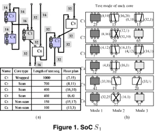
Figure 1. SoC
method that creates a TAM design and a test schedule. Ex- perimental results are discussed in section 4. Finally, sec- tion 5 concludes this paper.
2 Preliminaries 2.1 SoC Modeling
We assume that an SoC consists of cores, primary in- puts, primary outputs and interconnects and all cores oper- ate using single clock frequency. Moreover, an SoC has maximum allowable peak power consumption and floor plan denoted by coordinates of its center of grav- ity. For each core, a set of input/output ports, floor plan and a set of permissible configurations together with the peak power consumption are given. We consider three types of cores; IEEE 1500 wrapped cores (wrapped cores)[13], scan-designed cores (scan cores) and non-scan-designed cores (non-scan cores). Wrapped cores and scan cores have the input/output ports dedicated to test, and we consider that wrapped cores can be tested by using only the test ports. For each input/output port of a core, a set of test pattern sources (TPS)/test response sinks (TRS) required to test the core are given. The length of test/response sequence from the TPS/TRS are also given. Here, if TPS/TRS for a core is in- side(outside) of an SoC, it is said that the test method of the core is internal(external). We consider the following three types of configurations; test mode, CT (consecutively trans- parent) mode(see Section 2.2) and TPS/TRS mode. When a core is test mode, the core is under test. The CT mode core is providing paths for other test mode core. The TPS/TRS mode core is generating/observing test/response sequence for other test mode core. Figure 1 shows an example SoC we consider. Bit-width of each interconnect, the length of test/response sequence and the floor plan of each core are shown in Figure 1(a) and a set of configurations for each core are shown in Figure 1(b). Configuration 1 of each core represents test mode, and configuration 3 of core and represent TPS/TRS mode where the shaded ports are
generating/observing test/response sequence. Other config- urations represent CT mode where the shown paths are re- alizing.
2.2 Consecutive Transparency of a Core and Con- secutive Testability of an SoC
We introduced concepts called consecutive transparency of a core and consecutive testability of an SoC in [12].
Consecutive transparency of a core guarantees that, for each port of the core, there exists a test mode called a con- figuration which realizes consecutively transparent paths for the port. Here, paths are consecutively transparent in the sense that any test sequence can be propagated through them without information loss, and used for test/response sequence transportation for other core. In Figure 1(b), CT modes (mode 2 of all cores and mode 3 of core 1, 3 and 5) denote the configurations of the consecutively transparent cores where the paths with bit width and sequential depth shown in parentheses are realizing.
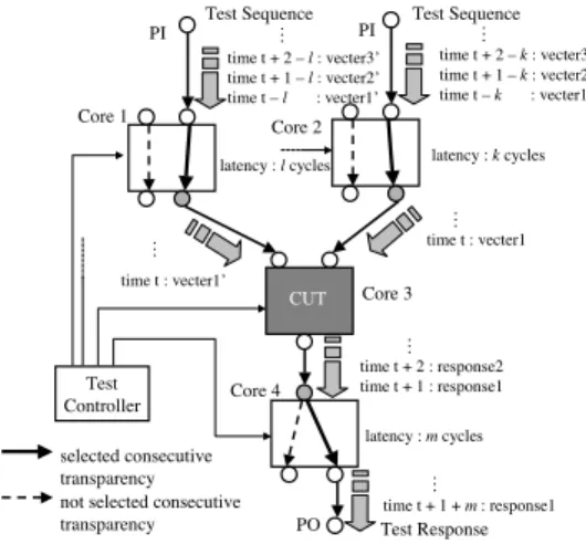
Consecutive testability of an SoC guarantees that it is possible to apply/observe arbitrary test/response sequences to/from all embedded cores and all interconnects with- out information loss by using interconnects and consecu- tively transparent cores. Figure 2 illustrates a consecutively testable SoC and the consecutive test access to/from Core 3. A control signal is provided for each consecutively trans- parent core by a test controller (either off-chip or on-chip) and determines the configuration of the core.
3 Power-Constrained Area and Time Co- Optimization
3.1 Problem Formulation
In this section, we present an area overhead and test time co-optimization method based on consecutive testabil- ity. When a power constraint and a user defined importance ratio between area overhead and test time are given, the pro- posed method creates TAM and a test schedule, and aug- ments a given SoC into consecutively testable one where area overhead and test time are co-optimized with respect to the ratio.
When we create consecutively test accessible TAM, we consider consecutive transparency, direct path (bus) from a PI to a core (from a core to a PO) with multiplexers and existing interconnect as the components of TAM. When a core is not consecutively test accessible by using only the existing interconnects and the consecutive transparency of cores, we make other cores consecutively transparent or we add direct paths to the core with multiplexers. Moreover, even if we can utilize a consecutively transparent core, we add a path to bypass the cores in order to reduce the power consumption during test.
The more DFT elements we add, the shorter test time we can achieve since it is possible to increase concurrency
CUT
Test Controller
PI PI
Test Sequence Test Sequence
time t + 2 – l : vecter3’ time t + 1 – l : vecter2’ time t – l : vecter1’
time t + 2 – k : vecter3 time t + 1 – k : vecter2 time t – k : vecter1
……
time t : vecter1’
… time t : vecter1
…
time t + 2 : response2 time t + 1 : response1
…
PO
time t + 1 + m : response1
…
Test Response Core 4
Core 3 Core 2 Core 1
latency : l cycles latency : k cycles
latency : m cycles selected consecutive
transparency not selected consecutive transparency
Figure 2. Consecutive test access
of test. There is a trade-off between area overhead and test time. Therefore, we formulate area overhead and test time co-optimization based on consecutive testability un- der power constraint as the following optimization problem. Definition 1 Power-constrained area and time co- optimization problem based on consecutive testability
Input : An SoC, co-optimization ratio
Output : A consecutively testable SoC (including TAM) and a test schedule
Constraint : peak power consumption and the number of SoC pins
Optimization : Minimizing the following equation (eq.(1))
(1)
3.2 Power-Constrained Area and Time Co- Optimization Algorithm
In this subsection, we describe the proposed algorithm (outlined in Figure 3, and detailed in Figure 4 and Figure 6).
(Step 1) We make all cores consecutively transparent using the method proposed in [10].
(Step 2) We compute the target test time and target test power which are the constraints in the schedul- ing step (Step 4) where the objective is to minimize the TAM area overhead. The main idea in this algorithm is to compute and that appropriately represent the user specified importance ratio between area overhead and test time. We compute for the given consid- ering the trade-off relation between test time and TAM area overhead as follows.
(2) (3)
Figure 3. Power-constrained area and time co- optimization algorithm
(4) Here, let be the test time of core , be the total bit-width of input/output pins of core .
The power consumption during test can be classified into the following three categories:power for the core in test mode , power for the core in CT mode and power for the core in TPS/TRS mode . When we al- low to consume more power for under , there exist many chances to achieve short test time since many cores can realize test mode simultaneously. On the other hand, when we allow to consume more power for , area overhead can be reduced since we can utilize many consec- utively transparent paths as TAM. Therefore, we compute for the given considering the trade-off relation among power, time and area as follows.
if is tested by external test
if is tested by internal test (5)
(6) Here, let be the power consumption of test mode
core and let be the summation of the
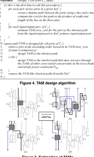
power consumption of TPS/TRS cores for core . (Step 3) We estimate the TAM (design temporary TAM) for each core assuming that the core is tested independently of other cores under no power constraint (detailed in Fig- ure 4). In this procedure, first, we create all the possible paths between ports that can be realized by a multiplexer and a bus, and calculate the cost of the path (from line 1 to 6). Then, we estimate the area cost for each port by finding the shortest path from the port to PI or PO (from line 6 to 9). After that, we design the temporary TAM for each port in the ascending order of the area cost by find-
Figure 4. TAM design algorithm
Figure 5. Estimation of TAMs
ing the independent shortest paths for the port (from line 10 to 18). From this temporary TAM design for each core, we can get the for the TAM and the set of cores that are used for testing the core. Examples of the esti- mated TAM for core , , and are shown in Fig- ure 5. Here, let be the set of cores that are used for testing . From Figure 5, we can see that ,
, ,
. Moreover, we compute the co-optimization cost for each core as follows.
(7) (Step 4) We create a test schedule (detailed in Figure 6). In the scheduling algorithm, we consider only and , and and are used as the test time and the test power constraints, respectively. The objective is to minimize the area overhead of the TAM design un- der the above constraints. For each core, we compute the TAM conflict ratio for each section (the minimal time in- terval separated by start or end time of some tests) as the measure to predict the area overhead of the designed TAMs (from line 1 to 3). We defined the TAM conflict ratio of core
Figure 6. Test scheduling algorithm
Figure 7. Conflict ratio of core for a section as follows.
(8) Here, let be the set of cores that is already scheduled in section , and let be the number of elements in . Examples of the TAM conflict ratio of core for all four sections are shown in Figure 7. Then, iteratively, we select a section in the ascending order based on its TAM conflict ratio, and find the best section that satisfies all constraints (from line 4 to 9). If there exists no section that satisfies all constraints for the core , we update as follows and do scheduling algorithm from the first core (from line 10 to 14).
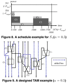
(9) Here, let be the core with the -th shortest test application time, and be the number of iteration of this process. Figure 8 shows the result of the test scheduling for the SoC in the case of .
(Step 5) We pick a core in the descending order based on its , and design the final TAM for in the similar fashion to Step 2 except for considering the created test schedule and power consumption for (from line 14 to 16 in Figure 4). In this step, we design the TAM under the power constraint . We can consume at least
power for the CT mode cores in order to reduce the TAM area overhead since we constrained the power for
and to during the test scheduling
step. Figure 9 shows the result of the added paths as the TAM of the SoC in the case of .
Figure 8. A schedule example for ( )
Figure 9. A designed TAM example ( )
4 Experimental Results
In this section, we present the experimental results ob- tained on a SunBlade 1000 workstation (900 MHz with 1GB RAM). Since our approach cannot apply the SoCs that have no information about connectivity between cores, it is not possible to make experiments by using ITC’02 SoC benchmarks. Therefore, in this section, we present the ex- perimental results for 3 randomly created SoCs. Charac- teristic and connectivity information of SoC are shown in Figure 1. Characteristics and connectivity informations of other two SoCs are shown in Table 1 and Figure 10, re- spectively. In Table 1, first four columns denote the name of SoC, the number of SoC input/output pins , floor plan represented by coordinates of its center of gravity, and the number of cores, respectively. “in.” and “ex.” at the column “TPS/TRS” denote the number of cores which can be tested by internal and external test, respectively.
“wrapped”, “scan” and “non-scan” at the column “DFT” denote the number of cores classified by their DFT tech- nique. For each core, we gave a test time and a peak power consumption randomly within the range shown in column
“time” and “power”, respectively. In this experiments, we assume that each core has the same power consumption for all configurations.
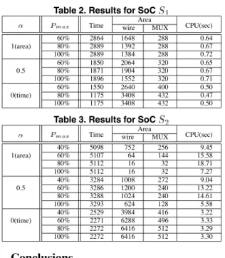
Table 2, 3 and 4 show the results for , and , re- spectively. In the tables, column “ ” denotes the max- imum allowable peak power of the SoC that is the percent- age for the summation of the peak power consumption of all cores. “Time”, “Area” and “CPU” denote test time, area overhead and computational time, respectively. “wire” at the column “Area” denote the wire area estimated as the product of width and length on the floor plan. We use the
Figure 10. Connectivity information for SoC
Table 1. Characteristics of three target SoCs
SoC(#PI,#PO)pin floorplan #coreTPS/TRSin. ex. wrapped scan non-scanDFT time power (160,96) (20,20) 6 3 3 1 2 3 0-1000 0-100 (64,64) (50,50) 11 1 10 3 2 6 0-1000 0-1000 (160,96) (100,100) 22 1 21 3 3 16 0-10000 0-5000
Manhattan distance for calculating length of wires. “MUX” at the column “Area” denote the total number of bit width of the added multiplexers. From all these tables, we observe that the proposed method can allow trade-off between area overhead and test time according to user defined ration under the given power constraint.
Table 5 shows the results for without considering power constraint. In this table, we make a comparison between the proposed method and other two methods in order to show the effectiveness of the proposed method.
“Testbus[9]” denotes the method based on test bus archi- tecture in [9]. “CT ILP[9]” denotes the method based on consecutive testability in [9]. From this table, we ob- serve that the proposed method can also achieve area and time co-optimization for a given co-optimization ratio un- der no power constraint. Moreover, the proposed method can achieve lowest area overhead for all three . Espe- cially, when , the proposed method can achieve 70% and 50% reduction of area overhead for “Testbus” and
“CT ILP”, respectively. This is because we considered all the possible paths between two ports as the DFT candi- dates in Design TAM procedure while only the paths be- tween PI(PO) and core’s input(output) port were taken into account in the previous methods. When , the pro- posed method can also achieve 50% reduction of test time for “CT ILP”, and the same test time for “Testbus”. This is because “Testbus” and the proposed method are based on partitioned testing with run to completion while “CT ILP” is based on non-partitioned testing. Computational time of the proposed method is negligible for all cases compared to the other two methods. Therefore, we conclude that the proposed method can create a TAM and a test schedule ef- ficiently and effectively compared to our previous methods.
Table 2. Results for SoC
Time wireAreaMUX CPU(sec)
60% 2864 1648 288 0.64
1(area) 80% 2889 1392 288 0.67
100% 2889 1384 288 0.72
60% 1850 2064 320 0.65
0.5 80% 1871 1904 320 0.67
100% 1896 1552 320 0.71
60% 1550 2640 400 0.50
0(time) 80% 1175 3408 432 0.47
100% 1175 3408 432 0.50
Table 3. Results for SoC
Time wireAreaMUX CPU(sec)
40% 5098 752 256 9.45
1(area) 60% 5107 64 144 15.58
80% 5112 16 32 18.71
100% 5112 16 32 7.27
40% 3284 1008 272 9.04
0.5 60% 3286 1200 240 13.22
80% 3288 1024 240 14.61
100% 3293 624 128 5.58
40% 2529 3984 416 3.22
0(time) 60% 2271 6288 496 3.33
80% 2272 6416 512 3.29
100% 2272 6416 512 3.30
5 Conclusions
This paper proposed a design-for-testability method that transforms a given SoC into consecutively testable one un- der power constraint. In the proposed method, we intro- duced efficient and effective heuristics to reduce the com- putational cost compared to our previous method base on ILP formulation. Therefore, the proposed method can cre- ate an optimal TAM and a test schedule for a given co- optimization ratio with low computational cost. Experimen- tal results show that the proposed method can achieve area and time co-optimization under power constraint. More- over, the proposed method can obtain better results for the SoCs without power constraint compared to test bus method and our previous method based on consecutive testability of SoCs. Especially for the case that area has high priority, the proposed method can achieve 70% and 50% reduction of area overhead compared to test bus approach and our previ- ous method based on consecutive testability, respectively. Acknowledgments
This work was supported in part by Japan Society for the Promotion of Science (JSPS) under Grants-in-Aid for Sci- entific Research B(2)(No. 15300018). The authors would like to thank Prof. Michiko Inoue, Prof. Satoshi Ohtake (Nara Institute of Science and Technology) for their valu- able discussion.
References
[1] Y. Zorian, E.J. Marinissen and S. Dey,“Testing embedded-core based system chips,” Proc. 1998 Int. Test Conf., pp.130–143, Oct. 1998. [2] S. Bhatia, T. Gheewala and P. Varma, “A unifying methodology for
intellectual property and custom logic testing,” Proc. 1996 Int. Test Conf., pp.639–648, Oct. 1996.
Table 4. Results for SoC
Time wireArea MUX CPU(sec)
20% 93614 13632 1696 132.06
40% 94736 7264 1600 375.41
1(area) 60% 94752 3840 1440 477.95
80% 94764 3072 1376 453.90
100% 94774 2560 1184 460.60
20% 64237 19104 1696 77.89
40% 64238 16448 1664 198.99
0.5 60% 64254 9728 1696 493.66
80% 64255 8384 1696 486.74
100% 64260 7392 1504 496.33
20% 39736 52224 2080 65.87
40% 34513 104928 2944 33.84
0(time) 60% 34516 115232 3232 32.79
80% 34516 120736 3360 32.67
100% 34516 125024 3392 32.65
Table 5. Results for SoC without power con- straint
method Time wireAreaMUX CPU(m)
TestBus[9] 1650 2774 528 0
1 CT ILP[9] 2125 1432 260 40
(area) proposed 2916 864 320 0
TestBus[9] 1250 2984 528 20
0.5 CT ILP[9] 1830 2144 316 0.2
proposed 1950 872 320 0
TestBus[9] 1000 3248 516 243
0 CT ILP[9] 1500 2736 396 22
(time) proposed 1000 2272 448 0
[3] E. Marinissen, R. Arendsen, G. Bos, H. Dingemanse, M. Lousberg and C. Wouters, “A structured and scalable mechanism for test access to embedded reusable cores,” Proc. 1998 Int. Test Conf., pp.284–293, Oct. 1998.
[4] M. Nourani and C.A. Papachristou, “Structural fault testing of em- bedded cores using pipelining,” Journal of Electronic Testing:Theory and Applications 15(1-2), pp.129–144, Aug.–Oct. 1999.
[5] S. Ravi, G. Lakshminarayana, and N.K. Jha, “ Testing of core-based systems-on-a-chip,” IEEE Trans. on CAD, vol.20, no.3, pp.426–439, Mar. 2001.
[6] V. Iyengar and K. Chakrabarty, “Test Wrapper and Test Access Mechanism Co-Optimization for System-on-Chip,” Journal of Elec- tronic Testing: Theory and Applications, vol.18, pp.213–230, Apr. 2002.
[7] Y. Huang, N. Mukherjee, S. Reddy, C. Tsai, W. Cheng, O. Samman, P. Reuter and Y. Zaidan, “Optimal core wrapper width selection and SOC test scheduling based on 3-dimensional bin packing algorithm,” Proc. 2002 Int. Test Conf., pp.74–82, Oct. 2002.
[8] E. Larsson and Z. Peng, “A reconfigurable power-conscious core wrapper and its application to SOC test scheduling,” Proc. 2003 Int. Test Conf., pp.1135–1144, Sep. 2003.
[9] T. Yoneda, T. Uchiyama and H. Fujiwara, “Area and time co- optimization for system-on-a-chip based on consecutive testability,” Proc. 2003 Int. Test Conf., pp.415–422, Sep. 2003.
[10] T. Yoneda and H. Fujiwara, “Design for consecutive transparency of cores in system-on-a-chip,” Proc. 21th VLSI Test Symp., pp.287– 292, Apr. 2003.
[11] G. L. Craig, C. R. Kime, and K. K. Saluja, “Test scheduling and control for VLSI built-in-self-test,” IEEE Trans. Comput., vol. 37, pp.1099–1109, Sept. 1988.
[12] T. Yoneda and H. Fujiwara, “Design for consecutive testability of systems-on-a-chip based on built-in self testable cores,” Journal of Electronic Testing: Theory and Applications, pp.487–501, Aug. 2002.
[13] E.J. Marinissen, R. Kapur, M. Lousberg, T. McLaurin, M. Ric- chetti and Y. Zorian, “On IEEE P1500’s Standard for Embedded Core Test,” Journal of Electronic Testing: Theory and Applications, pp.365–383, Aug. 2002.