A Non-scan DFT Method at RTL Based on Fixed-control Testability
to Achieve 100% Fault Efficiency
Satoshi Ohtake Shintaro Nagai Hiroki Wada Hideo Fujiwara
Graduate School of Information Science, Nara Institute of Science and Technology 8916-5, Takayama, Ikoma, Nara 630-0101, Japan
E-mail: ohtake, shinta-n, hiroki-w, fujiwara @is.aist-nara.ac.jp
Abstract This paper proposes a non-scan design-for-test- ability method for register-transfer level circuits where a cir- cuit consists of a controller and a data path. It achieves com- plete fault efficiency with low hardware overhead and at-speed testing.
1. Introduction
With the advance in semiconductor technology, the com- plexity of VLSI designs is growing and the cost of testing is increasing. Therefore, it is necessary to reduce the cost of test- ing and to enhance the quality of testing. The cost of testing is estimated by test generation time and test application time. The quality of testing is estimated by fault efficiency1. Therefore, we have to reduce test generation time and test application time and to enhance fault efficiency. To ease the complexity of test generation, design-for-testability (DFT) techniques have been proposed. The most commonly used DFT techniques for se- quential circuits are scan-based approaches[1]. These tech- niques modify sequential circuits so that automatic test pattern generation (ATPG) tools can achieve high fault efficiency in a reasonable time. However, these techniques sacrifice the pos- sibility of at-speed testing[2] for fault efficiency enhancement. To avoid this disadvantage of scan techniques, several non- scan approaches have been investigated. On the other hand, since techniques of test generation and DFT at gate level face the problems arising out of huge number of elements and high complexities of the circuits at gate level, several techniques of test generation and DFT at register-transfer level (RTL) have been proposed recently.
In RTL design, a VLSI circuit is generally consists of two separate parts, a controller part and a data path part. The for- mer is represented by a state transition graph (STG) and the latter is represented by hardware elements (e.g. registers, mul- tiplexers and operational modules) and signal lines connecting them. A controller and a data path are interconnected by in- ternal signals: control signals and status signals. Most of the DFT methods for RTL circuits were concerned with only ei- ther data paths or controllers, on the assumption that the con- trol signals and the status signals are directly controllable and observable from the outside of the VLSI.
For controllers, Chakradhar et al.[3] proposed a non-scan DFT method at RTL. This method can achieve high fault ef- ficiency but cannot always guarantee complete (100%) fault efficiency. Furthermore, it is applicable only to PLA-based se- quential circuits. Our previous work [4, 5] proposed several non-scan DFT methods which achieve 100% fault efficiency. In these methods, given an STG, we first synthesize a sequen- tial circuit from the STG. Then we generate test patterns, by
1Fault efficiency is the ratio of the number of faults detected and proved redundant to the total number of faults.
a combinational ATPG tool, for the combinational part of the synthesized sequential circuit. Most of the generated test pat- terns can be applied to the combinational part of the sequential circuit using state transitions of the STG. However, there may exist some test patterns which cannot be applied using state transitions of the STG. In this case, we append an extra logic which provides extra transitions required for testing. Those test patterns are applied using the extra logic.
For data paths, several non-scan DFT methods at RTL have been reported, e.g. orthogonal scan[6, 7] and H-SCAN[8], which use normal data path flow as scan path instead of tra- ditional scan path flow. These methods can reduce hardware overhead and test application time compared to the full-scan design. However, test generation time cannot be reduced be- cause the test generation approach is the same as the full-scan design. To reduce test generation time, a hierarchical test gen- erationapproach was proposed by Murray and Hayes[9]. The hierarchical test generation of a data path consists of the fol- lowing two steps: for individual combinational hardware el- ements, generate test patterns at gate level and generate test plansat RTL, where a test plan is a control sequence to prop- agate test patterns for a combinational hardware element from the primary inputs to the inputs of the hardware element and to propagate responses from the output of the hardware ele- ment to the primary outputs. Genesis [10]–[13] is an approach based on such a hierarchical test generation for data paths. Our previous work [14] presented a DFT method based on such hi- erarchical test generation and strong testability. Strong testa- bility is a property of data paths which guarantees to generate test plans for all combinational hardware elements of the data path.
In our previous work [15], we proposed a DFT method for an RTL circuit which consists of a controller part and a data path part. Given an RTL controller/data path circuit, we apply the DFT method of [4] to the controller part and apply that of [14] to the data path part. Our previous experimental results using benchmark circuits show that the hardware overheads of [4] and [14] were 3.5% and 4.0% on average for benchmark circuits, respectively. The test application times in [4] and [14] were reduced on average to 25.4% and 17.6% of the full-scan design, respectively. Furthermore, both of these DFT methods can achieve 100% fault efficiency and allow at-speed testing.
In the above-mentioned DFT methods, we assumed that both control signals and status signals between a controller and a data path are directly controllable and observable from the outside of circuits. However, if we consider a DFT method for the whole circuit consisting of both a controller and a data path, we have to remove this assumption by adding some extra logic to provide both controllability and observability of those con- trol and status signals. In our previous work [15], we resolved this problem by (1) adding multiplexers on those control and
IEEE 2000 Int. Workshop on RTL ATPG & DFT (WRTLT2000), pp. 61-77, Sept. 2000.
Controller Data Path
Control Signals (CSs)
Status Signals (SSs)
Primary Inputs(PIs)
Primary Outputs(POs) Primary Inputs(PIs)
Primary Outputs(POs)
COs CIs
SIs SOs
CIs: Control Inputs SOs: Status Outputs COs: Control Outputs
SIs: Status Inputs
Figure 1: An RTL controller/data path circuit.
status signals to connect directly from primary inputs and to primary outputs and (2) embedding an extra circuit in the con- troller side, called a test plan generator, which can generate test plans for the data path of an RTL circuit.
The proposed DFT method for controller/data path circuits has the following advantages:
100% fault efficiency can be achieved. At-speed testing can be performed. Furthermore, from our experimental results,
Test application time can be reduced significantly com- pared to the full-scan design.
Test generation time can be reduced significantly com- pared to the full-scan design.
However, the proposed method has the following disadvan- tage:
The hardware overhead is larger than that of the full-scan design.
The hardware overhead of the proposed method is domi- nated by extra logic corresponding to test plan generators for strongly testable data paths.
In this paper, we present a new property of circuit structure of data paths called fixed-control testability. If a data path is fixed-control testable, hierarchical test generation can be ap- plied and each test plan of combinational hardware elements can be composed of at most three control vectors. Therefore, a design of a test plan generator which generates test plans of the fixed-control testable data path is simpler than that of strongly testable one.
In this paper, we also propose a DFT method for data paths which makes a data path fixed-control testable and a test ar- chitecture for a whole circuit consisting of both a controller modified by [4] and a data path modified by the DFT method based on fixed-control testability proposed in this paper.
This paper is organized as follows: Section 2 gives the def- inition of controller/data path circuits and Section 3 shows overview of our DFT method. In Section 4, we introduce the DFT method of controllers reported in [4]. Section 5 presents a DFT method of data paths based on fixed-control testability. Section 6 presents a DFT method for whole circuits consisting of both controllers and data paths. Section 7 shows experi- mental results of the proposed method using some benchmark circuits and shows that our method proposed in this paper can reduce hardware overhead compared with that in [15].
2. Preliminaries
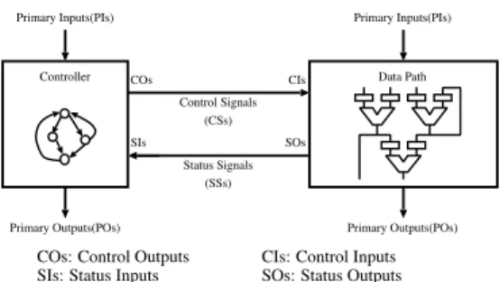
In RTL description, a VLSI circuit generally consists of a controller and a data path as shown in Figure 1. The for-
mer is represented by an STG and the latter is represented by hardware elements (e.g. registers, multiplexers and operational modules) and signal lines connecting them. Each of the con- troller and the data path has primary inputs from the outside of the VLSI and primary outputs to the outside of the VLSI. The controller also has status inputs from the data path and control outputsto the data path. Similarly, the data path also has control inputs from the controller and status outputs to the controller. The signals from the controller to the data path are called control signals, and the signals from the data path to the controller are called status signals.
Data path
A data path consists of hardware elements and signal lines. Hardware elements are primary inputs, primary outputs, con- trol inputs, status outputs, registers, multiplexors, and opera- tional modules. A signal line connects two hardware elements with some bit width. Inputs of a hardware element in the data path can be classified into data inputs and control inputs. Ex- amples of the control inputs are load enable signals of registers, selection signals of multiplexers and function selection signals of operational modules. Similarly, outputs of a hardware ele- ment of a data path can be classified into data outputs and sta- tus outputs. Comparators are examples of hardware elements having status outputs.
The following restrictions are introduced into our data path architecture in order to simplify the discussion, though they can be relaxed.
A1: All signal lines in the data path have the same bit width. A2: An operational module has only one or two data inputs
and only one data output.
A3: For any data input, there exists a path from a primary in- put. And for any data output, there exists a path to a pri- mary output.
A4: Control inputs of a hardware element are connected di- rectly to control inputs of the data path. And status out- puts of a hardware element are connected directly to sta- tus outputs of the data path.
3. Overview
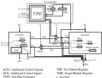
In our DFT method, given a controller/data path circuit de- scribed at RTL, we first apply the DFT method of [4] to the controller and apply the DFT method proposed in Section 5 to the data path of the circuit. In these DFT methods, we assume that the control signals and the status signals are directly con- trollable and observable from the outside of the circuit. How- ever, these are internal signals between the controller and the data path in the controller/data path circuit. Thus, for testing of the controller, we have to enhance controllability of the status inputs and observability of the control outputs. Similarly, for testing of the data path, we have to enhance controllability of the control inputs and observability of the status outputs. In the DFT method proposed in this paper, we embed mechanisms to enhance controllability and observability of the control signals and the status signals in the same way as the method of [15] so that the testing methods of controllers and data paths can be applied. The test architecture of the controller/data path circuit of our method is shown in Figure 2. The circuit is configured by controlling test pins as shown in Table 1. Before explaining the details of the test architecture, we briefly introduce the DFT
TPG: Test Plan Generator ACSs: Additional Control Signals
PIs
POs
PIs
POs TMR
TPR Test Controller
Controller
I SG MUX
Data Path
Mask
TP G
ACSs CSs
SSs
t0 t1
t2 t3t4
Mask
Bypass register Hold
REG
MUX1
MUX2
MUX3 t out
TPR: Test Pattern Register TMR: Target Module Register ACIs: Additional Control Inputs
ti: Test Pin
COs
SIs
CIs
SOs ACIs t1
mode
MUX t3t4
Figure 2: Test architecture of a controller/data path cir- cuit.
Table 1: Configurations of test architecture.
Test Pins t0 t1 t2 t3 t4
Operation 0 0 0 0 0 Normal operation 1 0 1 Testing controller
0 1 Testing data path
: depend on test patterns or test plans
method for controllers in the next section and propose the DFT method of data paths that is the basis of the test architecture in Section 5.
4. DFT Method for Controllers [4]
In this section, we give an overview of the DFT method [4] for a controller synthesized from an STG. The method achieves 100% fault efficiency with short test generation time and al- lows at-speed testing. In order to generate a test sequence that achieves 100% fault efficiency with short test generation time, we generate test patterns for the combinational part of the se- quential circuit using a combinational ATPG tool. Each of test patterns consists of the values corresponding to primary inputs (PIs), status inputs (SIs) and a state register (SR) of the sequen- tial circuit. In order to apply a test pattern to the combinational part, we have to set the corresponding value to the SR. If the value corresponds to a state reachable from the reset state of the STG, the value can be set to the SR using the original state transitions of the STG. Otherwise, the value cannot be set to the SR using the original state transitions of the STG. In order to set such a value to the SR, we append an extra logic called an invalid test state generator(I SG) to the controller as shown in Figure 3. TheI SG generates all the values (called invalid test states) that appear in the test patterns but cannot be set to the SR using state transitions of the STG. In Figure 3, t3is used to select inputs of the SR: the outputs of the original combina- tional logic block or those of the I SG and t4 is a load/hold signal and is utilized to reduce test application time.
The complete fault efficiency is preserved because the com- binational logic block remains unchanged. Our experimental results using benchmark circuits show that the average hard- ware overhead of theI SGis only 3.5% and the average test
CC
PIs POs
SR
t out t3
t4
R
I SG MUX
1 00
1
t3: mode switching signal t out: state output signals t4: load/hold signal I SG: invalid test state genarator
CC: combinational logic block SR: state register
SIs COs
Figure 3: A controller augmented with an extra logic I SG.
application time of the method is 25.4% of that of the full-scan design[4].
5. DFT Method for Data Paths
In this section, we propose a new DFT method for RTL data paths.
5.1 Fixed-Control Testability
The DFT method is based on fixed-control testability which is a subclass of strong testability. Strong testability is proposed as a characteristic of data paths that guarantees applicability of hierarchical test generation[9]. Hierarchical test generation is a promising way for testing very large sequential circuits. In the hierarchical test generation, testing for each hardware element M proceeds as follows.
Step 1: Test patterns are generated for M (a combinational cir- cuit) using a combinational ATPG tool.
Step 2: The test patterns are applied to M: the values are fed through primary inputs at appropriate times, so that the desired test patterns can be applied to M.
Step 3: The responses of M to the test patterns are propagated to primary outputs for observation.
A test plan specifies the control signals so that the test pat- terns and the responses can be propagated. Strong testability of a data path is defined as follows.
Definition 1: Strong Testability [14]
A data path is strongly testable if there exists a test plan for each combinational hardware element M that makes it possible to apply any pattern to M and to observe any response of M. A strongly testable data path has the following advantages.
Fast test pattern generation:
Test pattern generation time is short since a combinational ATPG tool can be used for each combinational hardware element separately.
Fast test plan generation:
Test plan generation time is short since test plans are gen- erated at RTL (not at gate level).
100% fault efficiency:
100% fault efficiency can be achieved for the whole data path, since each hardware element M under consideration is a combinational circuit of small size and strong testabil- ity guarantees complete controllability and observability of M in the data path.
Consider a test plan T P of a combinational hardware ele- ment M in a strongly testable data path. The test plan T P can
propagates any pattern of M along several paths CP from pri- mary inputs to M. Similarly, T P propagates any response of Malong several paths OP from M to primary outputs. The test plan T P generally consists of three phases: a control phase, a test phaseand a observation phase. Here, let R CP be a set of registers which are the nearest registers from M on paths in CPand let R OP be a set of registers which are the nearest registers from M on paths in OP.
Control phase: The sequence of control vectors correspond- ing to the control phase in T P propagates any pattern from primary inputs of the data path to every register in R CP if R CP φ. Otherwise, the control phase is not neces- sary.
Test phase: The control vector corresponding to the test phase in T P propagates any pattern from primary inputs and/or every register in R CP and any response from data outputs of M to every register in R OP and/or primary outputs.
Observation phase: The sequence of control vectors corre- sponding to the observation phase in T P propagates re- sponses from every register in R OP to primary outputs if R OP φ. Otherwise, the observation phase is not necessary.
For a controller/data path circuit, test plans of the data path must be applied to control signals. In the test architecture of [15], we generate the test plans from inside of the circuit by ap- pending extra logic called a test plan generator (TP G) which generate test plans. For a strongly testable data path, a test plan for a hardware element of the data path can be generally com- posed of not fixed control vectors such that control vectors of the test plan varies moment by moment. Therefore anTP G must be designed as a sequential circuit. If control vectors of a test plan do not vary, theTP Gbecomes combinational circuit and hence area overhead can be reduced. We introduce such a testability defined as follows.
Definition 2: Fixed-Control Testability
A data path is fixed-control testable if the following conditions hold.
C1: The data path is strongly testable.
C2: For each combinational hardware element M in the data path, a control sequence of each phase in a test plan of Mis composed of only one control vector.
In addition to advantages of strongly testable data paths, a fixed-control testable data path has the following advantages.
Simple test plans:
A test plan of a combinational hardware element is com- posed of at most three control vectors.
5.2 DFT Method for Data Paths Overview
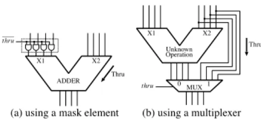
In our approach, for a data path, as many test patterns and responses of each hardware element as possible are propagated along existing data path flows in the data path. If test patterns and responses cannot be propagated along existing data path flows, the DFT method appends DFT elements (e.g. masks, multiplexersand bypass registers) to the data path to guarantee that the test patterns and the responses can be propagated along existing data path flows. We first provide a brief explanation of the DFT method.
Consider testing of a combinational hardware element M with two data inputs, x and y, in the data path. To test M, a
thru
Thru
(a) using a mask element (b) using a multiplexer
thru
Thru
ADDER
X1 X2
Unknown Operation
X1 X2
MUX1 0
Figure 4: Examples of realizing thru function. value specified by a test pattern should be fed into x. We prop- agate the value along a path p from a primary input to x. If an operational module M appears on p, the output value of M will depend on the function and the input value(s) of M .
In order to guarantee that the output of M is completely con- trollable by the input port on p, thru function between the input port and the output is added to M . Most of the popular oper- ational modules (e.g. adder) can realize the thru function by using a mask element. The mask element generates a constant which is required to realize the thru function. Figure 4(a) illus- trates an example of such mask element. If we cannot realize the thru function using the mask element, we realize the thru function using a multiplexer as shown in Figure 4(b). In the rest of this paper, we assume that, for every operational mod- ule, thru function can be realized by mask element in order to simplify the discussion.
However, we cannot achieve the fixed-control testability by adding only the thru functions. The thru functions guarantee controllability of a single path. In case of a hardware ele- ment which has two data inputs, a test pattern must be applied to both the inputs simultaneously. Presence of re-convergent paths in a data path can prevent such application of a test pat- tern to a hardware element which has two data inputs. In par- ticular, this can happen if the propagation paths to the two data inputs of a hardware element start from the same primary in- put and have the same sequential depth2. Such re-convergent paths will cause a timing conflict, i.e. two different values are required on a primary input at the same time. In the concept of strong testability [14], such conflicts are resolved by using hold functions of registers where a register originally has a hold function or is augmented with a hold function. However, since use of hold functions of registers spoils fixed-control testabil- ity, we cannot use the hold functions. To resolve such conflicts, in this DFT method, some registers are bypassed by multiplex- ers and bypass registers are added to some signal lines.
In this DFT method, to control the thru functions, the mul- tiplexers and the bypass registers, additional control inputs are appended as shown in Figure 2.
The goal of the DFT method is to make a given data path fixed-control testable with the minimum hardware overhead. Practical implementation of an algorithm for the DFT method also dictates that the computation time for the DFT insertion and test plan generation algorithms be manageable. We next describe a heuristic algorithm for the DFT method.
Procedure of DFT method
The heuristic algorithm for the DFT proceeds in the follow- ing three steps.
(Step 1) Construct a control forest: To determine paths to prop- agate any pattern, we construct a control forest. The control
2The number of registers on a path is called sequential depth of the path.
X1 X2 X1 X2 X1 X2 X1 X2
PI1 PI2
m10 m9
MULT2 SUB1
MULT1 ADD1
0 1
m5 m4 0 1
0
1 m6 1 0 m8
0 1
m1 m2 0 1
0 m11 1
LAT1
l1 REG1
LAT2
l2 REG2 l4 REG4
REG5 l5
0 m7 1
0 1 1 0
one one
PO1 PO2
0 1 m3
REG3 one
l3
MUX6
MUX3 MUX5
MUX1
MUX8 MUX7
MUX10
MUX2 MUX4
MUX9 MUX11
Figure 5: An example of a data path.
X1 X2 X1 X2 X1 X2 X1 X2
PI1 PI2
m10 m9
MULT2 SUB1
MULT1 ADD1
0 1
m5 m4 0 1
0
1 m6 1 0 m8
0 1
m1 m2 0 1
0 m11 1
LAT1
l1 REG1
LAT2
l2 REG2 l4 REG4
REG5 l5
0 m7 1
0 1 1 0
one one
PO1 PO2
0 1 m3
REG3 one
l3
Control path Propagation input
MUX6
MUX3 MUX5
MUX1
MUX8 MUX7
MUX10
MUX2 MUX4
MUX9 MUX11
Figure 6: An example of a control forest.
forest is a spanning out-forest3of the data path where primary inputs are roots, and its paths are used to propagate test pat- terns.
(Step 2): Construct an observation forest: To determine paths to propagate any response, we construct an observation for- est. The observation forest is a spanning in-forest4of the data path where primary outputs are roots, and its paths are used to propagate responses.
(Step 3) Add DFT elements: To make the data path fixed- control testable, we add DFT elements (extra logic for thru function, multiplexer and bypass register) to the data path at strategic locations.
Details of the algorithm are the following. Step 1: Construct a control forest
A path used for propagating test patterns, from a primary input to a data input of a hardware element, is called a control path to the data input. To reduce the hard- ware of DFT elements which will be added at the third step, the control path should be carefully chosen among all the paths from primary inputs to the data input. In our method, to keep the number of added mask elements where a mask element realizes thru function as small as
3A directed forest in which each data input is reachable from some primary input.
4A directed forest in which there is path from each data output to some primary output.
X1 X2 X1 X2 X1 X2 X1 X2
PI1 PI2
m10 m9
MULT2 SUB1
MULT1 ADD1
0 1
m5 m4 0 1
0
1 m6 1 0 m8
0 1
m1 m2 0 1
0 m11 1
LAT1
l1 REG1
LAT2
l2 REG2 l4 REG4
REG5 l5
0 m7 1
0 1 1 0
one one
PO1 PO2
0 1 m3
REG3 one
l3
Observation path Junction input
MUX6
MUX3 MUX5
MUX1
MUX8 MUX7
MUX10
MUX2 MUX4
MUX9 MUX11
Figure 7: An example of a observation forest.
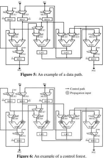
possible, we choose the control paths for each data in- put such that collection of all the chosen paths form an out-forest of the data path. This choice guarantees that a mask element is added to only one of the data input of each two-input operational module. We call the resulting out-forest a control forest. Since the smaller sequential depth intuitively contributes to reduce the test application time, we also pay attention to the the sequential depth of the path while choosing a path. Thus, we construct the control forest as a shortest5spanning out-forest of the data path. Here, for each two-input operational module M, we call one of the data input which is not a leaf of the control forest a propagation input of M and the other not-propagation inputof M.
Let us consider the data path of Paulin[12] shown in Fig- ure 5. We show an example of control forest of the data path in Figure 6. Propagation inputs of the example are X2s of the adder ADD1, the multiplier MULT1 and the subtracter SUB1, and X1 of the multiplier MULT2. Step 2: Construct an observation forest
A path used for propagating any response of a hardware element from its data output to a primary output is called an observation path of the data output. In the observa- tion path, we utilize control paths as much as possible because control paths have the capabilities of propagating any pattern. However, in most case, there exist no control path from the data output port of a hardware element to a primary output. In such a case, we construct an observa- tion path by connecting the minimum number of control paths. If there exist several observation paths each con- sisting of a minimum number of control paths, we choose an observation path such that the collection of all chosen observation paths for all data outputs in the data path form an in-forest. We call the in-forest an observation forest. Here, for each two-input operational module M, if its not- propagation input is on the observation forest, we call the non-propagation input a junction input. If M has a junc- tion input and no thru function between the junction input and its data output, thru function may be added to M to propagate any response from the junction input to the data output. Therefore, we construct the observation forest as
5Any path from a primary input to a data input in the forest is shortest in terms of the sequential depth among all the paths from primary inputs to the port.
a shortest6spanning in-forest of the data path concerned with the number of the not-propagation inputs.
We show an example of observation forest of the data path of Paulin in Figure 7. Junction inputs of the example is X1s of ADD1 and MULT1 and X2 of MULT2.
Step 3: Add DFT elements
DFT elements are added by the following three steps so that test patterns and responses can be propagated along the control paths and observation paths, respectively. Step 3.1: Add thru function to some functional modules on
control paths
For each operational module M, if there exist no thru function between its propagation input and its data out- put, we augment M with thru function between them by adding mask element on its not-propagation input. Step 3.2: Add multiplexers and bypass registers on control
paths
In the step 3.1, it guarantees that any pattern can be prop- agated from a primary input to a data input via a single control path. However, for each two-input operational module M, two patterns must be propagated from pri- mary input(s) to both two data inputs of M by way of two control paths simultaneously. If these control paths are from the same primary input PI and have the same se- quential depth, such re-convergent paths will cause a tim- ing conflict. An example of such re-convergent paths are
PI1 MUX5 REG5 ADD1 MUX3 REG3
MUX6 and PI1 MUX5 REG5 ADD1 MUX1
REG1 MUX6 of Figure 6. To resolve such conflicts, we add a multiplexer or bypass register to one of these paths in the following two cases. Here, let M be the fanout ele- ment in the re-convergent paths and let p be the path from the data output of M to propagation input of M on the control path from PI to the propagation input. Let d be the sequential depth of p.
d 0
If a register on p can be bypassed by adding a multi- plexer, the sequential depth of p becomes d 1 and thus timing conflict can be resolved. Since such by- passing a register may cause a combinational cycle, the connection of the multiplexer should be care- fully determined. Let R be a register which is the nearest to data output of M on p. We insert the mul- tiplexer to the signal line just after the data output of R. If there exists registers on the control paths be- tween PI and M , the data input, which is not on p, of the inserted multiplexer is connected to the data output of the register which is the nearest to M among these registers. Otherwise, the data input is connected to PI. This way of connection makes no combinational cycle. Consider testing of the mul- tiplexer. For justification of test patterns, although control paths of the multiplexer form re-convergent paths, it is guaranteed that sequential depths of these paths are different from each other. For propagation of responses, since a multiplexer is added to path pwhose end is a propagation input, a observation path for the multiplexer can be constructed without DFT elements. An example of insertion of a mul-
6A path from a data output to a primary output in the forest is shortest if the number of not-propagation inputs on the path is smallest among all paths from the data output to primary outputs.
tiplexer TM is shown in Figure 8. The multiplexer is inserted to the signal line just after the data out- put of REG3 and the right data input is connected to the data output of REG5. To test the multiplexer MUX6, we use TM so that paths PI1 MUX5
REG5 ADD1 MUX1 REG1 MUX6 and
PI1 MUX5 REG5 TM MUX6 are used as control paths of MUX6.
d 0
We insert a bypass register to the signal line just af- ter the data output of M . Testing of the bypass reg- ister is also possible in the way as in step 3.1. Here, we consider the possibility of reusing the DFT el- ements. It is generally conceivable that DFT elements which are nearer to primary input are more reusable than those which are nearer to primary outputs. Therefore, we first process two-input operational module which are nearer to primary input and whose control paths start from the same primary input and have the same sequential depth.
Step 3.3: Add thru function to some functional modules on ob- servation path
If there exist junction inputs on the observation path of M, timing conflicts may occur while propagating any re- sponse from the data output z of M to the primary output using the observation path as follows. Any response can be easily propagated along the control path parts using the thru functions. However, it is more complicated to propagate any response through a junction input j of an operational module Mjon the observation path. If Mjhas a thru function between j and its data output l, any re- sponse can be propagated through j using the thru func- tion. However, if Mjhas no thru function between j and l, any response can not be propagated through j. In this case, we consider use of a constant c which is applied to the propagation input k of Mj by way of the control path of k and realizes thru function between j and l. We call the control path of k the support path of k. This may cause a timing conflict between the support path of k and a control path used for propagating either any pattern to M or a similar constant to a preceding operational module on the observation path. The timing conflict is checked and mask elements are added by the following way. No- tice that operational modules which have junction inputs are considered in the order of the data path flow. Let Mj be the nearest operational module to j on the observation path part between z and j such that Mjhas junction input on the path and thru function between the junction input and its data output can be realized by using the support path of its propagation input. Notice that if such module does not exist, we assume that Mjis M. Let I be a set of primary inputs which are used for propagating test pat- terns from primary inputs in I to M and responses from M to j. We assume that control timing of every primary input of I are determined by the preceding processing. In this situation, no timing conflict occur on the following three conditions.
C1: The primary input which is the start of the support path of k is different from every primary input of I. C2: Although C1 does not hold, control timing of the pri-
mary input for the support path of k is different from
X1 X2 X1 X2 X1 X2 X1 X2
PI1 PI2
m10 m9
th1 th5
MULT2 SUB1
MULT1 ADD1
0 1
m5 m4 0 1
0
1 m6 1 0 m8
0 1
m1 m2 0 1
0 m11 1
LAT1
l1 REG1
LAT2
l2 REG2 l4 REG4
REG5 l5
0 m7 1
0 1 1 0
one one
PO1 PO2
0 1 m3
REG3 one
0 1 tm l3
th4 th3
th2 TM
MUX6
MUX3 MUX5
MUX1
MUX8 MUX7
MUX10
MUX2 MUX4
MUX9 MUX11
Figure 8: An example of a fixed-control testable data path.
the other required control timing for the primary in- put.
C3: Although C1 and C2 do not hold, control timing of the primary input for the support path of k can be changed to control timing which is different from the other required control timing for the primary in- put by using multiplexers or bypass registers added at the above steps on the support path or the other required control timing for the primary input can be changed by using multiplexers or bypass registers added at the above steps on the observation path part from the data output of Mjto j.
If none of these conditions hold, Mj is augmented with thru function between j and l by adding mask element on k.
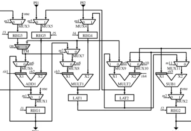
An example of application of the DFT method is shown in Figure 8. In this example, a mask element is added to data inputs X1 and X2 of ADD1, X1 of MULT1, X2 of MULT2 and X1 of SUB1. A multiplexer is added to the signal line just after the register REG3 and the right input of the multiplexer is connected to the data output of the register REG5. Additional control inputs arose to control these DFT elements are th1 to th5 and tm.
5.3 Test Plan Generation for Data Paths Primary and preliminary tests
To test a hardware element M, test vectors for M are prop- agated to the input ports along the control paths of the data inputs of M. If M has two data inputs and is included in a cy- cle in the data path, then the control paths of its data input x may go thru M itself. For example, in Figure 6, the control path of X1 of ADD1 goes thru ADD1 itself. In such a case, a fault of M affect the value propagated thru M and prevent the desired values from reaching x. Thus, we first observe the value propagated through M using the observation path of the data output of M. If the observed value is not the expected one, a fault is detected. We call this test a preliminary test. Notice that we execute the preliminary test for each test vector of M, since affect of a fault depends on the vector value. If no fault is detected in the preliminary test, the test vector is applied to the two data inputs of M and the response of M is observed. We call this test a primary test. However we have to generate
Table 2: Coordinate intersection of C and O.
C
0 1
0 0 1 0
O 1 0 1 1
0 1
= don’t care
Table 3: An example of a test plan.
tPI1 PI2 m1 m2-4 m5 m6 m7-11 l1 l2-4 l5 th1 th2 th3-5 tm PO1 PO2 Phase
1 C - -
2 C 0 0 1 1 1 1 - - Cont.
3 0 0 T 1 1 1 1 1 - - Test
4 0 1 O - Obs.
C : apply test pattern to PI : don’t care O : observe responce at PO - : need not observe T : apply test pattern to control input
test plans for preliminary tests as well as for primary tests, we consider test plan generation for only primary tests. Test plans for preliminary tests can be generated similarly.
Test plans
In the DFT procedure, for each hardware element M, we determine control paths and an observation path of M. In the steps 3.1 and 3.2 of the DFT, we guarantee controllability of the control paths of M by using DFT elements. Similarly, in the step 3.3 of the DFT, we also guarantee observability of the observation path of M and controllability of support paths cor- responding to modules which have junction input on the obser- vation paths with paying attention to timing conflicts between the support paths and the control paths by using DFT elements. Therefore, for testing of M, the collection of the control paths and the support paths can be activated by applying a control vector C to control inputs (including control inputs appended by the DFT) of the data path. Similarly, the collection of the observation path and the support paths can be activated by ap- plying a control vector O to the control inputs.
First, we consider the control sequences of the control phase and the observation phase of the test plan of M. The control se- quence of the control (resp. observation) phase in the test plan of M is composed of only C (resp. O). Consider the lengths of the control sequences of the control phase and the obser- vation phase. Here, let dc and dobe the maximum sequen- tial depth among the control paths and the sequential depth of the observation path, respectively. Let dsbe the maximum sequential depth among paths in the collection of the observa- tion path and the support paths. The length of the control se- quence of the control phase and that of the observation phase are max dc ds do and do, respectively.
Next, we consider the control vector T of test phase in the test plan. The control vector of test phase in the test plan is basically obtained by the intersection of C and O formed from the respective coordinate intersection in Table 2. If M has a control input, since a test pattern corresponding to the control input have to be applied to the control input, it is needed to modify the obtained control vector to a control vector whose coordinate corresponding to the control input is the test pat- tern. The way to apply the test pattern to the control input is presented in the next section.
The test plan is composed of at most three vectors C, T and O. The length of the test plan is max dc ds do do 1.
For example, a test plan of MUX6 of Figure 8 is shown in Table 3.
6. A Method of DFT for RTL Controller/Data
Path Circuits
In this section, we propose a DFT method for a whole cir- cuit which consists of both a controller and a data path. In the DFT method, we adopt our DFT method [4] to the con- troller part and our DFT method proposed in Section 5 to the data path part. In these DFT methods for the controller part and the data path part, we assumed that internal signals, con- trol signals and the status signals, are directly controllable and observable from outside of the circuit. Here, we remove this assumption. The goal of the DFT method proposed in this sec- tion is to provide complete controllability and observability of these internal signals (control and status signals) required for applying test patterns and observing responses.
6.1 Testing of Controllers
For testing of a controller part in a circuit, let us consider to provide complete controllability and observability of status signals and control signals, respectively. It is achieved by ap- pending additional test I/O pins (primary inputs and outputs) and connecting them directly to the status inputs and the con- trol outputs of a controller of the circuit. However, the pin overhead becomes large and it may be unacceptable for practi- cal designs. Instead, the pin overhead is avoided as follows: the status inputs of the controller are directly controlled from pri- mary inputs of the data path by adding a multiplexer “MUX1”, and the control outputs of the controller are directly observed from primary outputs of the data path by adding a multiplexer
“MUX3” as shown in Figure 2. This approach is acceptable be- cause it is generally conceivable that the status inputs (resp. the control outputs) of the controller have smaller bit-width than the primary inputs (resp. the primary outputs) of the data path, and we need not use the data path part at testing of the con- troller. In testing of the controller, these multiplexers “MUX1” and “MUX3” are configured as shown in Table 1.
6.2 Testing of Data Paths
For a data path in a circuit, let us consider a hardware ele- ment M which has data inputs, control inputs, data outputs and status outputs. Each test pattern of M consists of patterns for the data inputs of M and that for the control inputs. We call the former a data input pattern and the latter a control input pattern. Notice that, for testing such a hardware element, we must apply test patterns to both the data inputs and the control inputs. A test plan of M propagates the data input pattern to the data inputs of M from primary inputs. The test plan also applies control input pattern to the control inputs. The test plan also propagates the responses appeared on the data outputs of Mto the primary outputs. The response appeared on the status outputs of M is observable from status outputs of the data path. Control vectors of the test plan of M and the control input patterns for M must be applied to the control inputs (including control inputs appended by the DFT) of the data path. Sim- ilarly, the responses of M must be observed from the status outputs of the data path. If we use additional test I/O pins to make these control inputs and status outputs directly control- lable and observable, respectively, from the outside of the cir- cuit, the pin overhead becomes large. The problem of the pin overhead can be avoided by the following way. Here, we first
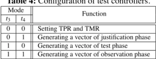
Table 4: Configuration of test controllers.
Mode t3 t4
Function 0 0 Setting TPR and TMR
0 1 Generating a vector of justification phase 1 0 Generating a vector of test phase 1 1 Generating a vector of observation phase
consider the observability of status outputs of the data path. In general, since the bit-width of primary outputs of a controller of the circuit is smaller than that of the status outputs, we can- not use the primary outputs for observing the status outputs. However, the bit-width of the primary outputs of the data path is larger than the status outputs. While testing the data path, it is sufficient to observe the response of a test vector either from primary output or from status outputs. The status outputs and the primary outputs need not to be observed simultaneously. Therefore, we can observe the status outputs using the primary outputs of the data path. In the test architecture of Figure 2, this is achieved by a multiplexer MUX3.
We next consider the controllability of control inputs of the data path. In general, the number of primary inputs of the con- troller is smaller than that of control inputs of the data path. Therefore, we cannot use the primary inputs for applying test plans and control input patterns of hardware elements to the control inputs of the data path. Moreover, in testing of data path, since the primary inputs of the data path are used to ap- ply data input patterns of hardware elements, we cannot use them to apply the test plans and the control input patterns to the control inputs of the data path simultaneously. Therefore, we append an extra circuit called a test controller to generate control input patterns as shown in Figure 2.
Test controller
Test plans are generated for all the combinational hardware elements in a data path of a circuit. In our test architecture shown in Figure 2, all the test plans of the data path are gen- erated by a test controller. The test controller consists of a test plan generator(TP G), a test pattern register(TPR) and a target module register(TMR). Let us consider the testing of a combinational hardware element M, which has data inputs and control inputs, in the data path. The TMR is used to store the index of a test plan either for a preliminary test or a primary test of M. The bit width of the TMR is log2mwhere m is the number of test plans for all the combinational hardware ele- ments in the data path. TheTP Ggenerates the test plan of M if the index of the test plan is stored in the TMR. TheTP G is designed as a combinational circuit and controlled by t3 and t4 as shown in Table 4. TheTP Ggenerates a control vector for a phase of the test plan. The control input pattern of a test pattern for M is pre-stored in the TPR before entering the con- trol phase and is applied to the control inputs by way ofTP G in the test phase. The load enable signal for TPR and TMR is controlled from the t3 and t4 by way of TMR as shown in Table 4. That is, if t3 t4 0 0 is applied, test patterns for control inputs and an index of a test plan is loaded into TPR and TMR from some primary inputs of the data path, other- wise, they hold their values. The mode switching signal t1is used to disable DFT elements of the data path in the normal operation mode of the circuit.
We evaluate hardware overhead ofTP Gs of controller/data path circuits in the next section. Although the hardware over-
head depends on data path designs, for controller/data path cir- cuits dominated data flow, it is conceivable that hardware over- head of theTP Gis low.
We also consider testing of aTP G. Since theTP Gis not used at the normal operation, we test theTP Gonly to confirm that the test plans are generated correctly. It is performed by observing primary outputs of a data path (see Figure 2).
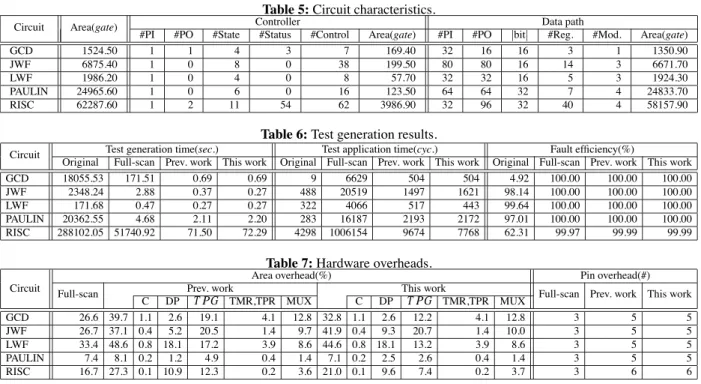
7. Experimental Results
In this section, we evaluate effectiveness of our proposed method by experiments. Circuit characteristics of RTL bench- mark circuits used in the experiments is shown in Table 5. The circuits GCD, JWF, LWF and PAULIN are popularly used ex- amples and the circuit RISC is a practical and large design. In our experiments, we used a logic synthesis tool AutoLogicII (Mentor Graphics) with its sample libraries to synthesize these benchmark circuits. In this table, column “Area” denotes the total areas after synthesis. Here, areas are estimated using gate equivalent of the library cell area. Columns “Controller” and “Data path” denote the characteristics of controller parts and data path parts, respectively: columns “#PI”, “#PO” and
“Area” denote the numbers of primary inputs and primary out- puts and circuit area of respective parts. Columns “#State”,
“#Status” and “#Control” in “Controller” denote the numbers of states, of status inputs and of control outputs. Columns
“ bit ”, “#Reg.” and “#Mod.” in “Data path” denote the bit width of data paths and the numbers of registers and of opera- tional modules in data paths. In the row “RISC”, the number of the status signals is larger than that of the primary inputs of the data path. In our DFT, twenty-two primary output pins are changed to primary input/output pins by appending tri-state buffers. However, the hardware overhead of this modification is negligible.
Test generation results are shown in Table 6. The sequen- tial/combinational ATPG tool TestGen (Synopsis) is used in this experiments on Ultra60 model 2360 (Sun Microsystems). Columns “Test generation time”, “Test application time” and
“Fault efficiency” denote test generation time in second, test application time in clock cycles and fault efficiency. In each of these columns, columns “Original”, “Full-scan”, “Prev. work” and “This work” denote the results of the original circuits (without DFT), of the circuits modified by the full-scan de- sign, of the circuits modified by the method of our previous work[15] and of the circuits modified by our proposed method in this work. Test generation time of the proposed method is almost the same as the method of [15]. Test generation time of the proposed method is shorter than that of the full-scan. Espe- cially, for the circuit RISC, the proposed method can reduce to 1/700 of the full-scan design and can enhance fault efficiency compared with the full-scan design. For the circuit, fault effi- ciency is 99.99% because the combinational ATPG tool can not generate a test pattern for a fault in a multiplier of the circuit in the method of [15] and the proposed method. Test application time of the proposed method is shorter than the method of [15]. Test application time of the proposed method is drastically re- duced compared with that of the full-scan design.
The area and pin overheads of the full-scan design, the method of [15] and the proposed method are shown in Table 7. Columns “C”, “DP”, “TP G”, “TMR,TPR” and “MUX” in columns “Prev. work” and “This work” of column “Area overhead” denote the area overhead of controllers, data paths,
TP Gs, registers TMR and TPR and multiplexers on control signals, status signals and primary outputs of data paths. In the proposed method, area overhead ofTP Gis less compared to the method of [15]. Furthermore, for data paths, however a fixed-control testable data path can achieve simpler test plans compared to strong testable one, the difference between the area overhead of the proposed method and that of the method of [15] is not large. Especially, for RISC, the proposed method can reduce the area overhead compared with the method of [15]. In these results, area overhead of the proposed method is less than that of the method of [15] for all circuits except JWF. The area overhead of the proposed method is larger than that of the full-scan design but the difference between the area over- head of the proposed method and that of the full-scan design is not large. The pin overhead of the proposed method is the same as the method of [15] and larger than that of the full-scan design. For the circuit RISC, the pin overhead of the method of [15] and the proposed method are larger than the other be- cause two select signals for concatenation of two multiplexers are needed on the primary outputs of the data path to observe the control signals and the status signals from the primary out- puts. In return for these disadvantages, the proposed method allows at-speed testing.
In the proposed method, masks, multiplexers and bypass registers are appended to a controller/data path circuit. First, let us consider performance degradation of the circuit caused by multiplexers appended to the controller, the signals between the controller and the data path, and the primary outputs of the data path. Multiplexers are appended in front of the state reg- ister of the controller in the circuit, on control signals between the controller and the data path in the circuit, and in front of the primary outputs of the data path. The multiplexer in front of the state register is the same as the full-scan design. The multiplexer on the control signals does not affect performance of the circuit because the control signals are not generally in- cluded in the critical path of the circuit [11]. The multiplexer in front of the primary outputs of the data path does not also affect performance of the circuit because, in general, there ex- ist registers in front of the primary outputs of the data path and delay of multiplexers are less than operational modules.
For the data path, the performance might be degraded by appended masks, test multiplexers and multiplexers of bypass registers. In the full-scan design, multiplexers are added to all registers to make each register a scannable register. On the other hand, in the method proposed here, masks and multiplex- ers are added to some (not all) operational modules and com- binational paths between two registers, respectively. Further- more, delays of masks is less than that of multiplexers for scan and multiplexers added in the proposed method is the same as multiplexers for scan. Therefore, performance degradation of the proposed method is not so much compared to that of full- scan design.
8. Conclusion
This paper presented a non-scan DFT method for con- troller/data path circuits designed at RTL and that for data path based on fixed-control testability. The proposed method can achieve 100% fault efficiency and allows at-speed testing. We reduced the hardware overhead in the presented method com- pared to the method of our previous work [15]. The hardware