Integrated Test Scheduling, Test Parallelization and TAM Design
Erik Larsson
+∗, Klas Arvidsson
∗, Hideo Fujiwara
+and Zebo Peng
∗Computer Design and Test Laboratory
+Embedded Systems Laboratory
∗Nara Institute of Science and Technology Linköpings Universitet
8916-5 Takayama, Ikoma, Nara 630-0101, Japan SE-582 83 Linköpings, Sweden
{erila, fujiwara}@is.aist-nara.ac.jp {erila, zebpe}@ida.liu.se
Abstract
1We propose a technique integrating test scheduling, scan chain partitioning and test access mechanism (TAM) design minimizing the test time and the TAM routing cost while considering test conflicts and power constraints. Main features of our technique are (1) the flexibility in modelling the systems test behaviour and (2) the support for interconnection test of unwrapped cores and user-defined logic. Experiments using our implementation on several benchmarks and industrial designs demonstrate that it produces high quality solution at low computational cost.
1 Introduction
The testing of System-on-Chip (SOC) designs is a crucial problem mainly due to the increasing design complexity, which leads to high test data volumes. High test data volumes are causing to two major problems depending on each other; (1) how design a minimal test access mechanism (TAM) and (2) how design a test schedule minimizing test time under test conflicts and power constraint.
The work-flow designing an SOC test solution can be divided into two consecutive parts; an early design space exploration followed by an extensive optimization for the final solution. For the former, we have proposed an integrated technique for test scheduling and TAM design minimizing test time and TAM cost [2]. The advantage of the technique is its low computational cost making it useful for iteratively use in the early design space exploration phase. For extensive optimization for the final solution, we have proposed a technique based on Simulated Annealing, which is used only a few times justifying its high computational cost [3]. We have, independently, proposed an integrated test scheduling and scan chain partitioning (test parallelization) technique under power constraints [4].
In this paper, we integrate test scheduling, scan-chain partitioning and TAM design with the objective to minimize test time and TAM routing cost while considering test conflicts and power constraint. An aim is to reduce the gap between the design space exploration and the extensive optimization, i.e. produce a high quality solution in respect
to test time and TAM cost at a low computational cost. We have analyzed our previous approach and noted the TAM design part is of low quality. Further features of our proposed approach are that we support:
• testing of user-defined logic (UDL),
• testing of unwrapped cores,
• memory limitations at test sources,
• bandwidth limitations on test sources and test sinks,
• embedding cores in core.
We have implemented our technique and performed several experiments on benchmarks including a large Ericsson design with 170 tests. Our tool and its modelling are made general, which is an advantage since it can be used to model the test behavior of not only scan tested systems.
The organization of the paper is as follows. An overview of related work is in Section 2 and the considered test arguments are discussed in Section 3. The system model is described in Section 4 and our integrated test scheduling, test parallelization and TAM design technique is presented in Section 5. The paper is concluded with experimental results in Section 6 and conclusions in Section 7.
2 Related Work
In order to minimize the test application time, it is desirable to schedule the tests as concurrent as possible, however, constraints and limitations must be considered. For instance, only one test can be applied at a time to each testable unit and power constraints must be carefully considered otherwise the system can be damaged.
Several test scheduling approaches have been proposed [5,1,6,7]. All are minimizing the test time but taking different issues into consideration. For instance, Chakrabarty proposed a test scheduling technique for core- based systems considering external and BIST test conflicts [5]. The technique proposed by Zorian minimizes the number of control lines for BIST (Built-In Self-Test) systems under power constraint [1]. The test conflicts in such systems are few due to that each testable unit has its dedicated test resources. For general systems, Chou et al. [6] and Muresan et al. [7] have proposed techniques to minimize test time under power limitations and conflicts. An approach designing the TAM and scheduling the tests is proposed by Cota et al. [14].
1. This work has been supported by the Japan Society of Promo- tion of Science (JSPS) under grant P01735 and the Swedish Agency for Innovation Systems (Vinnova).
IEEE the 11th Asian Test Symposium (ATS'02), pp. 397-404, Nov. 2002.
3 Test Arguments
3.1 Test Power Consumption
The power consumption during testing is usually higher compared to normal operation due to that high activity is desired in testing to activate as many faults as possible and minimizing the test time. Chou et al. [6] introduced a test power model by denoting a fixed test power value to each test set. Zorian [1] and Muresan et al. [7] have used the assumption. We will also use it in our approach.
3.2 Scan-chain partitioning
The test time for scan tested cores depends on the number of assigned TAM wires. If a single TAM wire is assigned to a core, all scan chains are formed into a single chain and the test time becomes high. On the other hand, if a high number of TAM wires are assigneed, the scan-chains at the core are distributed over the TAM wires and the test time is reduced.
The test power depends on the activity in the system and by disabling the scan-chains the test power can be reduced [10]. Consider an example of a core with n scan chains. If n TAM wires are assigned, all n chains are active at the same time. The test time is low but the test power consumption becomes high. On the other hand, if a single TAM wire is assigned to the core, all chains are forming a single chain, which results in a high test time. The test power consumption can be the same as in the case with several TAMs since all flip-flops in the scan chains are active. However, each of the scan chains can be loaded one at a time and that reduces the activity to 1/n [10].
3.3 Test Resource Limitations
A test source usually has a limited bandwidth. For instance, an external tester may only support a limited number of scan chains at a time [9]. The memory limitation at a test source may also put a limitation on the testing [9] and there could also be a limitation in number of available pins. 3.4 Interconnection Test
Interconnection test is used to test interconnection between cores as well as UDL placed between cores. An example of an interconnection test is illustrated in Figure 1. The test vectors are transported from the test source r1 to the wrapped core c1using the TAM. The wrapper at c1is put in external test mode in order to perform interconnection test and the UDL, b31, is receiving the test vector. The test response is captured at the wrapper (also in external mode) at core c2. In this example, a TAM is required connecting the test source r1and core c1and from core c2connecting test sink s1. Surrounding cores and UDL blocks such as b32 in this example could interfere during an interconnection test. If so, b31and b32cannot be tested concurrently.
4 System Modelling
In this section, we describe our system model and the input
specification to our test design tool. We illustrate the modelling and the input specification using an example. We also describe the TAM style we are assuming.
We make two observations regarding the cores in a core based environment, there is no specification:
1. given when a UDL block becomes a core, 2. saying a core must be placed in a wrapper.
In our system modelling, we assume that all parts to be tested can be partitioned into cores where some cores are placed in wrappers while other cores are not, wrapped and unwrapped. It means that the UDL blocks are seen as cores that are not placed in wrappers, i.e. they are unwrapped.
A system with a tests method for each testable part could results in a system as in Figure 1. We model such a system by extending our previous system model [2]: design with test, DT = (C, B, T, Rsource, Rsink, pmax, source, sink), where: C= {c1, c2,..., cn} is a finite set of cores; each core, ci∈C, is characterized by:
(xi, yi): placement denoted by x and y coordinates and each core consists of a finite set of blocks ci={bi1, bi2,..., bim} where m>0. Each block, bij∈B, is characterized by:
minbwij: minimal TAM bandwidth, maxbwij: maximal TAM bandwidth.
Each block, bij, is attached with a finite set of tests, bij={tij1, tij2,..., tijk} and each test, tijk∈T, is characterized by:
τijk: test time, pijk: test power,
memijk: required memory for test pattern storage. clijk: constraint list with blocks required for the test. Rsource= {r1, r2,..., rp} is a finite set of test sources where
Figure 1. Modelling the example system. System wrapper
core 1 (c1)
On-chip test generator test source, r2
scan-chain 1
External test evaluator test sink, s1
block 1 (b11)
vbw1 rbw1
vbw2 rbw2
core 3(c3) block 1 (b31)
block 2(b32)
wrapper core2(c2) scan-chain2 block2(b22)
scan-chain1
block1(b21) scan-chain3 scan-chain1 scan-chain2 scan-chain3 scan-chain4
bw21 bw22
External test generator test source, r1
On-chip test evaluator test sink, s2
each test source, ri∈Rsource, is characterized by: (xi, yi): placement denoted by x and y coordinates, vbwi: vector bandwidth,
vmemi: size of vector memory.
Rsink= {s1, s2,..., sq} is a finite set of test sinks; where each test sink, si∈Rsink, is characterized by:
(xi, yi): placement denoted by x and y coordinates, rbwi: response bandwidth,
source: T→Rsourcedefines the test sources for the tests; sink: T→Rsinkdefines the test sinks for the tests; pmax: maximal allowed power at any time;
The input specification for the example system (Figure 1) to our test design tool is outlined in Figure 2. The maximal allowed power limit is given under [Global Constraints] and at [Cores] the placement (x,y) and the blocks at each core are specified. The placement (x,y) of each test source, its possible bandwidth, and available memory are given at [Generators]. At [Evaluators], the placement (x,y) and the maximal allowed bandwidth for each test sink is given. For each of the tests the following is specified under [Tests], the test name, test power, test time, test source (test pattern generator), test sink (test response evaluator), minimal and maximal bandwidth, memory requirement and optional interconnection test with another core. For instance, test t2 is an interconnection test between core c1 and core c2 (Figure 2). The tests for each block are specified at [Blocks] and under [Constraints], the blocks required in order to apply a test are listed. Note, the possibility to specify idle power for each block, which is implemented but to simplify the discussion it is excluded from the system model above. The advantages of this model are that we can model a system with wide range tests (scan tests and non-scan tests such as delay, timing and cross-talk tests) and constraints, for instance we can model:
• interconnection test for UDL (unwrapped cores),
• any combination of test resources, for instance a test source can be on-chip while the test sink is off-chip and vice versa,
• any number of tests per block (testable unit),
• memory requirements at test sources,
• bandwidth limitations at test resources,
• constraints among blocks, which allows modelling of constraints such as cores embedded in cores.
Initially, no TAM exists in the system. Our technique adds a set of TAMs, tam1, tam2,..., tamnwhere each tamiis a set of wires with bandwidth ni. We assume that we can partition the TAM connected to a set of cores freely, which means we are not limited to assigning all wires in a TAM to one core at a time or dedicate TAM wires to a single core.
The TAM is modelled as a directed graph, G=(N, A), where a node ni in N corresponds to a member of C or Rsourceor Rsink. An arc, aij∈A, between two nodes niand nj indicate the existence of a wire and a wire wkis a set of arcs, for instance a wire wkfrom c1to c3passing c2is given by the two arcs: {a12, a23}.
To model the assignment of cores to TAM wires connecting a test source, nsource, a set of cores, n1, n2,..., nn, and a test sink, nsink, we use:
where [] indicates that the nodes (cores) are included (assigned) in this TAM but not ordered.
The length, lj, of a test wire, wj, is given by:
where ni=nsourceand nl=nsink and the function adist gives the absolute distance between two nodes, i.e:
A set of wires form a tamiand the routing cost is:
and the total TAM routing cost in the system is given by:
The total cost for a test solution is given by: α×test time+β×ctam where test time is the total test application time, ctam(defined above) is the total wiring cost, and α and β are designer specified constants determining the relative importance of the test time and the TAM cost.
5 Our Approach
In this section we describe our approach to integrate test scheduling, scan-chain partitioning and TAM design. For a Figure 2. Test specification of the system in Figure 1.
# Example design [Global Constraints] MaxPower = 25
[Cores] name x y {block1, block2,..., block n} c1 10 30 {b11}
c2 10 20 {b21, b22} c3 20 30 {b31, b32}
[Generators] name x y maxbw memory
r1 10 40 3 100
r2 10 10 1 100
[Evaluators] name x y maxbw s1 20 40 4 s2 20 10 4
[Tests] name pwr time tpg tre minbw maxbw mem ict
t1 10 15 r1 s1 1 2 10 no
t2 5 10 r1 s2 2 4 5 c2
// for all tests in similar way
t12 15 20 r1 s2 2 2 2 no
[Blocks] #Syntax: name idle pwr {test1, test2,..., test n} b11 1 {t1, t2, t3} b21 1 {t4, t5} // for all blocks in similar way
b32 2 {t11, t12} [Constraints] Syntax: test {block1, block2,..., block n}
t1 {b11}
t2 {b11, b21, b22, b31, b32} // constraint for all tests in similar way
t12 {b11}
ns our ce→[n1,n2,… n, n]→nsink 1
adist n( i,n1) adist n( k–1,nk)+adist n( n,nl)
k=2 n
+ 2
adist n( i,nj) = xi–xj + yi–yj 3
tamlengthi = li×bandwidthi 4
ct am tamlengthi
∀i n
= 5
given floor-planned system with tests, modelled as in Section 4, we have to:
• determine the start time for all tests,
• determine the bandwidth for each test,
• assign each test to TAM wires,
• determine the number of TAMs,
• determine the bandwidth of each TAM, and
• route each TAM,
while minimizing the test time and the TAM cost considering constraints and power limitations. Compared to our previous approach [2,3,4] the following summarizes the improvements:
• Test scheduling. In [2] when a test was selected and all constraints were satisfied, a TAM was designed. The approach always minimized test time at the expense of the TAM cost. In this approach, a cost function includ- ing test time and TAM cost guides our algorithm.
• Scan chain partitioning (test parallelization). In [4] we maximized the bandwidth for each test, which resulted in a low test time, however, the draw-back is a higher TAM cost. Now, a cost function guides our algorithm.
• TAM design. In [2] when a test was selected and a free TAM existed, it was selected. If an extension was required, an extension was made minimizing the addi- tional TAM. A disadvantage of the approach is illus- trated in Figure 3 where a test D is to be connected using the dashed line. A re-routing as A,C,D,B would include D at no additional cost.
The cost function guiding our algorithm is: :
where: tijkis a test using tamland tamlengthlis the cost of the tam wiring (Eq. 4),τstart: is the time when tijkcan start, and the designer specified factors ftamand ftimeare used to set the relative importance between test time and TAM cost. 5.1 Bandwidth Assignment
Scan chain partitioning allows a flexible bandwidth assignment for each test depending on the bandwidth limitations at the block under test and the bandwidth limitations at the test resources.
The test time (see Section 3.2) for a test tijkat block bijat core ciis given by:
and the test power:
where bwijis the bandwidth [4].
Note, that the test times can often be determined very precisely, however, other issues such as power consumption
is not given at such accuracy; justifying our estimations. Combining the TAM cost and the test time (Equation 7), we get for each block bijand its tests tijk:
where: and k is the
index of all tests at the block. To find the minimum cost of Equation 9, the derivative in respect to bw. Naturally, when selecting the bwij, we also consider the bandwidth limitations at each block.
5.2 Test scheduling
Our test scheduling algorithm is outlined in Figure 4. First, the bandwidth is determined for all blocks (Section 5.1) and the tests are sorted based on a key (time, power or time×power). The outmost loop terminates when all tests are scheduled. In the inner loop, the first test is picked and after calling the create tamplan (Section 5.3) and based on the cost function a TAM is selected or designed for the test. If the TAM factor is important, a test can be delayed in order to use an existing TAM. If all constraints are satisfied, the test is scheduled and the TAM assignment is executed. Finally, all TAMs are optimized.
5.3 TAM Planning
In the TAM planning phase, we:
• create the TAMs,
• determine the bandwidth of each TAM,
• assign tests to the TAMs, and
• determine the start time for each test.
The difference compared to our previous approach is that in the planning phase we only determine the existence of the TAMs but not their routing.
For a selected test, the cost function is used (create tamplan(τ' , test) Figure 5) and if a test is to be scheduled, the time (τ’) when the test is to start and its TAM are determined. If all constraints are satisfied, the TAM plan is determined (execute (tamplan)) (Figure 6).
To compute the cost of extending a TAM wire with a node, the length of required additional wire length is computed. Since the order on a TAM is not decided, we need an estimation technique and for most TAMs, the
Figure 3. Illustration of our previous TAM design. C
A
D
B
c = ftam×tamlengthl+fti me×τs tart 6
τ′ijk = τi jk⁄bwi j 7
p′ij k = pi jk×bwij 8
t b( ij) ll bwi j ftam τijk⁄(bwij)×f
t ime
× +
×
∀k
=
cos 9
ll = [source t( i jk)→ci→sink t( i jk)]
Figure 4. Test scheduling algorithm. for all blocks bandwidth = bandwidth(block)
sort the tests descending based on time, power or time×power τ=0
until all tests are scheduled until a test is scheduled
tamplan = create tamplan(τ, test) // see Figure 5 // τ'=τ +delay(tamplan)
if all constraints are satisfied schedule(τ' )
execute(tam plan) // see Figure 6 // remove test from list
τ = first time the next test can be scheduled order (tam) // see Figure 8 //
largest contribution comes from connecting the nodes at the largest distance from each other. The rest of the nodes can be added on the TAM at a limited additional cost (extra routing). However, for TAMs with a high number of nodes, the number of nodes becomes important. Our estimation of the wire length considers both cases.
1. The nodes N (test sources, test sinks and cores) are evenly distributed over the area, i.e. A = width×height
= (Nx×∆)×(Ny×∆) = Nx×Ny×∆2where Nxand Nyare the number of cores on the x and y axis, respectively:
2. The estimated length, eli, of a wire, wi, with k nodes is:
It means that we compute the maximum between the length as the longest created wire and the sum of the average distances for all needed arcs (wire parts). An example, let nfurthestbe the node creating the longest wire, and nnewthe node to be added, the estimated wiring length after inserting nnewis given by (Eq. 11):
For a TAM, the extension is given as the summation of all extensions of the wires included in the TAM that are needed in order to achieve required bandwidth. The TAM selection for a test tijkis based on the TAM with the lowest cost according to:
Using this cost function, we get a trade-off between
adding a new TAM and delaying a test on an existing TAM. For a newly created TAM, the delay for a test is 0 (since no other test is scheduled on the TAM and the test can start at time 0):
5.4 Example
The TAM assignment is illustrated using an example with four blocks (testable units) placed as in Figure 7(a) and one test per block; the test time is attached to each block. In the example, all tests use the same test resources and no bandwidth limitations exists. Assuming an initial sorting based on test time, i.e. A, D, B, C and success for the schedule at first attempt for each test and the cost function uses ftam:ftimeset to 3:1 in Figure 7 (b) and to 3:2 in (c).
The design flow for the TAM design is illustrated in Table 1. In step 1, A is selected; no TAM exists in the design and the cost for a new to be created is 90, which comes from the distance between TG→A→SA times the tam factor (3). It is a new tam, which means there is no delay for the test; it is scheduled at time 0 to 50. In the second step for D, the TAM created in step 1 can be extended or a new TAM can be created. Both options are estimated. The cost of a new TAM, TG→A→SA, is 150 while the cost of an extension of T1, TG→[A,D]→SA, is 110, computed as TAM extension 20×3 and delay on TAM 50×1. The delay on the TAM is due to that A occupies the TAM during 0 to 50.
5.5 TAM Optimization
Above we created the TAMs for the system, assigned each test to a TAM and determined the bandwidth. In this section, we determine the routing of each of the TAMs, order(tam) (Figure 4) and it is based on a simplification of an algorithm presented by Caseau and Laburthe [13]. The notation TG→[A,D]→SA was used to indicated that core A and D were assigned to the same TAM, however, the order in [A,D] was not determined (Equation 1), which is the objective in this section. We use:
to model that a TAM from nsourceto nsinkconnects the cores in the order nsource, n1, n2,..., nn, nsink.
∆ = A N⁄ x×Ny 10
eli = max1≤ ≤j k{l n( s ource→nj→nsink) ∆, ×(k+1)} 11
el′i max min
l n( s ource→nnew→nf ur thes t→nsink)
l n( s ource→nfur thes t→nne w→nsink)
∆×(k+2)
=
el′i–eli
( )×ftam+delay tam( l,tijk)×ftim e.
= 12
Figure 5. TAM estimation, i.e. create tamplan(τ, test). for all tams connecting the test source and test sink used by the test, select the one with lowest total cost
tam cost=0;
demanded bandwidth=bandwidth(test) if bandwidth(test)>max bandwidth selected tam
demanded bandwidth=max bandwidth(tam)
tam cost=tam cost+cost for increasing bandwith of tam; time=first free time(demanded bandwidth)
sort tams ascending according to extension (τ, test) while more demanded bandwidth
tam=next tam wire in this tam;
tam cost=tam cost+cost(bus,demanded bandwidth) update demanded bandwidth accordingly; total cost=costfunction(tam cost, time, test);
Figure 6. TAM modifications based on create tamplan (Figure 5), i.e. execute (tamplan).
demanded bandwith = bandwidth(test)
if bandwidth(test)>max bandwidth selected virtual tam add a new tam with the exceeding bandwidth decrease demanded bandwidth accordingly
time=first time the demanded bandwith is free sufficient long sort tams in the tam ascending on extension (test)
while more demanded bandwidth tam=next tam in this tam;
use the tam by adding node(test) to it, and make it busy update demanded bandwidth accordingly;
newcost t( i jk) = l source t( ( )j →ci→sink t( )j )×ftam. Figure 7. Example.
x y
10 0
C10
20
0 10 30
(b) Results with ftam:ftimefactor 3:1. (a) Example before TAM design.
D10
TG A50 B10 SA
(c) Results with ftam:ftimefactor 3:2
C10 D10
TG A50 B10 SA
C10 D10
TG A50 B10 SA
ns our ce→n1→n2…→nn→nsink 13
The TAM routing algorithm is outlined in Figure 8. The algorithm is applied for each of the TAMs and initially in each case, the nodes (test sources, cores, and test sinks) on a TAM are sorted descending according to:
where the function dist gives the distance between two cores, or a test source to a core, or a core to a test sink, i.e:
First the test source and the test sink are connected (Figure 8). In the loop over the list of nodes to be connected, each node is removed and added to the final list where the extension is least according to:
where source≤i<sink
We use the TAM, TG→[C,D,A,B]→SA, from the example in Figure 7(a) to illustrate the algorithm, see Table 2. At step 0, the nodes are ordered, C,D,A,B, and a connection is added between TG and SA. At step 1, in the loop over the sorted list, C is picked and inserted between TG and SA and the TAM is modified accordingly. At step 2, D is inserted satisfying Eq. 16. The algorithm continues until all nodes are removed, resulting in a TAM:
TG→A→C→D→Β→SA.
5.6 Complexity
The worst case complexity for the test scheduling when the TAM design is excluded, is of O(|T|3) where T is the set of tests. For the TAM design there are two steps; assignment and ordering. The assignment can be done in: O(|T|×log(|T|)) and the optimization O(|n|2) for a TAM with n cores. However, the optimization is performed after the assignment and the complexity of the test scheduling,
O(|T|3), and the tam design assignment, O(|T|×log(|T|)), gives a total complexity of O(|T|4×log(|T|)).
6 Experimental Results
We have implemented our technique and made a comparison with previously proposed approaches using the Ericsson [3], System L [2], System S [12], ASIC Z [1], an extended version of ASIC Z, and Muresan [7]. All benchmarks are also to be found at [8].
When referring to our technique, unless stated, the reported results are from using sorting based on an initial sorting of the test based on the key: t×p and our previous techniques are referred to as SA (Simulated Annealing) [3] and DATE [2]. For our approach a factor (ftam:ftime) is given to guide our algorithm depending on the importance of test time and TAM cost (see Section 5). The final cost of a test solution is evaluated using: α×test time+β×TAM cost where α and β are designer specified constants determining the relative importance of the test time and the TAM cost (we use α=1 and β=1 unless stated). SA also uses the function. For the experiments we have used a Pentium II 350 MHz processor with 128 Mb RAM. Our previous results referred to as DATE [2] and SA [3] were performed on a Sun Ultra Sparc 10 with 450 MHz processor and 256 Mb RAM [2,3]. To simplify the comparison we assume the two to be equal. 6.1 Test Scheduling
We have made experiments comparing our test scheduling technique with previously proposed techniques, Table 3. For instance, the optimal solution on design Muresan is 25 time units, which is found by SA after 90 seconds while our technique finds it within 1 second.
6.2 Test Scheduling and TAM design
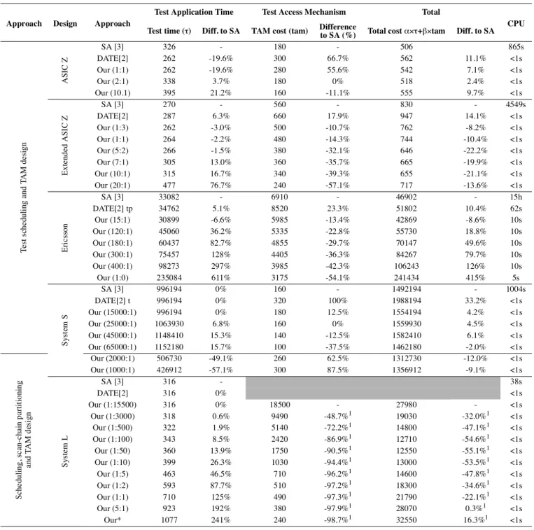
The results on integrated test scheduling and TAM design are collected in Table 4. On ASIC Z when not considering idle power, our technique with (2:1) produces a result 2.4% from the result produced by SA within 1 second while SA required 865 seconds.
Table 1. Illustration of TAM assignment.
Step Test/block Length TAM options Cost Schedule on selected Selected TAM
1 A 50 New:TG→A→SA 30×3+0×1=90 0-50 New:TG→A→SA
2 D 30 New:TG→D→SA
T1:TG→[A,D]→SA
50×3+0×1=150
20×3+50×1=110 0-50-80 T1:TG→[Α,D]→SA,
3 B 10 New:TG→B→SA
T1:TG→[A,D,B]→SA
30×3+0×1=90
0×3+80×1=80 0-50-80 T1:TG→[A,D,B]→SA
4 C 10 New:TG→C→SA
T1:TG→[A,D,B,C]→SA
50×3+0×1=150
0×3+90×1=80 0-50-80 T1:TG→[A,D,B,C]→SA
1 A 50 New:TG→A→SA 30×3+0×2=90 0-50 T1:TG→A→SA
2 D 30 New:TG→D→SA
T1:TG→[A,D]→SA
50×3+0×2=150
20×3+50×2=160 0-30 T2:TG→D→SA
3 B 10
New:TG→B→SA T1:TG→[A,B]→SA T2:TG→[D,B]→SA
30×3+0×2=90 0×3+50×2=100
0×3+30×2=60
0-30-40 T2:TG→[D,B]→SA
4 C 10
New:TG→C→SA T1:TG→[A,C]→SA T2:TG→[D,B,C]→SA
50×3+0×2=150 20×3+50×2=110
0×3+40×2=80
0-30-40-50 T2:TG→[D,B,C]→SA
dist n( s our ce,ni)+dist n( i,nsink) 14
dist n( i,nj) = (xi–xj)2+(yi–yj)2 15
min dist n{ ( i,nnew)+dist n( new,ni+1)–dist n( i,ni+1)} 16 Figure 8. Routing optimization of all TAMs. add test source and test sink to a final list
sort all cores descending according to Eq. 16 while cores left in the list
remove first node from list and insert in the final list insert direct after the position where Eq. 14 is satisfied
For the extended ASIC Z, the total cost using our technique is in the range from 8% to 22% better than SA and the results computed using our technique are made within 1 second compared to 4549 seconds using SA. The results here also demonstrate the improvement regarding the TAM cost using our technique.
For the experiments on the Ericsson design we have used α=1 and β=2. In the previous approaches no bandwidth limitations were given on the external tester [2,3], however, here we assume a bandwidth limitation of 12. Our technique (15:1) produces better results than SA both in respect to test time (6.6%) and TAM (13.4) leading to a total cost 8.6% lower, which was computed after 10 seconds compared to 15 hours of execution for SA. We have made experiments with a variety of ftam:ftimevalues. For instance, experiments neglecting time and only minimizing the TAM (1:0).
For System S, we have used α=1 and β=3100 and in our previous approach we assumed that the external tester supported several tests at the same time [3]. For our approach, we assume that the external tester can support 2 tests concurrently, i.e. more limitation. The optimal test time is found by SA, DATE and our (15000:1). As the ratio ftam:ftimechanges the TAM cost is reduced while the test time show a modest increased leading to a lower total cost. 6.3 Scheduling, Parallelization and TAM design We have performed experiments combining test scheduling, TAM design and test parallelization, Table 4.
For System S (α=1 and β=3100) we have made two experiments combining test scheduling, test parallelization and TAM design where the results indicate the usefulness (cost reduction in the range from 9% to 12%).
For System L we have used α=1 and β=30 and our approach finds the optimal test time, which is also found by SA and DATE. However, the results using SA and DATE do not support TAM of higher bandwidth than 1 and therefore only test time is reported (the experiments were performed ignoring TAM design). In Our* we have forced the bandwidth to 1. The lowest total cost is found for Our (1:50). For the test time and TAM cost, when the former increases, the latter decreases, which is expected.
7 Conclusions
Test time minimization and efficient TAM design is becoming important due to the increasing amount of test data to be transported in a SOC design. We have proposed an integrated technique for test scheduling, scan chain partitioning and TAM design, which minimizes test time and TAM cost while considering test conflicts and power limitations. In our approach it is possible to model a variety of tests as well as tests of wrapped cores, unwrapped cores and user-defined logic. We have implemented the technique and made several experiments.
References
[1] Y. Zorian, “A distributed BIST control scheme for complex VLSI devices”, Proc. of VLSI Test Symp., pp. 4-9,April 1993. [2] E. Larsson and Z. Peng, “An Integrated System-On-Chip Test Framework”, Proc. of Design, Automation and Test in Europe Conference, pp 138-144, March 2001.
[3] E. Larsson, Z. Peng and G. Carlsson, “The Design and Optimization of SOC Test Solutions”, Proc. of Int. Conf. on Computer-Aided Design, pp. 523-530, Nov. 2001.
[4] E. Larsson and Z. Peng, “Test Scheduling and Scan-Chain Division Under Power Constraint”, Proc. of Asian Test Symposium (ATS), pp. 259-264, Nov. 2001.
[5] K. Chakrabarty, “Test Scheduling for Core-Based Systems Using Mixed-Integer Linear Programming”, Trans. on CAD of IC and Sys., Vol.19, No.10,pp. 1163-1174, Oct. 2000. [6] R. Chou et al., “Scheduling Tests for VLSI Systems Under
Power Constraints”, Transactions on VLSI Systems, Vol. 5, No. 2, pp. 175-185, June 1997.
[7] V. Muresan et al., “A Comparison of Classical Scheduling Approaches in Power-Constrained Block-Test Scheduling”, Proc. of International Test Conf., pp. 882-891, Oct. 2000. [8] E. Larsson, A. Larsson, and Z. Peng, “Linkoping University
SOC Test Site“, http://www.ida.liu.se/labs/eslab/soctest/ Table 2. Illustration of TAM routing.
Step Selected Order before selection Length of each TAM partition Order after selection TAM length Remaining in list
0 - TG→SA 30 C,D,A,B
1 C TG→SA 0 TG→C→S 14+22=36 D,A,B
2 D TG→C→SA 18,2 TG→C→D→SA 14+10+14=38 A,B
3 A TG→C→D→SA 6,14,20 TG→A→C→D→SA 10+10+10+14=44 B
4 B TG→A→C→D→SA 20,14,14,6 TG→A→C→D→Β→SA 10+10+10+10+10=50 -
Table 3. Test scheduling results. Design Approach Test time Difference
to optimum (%) CPU (s)
Muresan [7]
Optimal 25 - -
SA [3] 25 0 90
Muresan [7] 29 16.0 -
DATE [2] 26 4.0 1
Our (p) 25 0 1
SystemS [12]
Optimal 1152180
Chakrabarty SJF 1204630 4.5 -
DATE [2] 1152180 0 1
Our 1152180 0 1
SystemL [2]
Optimal 1077 - -
DATE [2] 1077 0 1
Our 1077 0 1
Designer 1592 47.8 -
Ericsson [3]
Optimal 30899 - -
SA [3] 30899 0 3260
DATE [2] (t) 34762 12.5% 3
Our 30899 0 5
[9] G. Hetherington et al., “Logic BIST for Large Industrial Designs: Real Issues and Case Studies”, Proc. of International Test Conference. ,pp. 358-367, Sep. 1999. [10] E. Larsson and H. Fujiwara, “Power Constrained Preemptive
TAM Scheduling”, Formal proccedings of ETW, Corfu Greece, May 2002.
[11] M. L. Bushnell and V. D. Agrawal,“Essentials of Electronic Testing for Digital, Memory, and Mixed-Signal VLSI Circuits”,Kluwer Academic Publisher,ISBN 0-7923-7991-8.
[12] K. Chakrabarty, “Test Scheduling for Core-Based Systems”, Proc. of International Conference on Computer Aided Design,page 391-394, San Jose, CA, Nov. 1999.
[13] Y. Caseau and F. Laburthe, “Heuristics for large constrained vehicle routing problems”, Journal of Heuristics, vol.5, no.3, pp. 281-303, October 1999.
[14] E. Cota et al., “Test Planning and Design Space Exploration in a Core-based Environment”, Proceedings of DATE, 2002, pp. 478-485, Paris, France, March 2001.
Table 4. Experimental results on (1)integrated test scheduling and TAM design and on (2) combined test scheduling, TAM design and test parallelization. For results on System L with index 1 we compare with Our (1:15500).
Approach Design Approach
Test Application Time Test Access Mechanism Total
CPU Test time (τ) Diff. to SA TAM cost (tam) Differenceto SA (%) Total costα×τ+β×tam Diff. to SA
TestschedulingandTAMdesign ASICZ
SA [3] 326 - 180 - 506 865s
DATE[2] 262 -19.6% 300 66.7% 562 11.1% <1s
Our (1:1) 262 -19.6% 280 55.6% 542 7.1% <1s
Our (2:1) 338 3.7% 180 0% 518 2.4% <1s
Our (10.1) 395 21.2% 160 -11.1% 555 9.7% <1s
ExtendedASICZ
SA [3] 270 - 560 - 830 - 4549s
DATE[2] 287 6.3% 660 17.9% 947 14.1% <1s
Our (1:3) 262 -3.0% 500 -10.7% 762 -8.2% <1s
Our (1:1) 264 -2.2% 480 -14.3% 744 -10.4% <1s
Our (5:2) 266 -1.5% 380 -32.1% 646 -22.2% <1s
Our (7:1) 305 13.0% 360 -35.7% 665 -19.9% <1s
Our (10:1) 315 16.7% 340 -39.3% 655 -21.1% <1s
Our (20:1) 477 76.7% 240 -57.1% 717 -13.6% <1s
Ericsson
SA [3] 33082 - 6910 - 46902 - 15h
DATE[2] tp 34762 5.1% 8520 23.3% 51802 10.4% 62s
Our (15:1) 30899 -6.6% 5985 -13.4% 42869 -8.6% 10s
Our (120:1) 45060 36.2% 5335 -22.8% 55730 18.8% 10s
Our (180:1) 60437 82.7% 4855 -29.7% 70147 49.6% 10s
Our (300:1) 75457 128% 4405 -36.3% 84267 79.7% 10s
Our (400:1) 98273 297% 3985 -42.3% 106243 126% 10s
Our (1:0) 235084 611% 3175 -54.1% 241434 415% 5s
SystemS
SA [3] 996194 0% 160 - 1492194 - 1004s
DATE[2] t 996194 0% 320 100% 1988194 33.2% <1s
Our (15000:1) 996194 0% 180 12.5% 1554194 4.2% <1s
Our (25000:1) 1063930 6.8% 160 0% 1559930 4.5% <1s
Our (45000:1) 1148410 15.3% 140 -12.5% 1582410 6.1% <1s
Our (65000:1) 1152180 15.7% 100 -37.5% 1462180 -2.0% <1s
Scheduling,scan-chainpartitioning andTAMdesign
Our (2000:1) 506730 -49.1% 260 62.5% 1312730 -12.0% <1s
Our (1000:1) 426912 -57.1% 300 87.5% 1356912 -9.1% <1s
SystemL
SA [3] 316 - 38s
DATE[2] 316 0% <1s
Our (1:15500) 316 0% 18500 - 27980 - <1s
Our (1:3000) 318 0.6% 9490 -48.7%1 19030 -32.0%1 <1s
Our (1:500) 322 1.9% 5140 -72.2%1 14800 -47.1%1 <1s
Our (1:100) 343 8.5% 2420 -86.9%1 12710 -54.6%1 <1s
Our (1:50) 360 13.9% 1750 -90.5%1 12550 -55.1%1 <1s
Our (1:10) 399 26.3% 1030 -94.4%1 13000 -53.5%1 <1s
Our (1:5) 463 46.5% 710 -96.2%1 14600 -47.8%1 <1s
Our (1:2) 593 87.7% 510 -97.2%1 18300 -34.6%1 <1s
Our (1:1) 710 125% 490 -97.3%1 21790 -22.1%1 <1s
Our (5:1) 923 192% 380 -97.9%1 28070 0.3%1 <1s
Our* 1077 241% 240 -98.7%1 32550 16.3%1 <1s