Instruction-Based Delay Fault Self-Testing of Pipelined
Processor Cores
Virendra Singh
1,3, Michiko Inoue
1, Kewal K Saluja
2, Hideo Fujiwara
11
Nara Institute of Science & Technology, Takayama, Ikoma, Nara – 630-0192 Japan
2
University of Wisconsin-Madison, USA
3
Central Electronics Engineering Research Institute, Pilani, India
{virend-s, kounoe, fujiwara}@is.naist.jp, [email protected]
Abstract—Although nearly all modern processors use pipelined architecture, yet no method has been proposed in literature to model these for the purpose of test generation. This paper proposes a graph theoretic model of pipelined processors and develops a systematic approach to delay fault testing of such processor cores using the processor instruction set. Our methodology consists of using a graph model of the pipelined processor, extraction of architectural constraints, classification of paths, and generation of tests using a constrained ATPG. These tests are then converted to a test program, a sequence of instructions, for testing the processor. Thus, the tests generated by our method can be applied in functional mode of operation and can also be used for self-test. We applied our method to two example processors, namely a 16 bit five stage VPRO pipelined processor and a 32 bit pipelined DLX processor, to demonstrate the effectiveness of our methodology.
I.
II.
I
NTRODUCTIONIn modern high performance processors, it is no longer sufficient to target conventional stuck-at faults, instead delay faults and cross talk faults are becoming increasing important. At-speed testing using external tester is almost infeasible because of its inherent accuracy limitation and cost. Due to the need of design change, possibility of excessive power consumption, and high area and performance overhead, hardware-based self-test (BIST) is also not a feasible solution. Software-Based Self-Test (SBST) is an alternate to BIST which uses processor instructions and functionality in order to test processor core in functional mode.
A number of approaches have been proposed for testing non- pipelined processors targeting stuck-at faults but a very few [2,3] approaches have been proposed to test pipelined processors. Chen [2] proposed a template based methodology, whereas Kranitis[3] proposed an approach which targets functional blocks. Though pipelined processors are studied in [2,3], the pipelined behavior is not considered, instead the focus is on functional blocks; and also faults in the controller are not explicitly addressed. Researchers in [4,5,6] proposed SBST approaches targeting delay faults for non- pipelined processors. However, Lai’s [4] approach does not provide details about testing the controller, whereas [5, 6] provide an efficient graph theoretic model based approach, it is also limited to non-pipelined processors, though it can handle architectural registers and an FSM based controller.
The paper is organized as follows. Section II lists the contributions of this paper and describes an overview of our methodology. Section III and IV describe the test generation methods for datapath and controller. Section V describes the instruction sequence generation process. Section VI presents experimental results to demonstrate the effectiveness our methodology, and finally we conclude with section VII
.
C
ONTRIBUIONS ANDO
VERVIEW OF THE PROPOSED APPROACHTo the best of our knowledge, no approach has been proposed in literature for testing pipelined processors and targeting delay faults. We believe this is the first work towards modeling of pipeline behavior for testing of a microprocessor in functional mode.
The main contributions of this work are:
1. Develop a graph theoretic model for pipeline behavior using the RT level description of the processor,
2. Provide a systematic approach to test the processor based on the model.
This paper presents a unified approach to test normal and bypassing/forwarding paths in the datapath by using a graph model of the behavior of the datapath and the controller. A hierarchical approach is presented for the test generation, which classifies paths at RT level and extract constraints for potentially testable paths to generate test vectors at gate level using constrained ATPG. Path delay fault model [7] is used in this work.
Unlike a non-pipelined processor, in which one instruction must finish execution before the execution of the next instruction, in a pipelined processor multiple instructions can be in various stages of execution. This makes its behavior more complex. These stages can be viewed as independent hardware units and all the stages execute instructions concurrently. In order to support concurrent execution of instructions, necessary data and control signals are carried along as an instruction progresses in the pipeline stages. Simultaneous execution of multiple instructions can lead to data, control and structural hazards. Data bypassing is a commonly used technique to resolve data hazards and stalling is used for the unresolved hazards. Data flows from the first pipeline stage to the last pipeline stage during the normal execution (without any hazard). It is very difficult to separate datapath and controller part in a pipelined processor as every pipeline stage carries all the data and control This work was supported in part by Semiconductor Technology
Academic Research Center (STARC) under the Research Project and in part by Japan Society for the Promotion of Science (JSPS) under Grants-in- Aid for Scientific Research B (2) (No. 15300018).
0-7803-8834-8/05/$20.00 ©2005 IEEE. 5686
2005 IEEE International Symposium on Circuits and Systems (ISCAS 2005) , pp.5686-5689, May 2005.
signals required by the pipeline stages ahead of it. Nonetheless, our model defines them clearly, yet for testing the paths in the datapath part and the control part are treated separately. The data transfer activities between the architectural registers and data and address (memory address and register address) part of the pipeline registers are assumed be in the datapath and the remaining paths are considered in the control part.
A graph theoretic model called pipeline instruction execution graph (PIEG), has been developed that is constructed by using instruction set architecture and RT level description. It is based on instruction execution graph (IE-Graph) introduced by us in [5,6], and similar work in [1] for non-pipelined processors. Our present model classifies paths as functionally testable (FTP), functionally untestable (FUTP), potentially functionally testable (PFTP), and parity check functionally untestable (PCFTP). After the classification, it extracts constraints for the PFTP and PCFTP paths. First, constraints on the control signals in one or more relevant pipeline stages are extracted and then the constraints on justifiable data in the data registers or pipeline registers under the control constraints are extracted. PCFTPs are further classified FUTPs or PFTPs. A combinational constrained ATPG is used for the test vector generation for the PFTPs. We can get test sequences without using ATPG for FTPs, and test sequence is not needed for FUTPs. For testing the controller, the constraints on the legitimate values for a group of control signals are extracted by using RT level description. PIEG is used along with these constraints for further extraction of control and data constraints for target control paths, and their classification. Constraint ATPG is used to generate the test vectors. Finally, an instruction sequence to apply the generated test vectors, is generated by using the knowledge of the control signals of various pipeline stages and the PIEG.
III. D
ATAPATHIn this section we consider the paths that are responsible to transfer data between architectural registers or data and address between pipeline registers, which are significant in number. Other paths are considered in the control part. Datapath of a pipelined processor can be modeled by PIEG which captures the pipeline behavior, and is used for constraint extraction, path classification, and instruction sequence generation. Nodes of the PIEG are: (i) registers, (ii) part of registers which can be independently readable and writeable, (iii) equivalent registers (set of registers which behave identically for all instructions, like register file), (iv) two special nodes, IN and OUT, which model the external world such as memory and IO devices, and (v) data and address (memory address and register address) part of pipeline registers. A directed edge is drawn between two nodes iff there exists at least one instruction responsible to transfer data (with or without manipulation) between the corresponding two registers. Each edge is marked with a 4-tuple [<instruction set>, <stage from, stage to>,
<distance>, <logic type>]. This 4-tuple signifies that the instructions from the <instruction set> are responsible for the transfer of data from <stage from> to <stage to> through the logic specified by <logic type>, and the pair of instructions for delay testing must be separated by the number of cycles specified by the
<distance>.Informally, the number of pipeline stages bypassed by a path is referred to as distance.
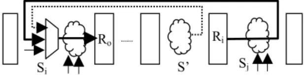
We use our 16 bit, 5 stage pipelined processor VPRO design [9], which has 24 instructions as an example processor to explain the concepts. A partial PIEG of VPRO is shown in Figure 1, and complete PIEG and other details are given in [9].
Logic classification for <logic type> was based on our observation that many paths directly transfer data to the next stage using simple interconnects or through multiplexers. Keeping this in
mind we classified logic into three types, namely interconnect (I), multiplexers (M), and processing logic (L). This classification simplifies the test generation process.
[<I2-21>,<mem,id>,2,M]
[<I2-21>,<ex,id>,1,L]
RF S1 ALO
[<I2-21>,<id,id>,0,M] [<I2-21>,<ex,ex>,0,L]
Instructions, which have identical behavior in a given stage, are defined as equivalent instructions for that stage. For example, ADD and INC are the equivalent instructions in the EX stage of the VPRO processor. We can use these equivalent instructions to reduce the cardinality of the instruction set marked on each edge, which in turn reduce the constraint extraction and test generation effort.
Figure 1 Partial PIEG of VPRO processor
We assume that any instruction can be followed by any other instruction in a pipeline stage with the exception of those instructions, which always need stall after the execution, such as unconditional jumps.
To test a path from a register Ri to a register Ro, we must create a transition at Ri and capture the transferred data at Ro. We need two data transfers to Ri to make a transition at Ri, and one data transfer from Ri to Ro along the target path. Though there may be a bypass/forwarding path (with one or more distance) to Ri, there must be another normal path (zero distance path) which brings the same values as the bypass path, and hence we only consider the normal path for data transfer to Ri. We also allow the propagation of data to Ro through normal paths except from Ri.
In order to generate the test vectors to be applied in functional mode, we need to extract architectural constraints. There are two types of constraints, i) control constraints, ii) data constraints. Control constraints are the constraints on control signals, which are responsible to transfer data between two nodes. These are obtained from PIEG. Data constraints are the constraints on justifiable data under the control constraints.
R
iR
oS
jA path from register Ri to register Ro, marked with [<Iset>,
<Sj, Si>, d, LT], where LT∈{I, M, L}, can be tested by a test instruction sequence IP1, IP2, ID1, ID2, ……I_Dd-2, IS1, and IS2. To test a path we need constraints for both stages Sj and Si in two consecutive cycles (see Fig. 2). Instruction pair IP1, IP2 creates a transition at register Ri and allows it to propagate in Sj stage, hence provide the control constraints for the stage Sj. Instruction pair IS1, IS2 propagates it in Si stage and finally instruction IS2 latches the result in register Ro; hence provide the control constraints for the stage Si. Other instructions ID1, ……IDd-2 are dummy instructions between IP2 and IS1 to excite the path. Though there may be another data from another stage (ex. data from S’ in Fig. 2), we assume that such data is transferred through a MUX and does not affect data transfer along the target path. Therefore, ATPG does not care these values and we do not need to extract their constraints.
S
iS’
Figure 2 Target path and pipeline stages
5687
Control constraints are extracted as instruction pairs (IP1, IP2) and (IS1, IS2). Instruction pair (IP1, IP2) must be marked on any zero distance (d = 0) in-edge of Ri and instruction pair (IS1, IS2) must be marked on the target path (edge between Ri and Ro). Note that IP2
= IS1 if d=1, and IP1 = IS1 and IP2 = IS2 if d=0.
Data Constraints for the three different logic types are extracted as follows:
(1) when logic type is interconnect ‘I’:
These paths are generally used to carry data to the next stage and always have zero distance (d = 0). Ro has only one edge, and that is from Ri; hence, it will not observe any data constraint. These paths can always be tested as interconnects test, therefore they are classified as FTP.
(2) when logic type is multiplexer ‘M’:
These paths pass through a set of MUXs and behave as interconnects if control signals are properly assigned. Therefore, under the control constraints (proper assignment of MUX select signals), data constraints are not applicable, as other paths to Ro
will automatically be disintegrated with the proper assignment of MUXs control signals.
These paths are classified as FUTP if these are marked with d=1 and have a self-loop because a transition cannot be launched. Otherwise, paths are classified as FTP and these paths can be tested as interconnect test.
(3) when logic type is processing logic ‘L’:
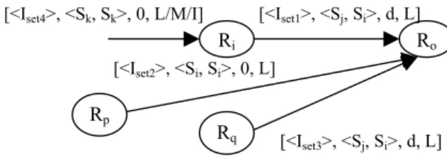
This includes the paths which pass through the combinational logic. Let an edge between two registers Ri and Ro be marked with [<Iset1>, <Sj, Si>, d, L>]. Following edges and registers must be considered: i) All the in-edges to Ro with distance d and logic type
‘L’ (having some instructions common with Iset1), ii) all the in- edges to Ro with zero distance, logic type ‘L’, and have some instruction common with Iset1, iii) all the zero distance (d=0) in- edges to Ri.
All those registers which have out-edge to Ro (with distance d (same as target path distance), logic type ‘L’, and some instruction common with the target path) provide the data constraints for the propagation of created transition in Sj stage. All those registers which have out-edge to Ro (with zero distance, logic type ‘L’, and have some instruction common with the target path) provide data constraints for the propagation of the created transition in Si stage. Figure 3 shows the edges and nodes which are needed to be considered. Note that Iset1∩ Iset2≠ φ, Iset1∩ Iset3≠ φ.
We consider different distance cases separately: when d = 0 (Normal paths inside a pipeline stage):
We have to find out the data constraints for all those registers which have zero distance (d=0) in-edge to Ro with logic type ‘L’ using PIEG and RTL description. Let Ro has an in-edge from register Rp which is marked with common instructions with the target edge.If selected instrcution IS2 is not marked on any of zero distance in-edge of Rp, then Rp must have constant value across two time frames (under IS1 and IS2). Otherwise, the register Rp do not observe any data constraints.
when d = 1 (paths across the pipeline stages, i.e. forwarding paths) (a) Paths from bit ito bit i of register Ri in case of self-loop
These paths can be functionally testable only when there is odd inversion parity exists in the path; otherwise, these paths are functionally untestable. These paths are declared as PFTUP. Many paths of such kind exist in the circuit, such as paths in the pass logic of ALU, paths in shifter, paths in logic operation block of ALU etc.
Constraints must be extracted for the registers which have unity delay edge to Ro under IP1 and IS1 instructions, and for register which has zero distance edge to Ro under IS1 and IS2
instructions, as explained in d = 0 case.
(b) For other cases, paths are PFTP and data constraints can be obtained as stated above.
Similarly, constraints can be obtained for d >1 case. Details are given in [9].
Inversion parity test program is used to further classify PCFTP paths into FUTP or PFTP. The above stated classification can also be used to simplify the circuit for ATPG. Constraint ATPG is used for test vector generation for all the PFTP paths by using extracted constraints.
IV. C
ONTROLLERIn order to execute an instruction, the instruction is decoded by the decode unit (in decode stage) which dispatches control signals along with the required data for the pipeline stages ahead. Therefore, each pipeline stage does have control signals that are not structured in nature but often form a small group. In our approach, small grouping is used to find constraints. Therefore, we need to extract two types of constraints: i) constraints on the legitimate value of the group of control signals, ii) constraints on inter group signals in a pipeline stage.
(i) Constraints on the legitimacy of signals: Every possible value of a small group of signals is not valid. Therefore, we need to extract all the legitimate values. For example, comparator control (comp_ctrl) signals in VPRO are grouped in a group of 3 bits, and legitimate values are <0XX, 10X, and 110>. (ii) Constraints on inter group signals: We extract these
constraints in terms of instructions, i.e., map to the instruction which can generate the particular combination and all possible combinations are extracted. For example, in VPRO when ALU ctrl (alu_ctrl) signal is 0000 the comparator control (comp_ctrl) signal must be 000. Here onwards we will discuss how we can use these constraints for the test generation. The part of a pipeline register, which carries the control signals is called control register. There are paths between control register (CR) to control register, control register to data register (DR), or data register (such as IR) to control register. The paths between CR-to-CR are used to carry the control signals for the pipeline stages ahead. These paths are connected directly and can be tested as interconnects. Paths from CR to DR are the paths which pass through the combinational logic. We construct a table which shows the transition at some bit in CR with instructions after exclusion of equivalent instructions.
[<Iset1>, <Sj, Si>, d, L] [<Iset4>, <Sk, Sk>, 0, L/M/I]
R
iR
o[<Iset2>, <Si, Si>, 0, L]
R
pR
q [<Iset3>, <Sj, Si>, d, L]
Figure 3 Edge consideration for constraint extraction
Let there be a path between a bit i of control register Ci, and data register Ro. Constraints can be extracted in the following manner: (i) when Ci and Ro are in the same stage:
It needs an instruction sequence of two instructions (IS1, IS2). The instruction pairs that can produce a transition at bit i and also marked on the in-edge of the register Ro can be the test instructions (IS1, IS2). All the data registers that have zero distance out edge to Ro (have some common instructions with the selected potential instruction pairs) are needed to check for data constraints. Data constraints can be obtained in the same way as we obtain for datapath.
5688
(ii) when Ci and Ro are in different stages:
Instruction sequence (IP1, IP2, ID1, ……IDd-2, IS1, IS2) is needed to apply test vector. The instructions which can produce the transition at bit i of Ci can act as IP1, IP2. Constraints on the registers which have out-edge to Ro (with distance = d) must be considered under IP1, and IP2. The instructions which are marked on the in-edge of Ro (with distance = d) can act as IS1, IS2, and data constraints on those registers which have zero distance out- edge to Ro must be considered under the control constraints of IS1, IS2 instructions.
V.
VI.
T
EST INSTRUCTION SEQUENCE GENERATION The generated test vector pairs as explained above are assigned to control signals and registers. A sequence of instructions is needed to apply these test vectors. A sequence of instructions which is responsible to launch the transition, propagate the launched transition, and latch the result, provided that desired data are available in the appropriate registers, is called test instruction sequence. These data are made available by the justification instruction sequence. Finally, the result must be transferred to memory by a sequence of instructions called observation sequence. It is clear from the earlier discussion that if an edge between registers Ri and Ro is marked [<Iset>, <Sj, Si>, d, LT], then we need a test instruction sequence (IP1, IP2, ID1, ……IDd-2, IS1, IS2) to apply the test vectors provided that test vectors are available in desired registers. Instructions IP1 (when d > 0) and IP2 (when d > 1) are decided by the control signals of the stage Sj, and instructions IS1 and IS2 are decided by the control signals of Si stage. If there are more than one potential candidates for these instructions then we must select easy to observe instruction (such as STORE) for IS2, and easy to justify instruction for the rest. Once IP1, IP2, IS1, IS2instructions are decided, we fill the rest of the instructions by NOP instructions, but these can be later on replaced by the justification instruction for IS1 and IS2 to reduce the number of instructions.
E
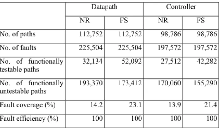
XPERIMENTAL RESULTSVPRO processor was synthesized using 2345 gates and 268 sequential elements, and pipelined DLX processor [8] was synthesized with 34,347 gates and 1898 sequential elements. Complete PIEGs for both the processors are constructed by using instruction set architecture and RT level description. Note that the PIEG is extracted manually in this work but this can be automated.
VII.
PIEG is used for the constraint extraction and the path classification. A constrained ATPG is developed for delay faults as commercially available ATPG doesn’t handle the required constraints. Results for VPRO and DLX processors for the Non Robust (NR) and Functional Sensitizable (FS) [7] tests are shown in the Tables 1 and 2 respectively. Less than 1% paths are classified as PCFTP which are further classified as FUTP. The results show that only a small number (about 24%) of paths are functionally testable. However, we achieve 100% fault efficiency.
C
ONCLUSIONA systematic approach for the delay fault testing of a pipelined processor cores using their instruction set has been presented. A graph theoretical model has been developed to model the complex pipeline behavior. This model can efficiently extract the constraints under which a processor can be tested. This model also assists the test instruction sequence generation process. Some paths can be declared as functionally untestable paths at the early stage. We
would like to extend this model for the more complex processors such as super-scalar architecture in future.
Table 1 Results for VPRO processor
Datapath Controller
NR FS NR FS
No. of paths 112,752 112,752 98,786 98,786
No. of faults 225,504 225,504 197,572 197,572 No. of functionally
testable paths
32,134 52,092 27,512 42,282
No. of functionally untestable paths
193,370 173,412 170,060 155,290
Fault coverage (%) 14.2 23.1 13.9 21.4
Fault efficiency (%) 100 100 100 100
Table 2 Results for pipelined DLX processor
Datapath Controller
NR FS NR FS
No. of paths 372,459 372,459 190,542 190,542
No. of faults 744,918 744,918 381,084 381,084 No. of functionally
testable paths
148,718 185,247 57,502 89,974
No. of functionally untestable paths
596,200 559,671 323,582 291,110
Fault coverage (%) 19.9 24.8 15.0 23.6
Fault efficiency (%) 100 100 100 100
R
EFERENCES[1] S.M. Thatte and J. Abraham, “Test generation for Microprocessors”, IEEE Trans. on Computers, Vol. C-29, No.6, June 1980, pp. 429-441. [2] L. Chen, S. Ravi, A. Raghunath, and S. Dey, “A Scalable Software- Based Self-Test Methodology for Programmable Processors”, Proc. of the Design Automation Conference 2003, pp. 548-553.
[3] N .Kranitis, G. Xenoulis, A. Paschalis, D. Gizopolous, Y. Zorian,
“Application and Analysis of RT-Level Software-Based Self-Testing for Embedded Processor Cores”, Proc. of International Test Conference, 2003, pp 431-440.
[4]. W.-C. Lai, A. Krstic, and K.-T. Cheng, “Test Program Synthesis for Path Delay Faults in Microprocessor Cores”, Proc. of International Test Conference 2000, pp 1080-1089.
[5] V. Singh, M. Inoue, K.K. Saluja, and H. Fujiwara, “Instruction-Based Delay Fault Testing of Processor Cores”, Proc. of the International Conference on VLSI Design 2004, pp 933-938.
[6] V. Singh, M. Inoue, K.K. Saluja, and H. Fujiwara, “Delay Fault Testing of Processor Cores in Functional Mode”, IEICE Trans. on Information & Systems, Vol. E-88D, No. 3, pp 1-9.
[7]. A. Krstic and K.-T. Cheng, Delay fault testing for VLSI circuits, Kluwer Academic Publishers, 1998.
[8] J.L. Hennesy, and D.A. Patterson, Computer Architecture: A Quantitative Approach, Morgan Kaufmann Publishers, 1996. [9] V. Singh, M. Inoue, K.K. Saluja, and H. Fujiwara, “Instruction-Based
Delay Fault Self-Testing of Pipelined Processor Cores”, NAIST Technical report. http://isw3.aist-nara.ac.jp/IS/TechReport/2004006.