On Minimization of Test Application Time for RAS
Abstract—Conventional Random access scan (RAS) for testing has lower test application time, low power dissipation, and low test data volume compared to standard serial scan chain based design. In this paper, we present two cluster based techniques, namely, Serial Input Random Access Scan and Variable Word Length Random Access Scan to reduce test application time even further by exploiting the parallelism among the clusters and performing write operations on multiple bits. Experimental results on benchmarks circuits show on an average 2-3 times speed up in test write time and average 60% reduction in write test data volume compared to conventional Random Access Scan.
Index Terms—Random Access Scan (RAS), Scan Design, DFT 1. INTRODUCTION
Serial scan design has been a standard practice in industry for VLSI testing because of its simplicity and lower area overhead. As the number of flips-flops and gates on a chip, and the complexity of circuit designed is increasing rapidly, testing of these large sequential circuits is becoming increasingly difficult. With increase in number for Scan Flip- flops (SFFs), test application time for testing with serial scan design increases. Test application time, area overhead, and test data volume for DFT, are the major part of the test cost. Due to high cost of ATE, higher test application time results into higher test cost for serial scan DFT. We target to reduce test application time to reduce test cost in this work. In serial scan design higher switching activity takes place in many SFFs, resulting into higher power dissipation during testing. As an alternative to serial scan design, Random Access Scan (RAS) was first proposed by Ando [1] in 1980. However, due to high area overhead and high transistor cost, it was considered as impractical at that time. Since then the transistor cost has been reducing exponentially and test cost has been increasing. In 2004, Baik et al. [2] showed that RAS speeds up test application time by 3X and reduces power dissipation by 99% compared to multiple serial scan design. In serial scan design all the SFFs are connected in shift register fashion, whereas in RAS SFFs are arranged like random access memory. Therefore, we can access individual SFF. We need to write only to those SFFs which needed to be updated in next test vector. Since only one SFF is modified in one clock cycle, switching activity in circuit under test is very low which drastically reduces power dissipation. Various optimization techniques, like don’t care identification [3], test vector ordering [2] are applied to reduce test application time and test data volume.
Progressive Random Access Scan (PRAS) [4] proposed by Baik and Saluja has SRAM like structure for writing and reading SFFs and shows very good improvements in test
application time, test data volume and test power, over traditional serial scan designs. An area efficient SFF cell is used in PRAS as shown in Figure 3. It reports marginal increase in the area compared to the serial scan design and hence rejuvenates the random access scan as a design for testability method. RAS with toggle SFF which was proposed by Mudlapur et al. [5] eliminates two global signals, Scan-In and Scan-enable, thus reducing the routing overhead. Yao and Saluja [6]proposed a complete Built-In Self-Test (BIST) solution based on word oriented Random Access Scan architecture (WOR-BIST). It was shown that in WOR-BIST area overhead is less than serial scan design. However it is known that BIST based approach has lower fault coverage.
Hu et al. [7], group scan cells of RAS according to test stimuli compatibility and assign them unique addresses for reduction in test data volume. However, it’s implication on test application time was not evaluated. To address the problems of larger area and routing overhead more effectively a new approach called Localized Random Access Scan was proposed by Hu et al. [8]. In this approach SFFs are divided into clusters (group of flip-flops) based on the layout information. They have also proposed a new SFF design which eliminates the need of a global test enable signal. Thus, elimination of a global signal and clustering of SFFs result into less routing overhead. However, this technique does not reduce test application time. As reduction of test application time attracts the attention of testing community because of reduction in test cost, our work proposes new distributed RAS architectures to reduce test application time.
In this work we present two RAS architectures, Serial Input RAS (SIRAS) and variable word length RAS (VWLRAS). Clustering of SFFs provides an opportunity to reduce test application time by exploiting the parallelism among the clusters by writing multiple bits instead of one bit at a time. Our first RAS architecture, Serial-Input RAS (SIRAS) uses the above mentioned concept of parallelism among clusters to reduce test application time. In the second RAS architecture, variable word length RAS (VWLRAS), we present a new type of column decoder which enables multiple columns together. Hence multiple bits can be written in one test clock cycle to reduce test application time. In both SIRAS and VWLRAS architectures we write multiple bits in one test clock cycle, hence power dissipation will be slightly more than conventional RAS. However, switching activities in one test clock cycle are limited to a small number of SFFs, combinational circuits connected to these SFFs and decoder only. Hence, power dissipation will be still quite less than the serial scan chain testing. Most of Raghavendra Adiga, Arpit Gandhi, Virendra Singh, Kewal K. Saluja, Hideo Fujiwara, and Adit D. Singh,
"On Minimization of Test Application Time for RAS," 23rd Internaional Conference on VLSI Design, pp. 293-398, Jan. 2010.
the previously proposed approaches based on RAS read all SFFs using MISR after the application of one test vector. Since we also assume reading test response in similar way in both of our proposed approaches, test response read time will be same. In this work we have proposed techniques to reduce test vector write time only.
The remainder of the paper is organized as follows. In the next Section, we discuss the conventional RAS architecture. In Section 3, we present the Serial Input RAS (SIRAS). Section 4 introduces Variable Word Length RAS (VWLRAS). In Section 5, experimental results are discussed. Finally, Section 6 concludes the paper.
2. CONVENTIONAL RANDOM ACCESS SCAN
In conventional RAS [9] each SFF has a unique address as shown in Figure 1. Row address (RA), column address (CA), Scan in (SI), Test Enable (TE), Read/Write (R/W) and Scan out (SO) are applied externally using test pins. When test enable signal is asserted and if it is a write operation, then SI is written into SFF selected by address decoders. Thus, conventional RAS writes one SFF per test clock cycle. Response for the test vectors can be read by sending the flip- flop values to MISR [2]. To address N flip-flops ⎡⎢log N2 ⎤⎥ address pins are required. In order to reduce test pin requirement, Address Shift Register (ASR) can be used. Since address bits are shifted one bit at a time, test application time will increase.
Figure 1 CONVENTIONAL RAS
To reduce test application time, we propose two new techniques, SIRAS and VWLRAS. These techniques are described in the following sections.
3. SERIAL INPUT RANDOM ACCESS SCAN (SIRAS)
In conventional RAS, address bits are loaded in parallel. Therefore, depending on the number of SFFs in the circuit, test pins required to address SFFs increase. One solution to this problem is to load address bits in serial using ASR.
However, it increases test application time, because while address bits are loaded serially, no activity is done with data bits. Moreover conventional RAS has large routing overhead, because row and column enable signals have to be routed to every SFF and if the SFFs are arranged in rectangular array, then routing due to SFF’s functional inputs and outputs increases. By clustering of SFFs into different smaller RAS clusters, smaller RAS can be placed near to functional inputs which may reduce routing overhead. We can operate multiple clusters simultaneously, therefore many bits can be written in one clock cycle.
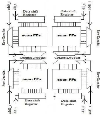
Architecture of SIRAS is shown in Figure 2. Here each SIRAS cluster consists of SFFs configured as SRAM like grid structure. The SFF cell as proposed in [4] is used in our design as shown in Figure 3. ASR is used to shift address bits. When address bits are being shifted-in serially into ASR, data bits are also shifted through Data Shift Register (DSR). Therefore, write operation will be word oriented. Word size is kept nearly equal to size of address bits. This is kept so, because the data and address bits should be shifted simultaneously. For the read operation, the states of the SFFs in the enabled row, chosen by the row decoder are passed to the sense amplifiers using the vertical bidirectional scan data lines.
Figure 2 SERIAL INPUT RAS
The read by the sense amplifiers are passed to multiple input signature register (MISR) which calculates the signature of the test responses.
One SIRAS requires two input test pins for address shift, data in and one output test pin for MISR. Therefore, with the same pin count as conventional RAS, more SIRAS can be accommodated. This allows us to divide SFFs into clusters (multiple SIRAS). Such clustering of SFFs helps in reducing
routing overhead. Also we can operate all clusters in parallel, which reduces test application time. As shown in Figure 2 data bits and address bits are shifted in using ASR and DSR. After all bits are shifted in, DSR contents are written into word enabled by address in ASR. For a given test vector we may not need to write all the SFFs grouped in a word.
Figure 3 SCAN FLIP FLOP CELL [4]
Definition: The bits of a word which need to be written in new test vector are called useful bits.
To minimize test application time, we need to maximize average useful bits per word. We have also proposed algorithm to maximize average useful bits per word.
Example 1: Let’s consider a circuit with 4096 SFFs as shown in Figure 2. Conventional RAS requires 12 address lines to address individual SFFs. In SIRAS three pins (address shift, data in, data out) are required for each cluster. Hence, we can have four SIRAS with same pin count as conventional RAS. Since we have four SIRAS, each SIRAS will have 1024 flip-flops. All four SIRAS can be operated in parallel. As number of address bits and word size should be nearly equal, we will take word size as eight bits. Therefore number of address bits will be seven (total 128 words). Hence, after every 8th clock cycle new value of word and address will be shifted in. And in 9th test clock cycle we can write a word. At the end of 9th test clock cycle 4 words will be written (i.e., 32 bits in 9 clock cycle). Even if on an average half of bits are useful bits, then after 9 test clock cycle we can write 16 useful bits compared to 9 bits for conventional RAS.
3.1 Number of clusters and word Size
For a circuit with N SFFs, conventional RAS needs log N2
⎡ ⎤
⎢ ⎥ address bits as inputs. With the same pin count as conventional RAS, (no. of SIRAS) m ⎢⎣
(
lo g N2)
/ 3⎥⎦can be accommodated, because each SIRAS requires only threepins. Therefore, SFFs per SIRAS will be k =⎡⎢N / m⎤⎥. It is desired to have word size (w) = No. of address bits. Where no. of address bits required is given by⎡⎢log k2 ⎤⎥ .
3.2 Scan flip-flop grouping in SIRAS.
In order to reduce test application time we need to maximize average useful bits per word. This can be achieved by arranging simultaneously changing SFFs in the same word to increase useful bits per word.
We introduce the following the symbols.
‘1’:-Indicates that the present state of the flip-flop is 1 and it need not change for the next test vector.
‘0’:- Indicates that the present state of the flip-flop is 0 and it need not change for the next test vector.
‘D’:- Indicates that the present state of the flip-flop is 1 and it needs to be changed to 0 for the next test vector
‘DN’:-Indicates that the present state of the flip-flop is 0 and it needs to be changed to 1 for the next test vector.
Only those SFFs which assume different logic states in last response vector and next test vector need to be written (i.e. SFFs having D and DN state). All the SFFs having D or DN states simultaneously should be part of the same word to increase useful bits per word. In order to find which SFFs should be part of the same word, a graph is constructed whose nodes are SFFs and edge weights indicating how often both SFFs are written simultaneously. Weight matrix is given in Table 1. If two SFFs need to be written during the same test vector then, the edge between these two SFFs will have minimum weights.
Table 1 Weight Matrix
0 1 D DN
0 1 1 2 2
1 1 1 2 2
D 2 2 0 0
DN 2 2 0 0
Here the weights in the weight matrix are chosen on the basis of the following strategy.
1. {D, 0}, {D, 1}, {DN, 0}, {DN, 1} pairs are given highest weight since those are the SFFs which we don’t want to group together.
2. {D, DN} pairs are given the lowest weights since those are the flops which we would want to group together 3. {0, 1} pairs are given medium weights so that the {0, 1} pairs can group among themselves but they should be prevented from mixing with the {D, DN} pairs.
Note that the numbers given here for weights are not absolute, instead they are only relative keeping in mind the above strategy.
Example 2: Consider two matrices as given below where each row corresponds to a test vector (TV matrix) or the value of the SFFs after the applying the test (Response Vector matrix). Here F1, F2, F3, F4 are SFFs.
Test vector (TV) Response Vector (RV) F1 F2 F3 F4 F1 F2 F3 F4 V1 1 0 1 0 R1 1 1 0 0 V2 1 0 0 1 R2 0 0 1 0 V3 1 0 0 0 R3 0 0 0 1 V4 0 1 0 0 R4 1 1 0 1
Assuming all SFFs to be reset initially, we can make a new transition matrix (TM) with new symbols from the test vector and response vector matrices as show below.
F1 F2 F3 F4 V1 DN 0 DN 0 V2 1 D 0 DN V3 DN 0 D 0 V4 0 DN 0 D
Below, we calculate weights for SFFs F2 and F4. V1 V2 V3 V4
F2 0 D 0 DN F4 0 DN 0 D
W24 1 0 1 0 total = 1+0+1+0=2
Weight of the edge between nodes F2 and F4 is 2. Similarly weights of all edges are calculated. The nodes with lesser weights should be part of the same word. For this example Edge matrix can be given as below.
F1 F2 F3 F4 F1 10000 8 2 8 F2 8 10000 8 2 F3 2 8 10000 8 F4 8 2 8 10000
Assuming a word here as 2 bits, as per matrix {F1, F3} and {F2, F4} shall be part of a word. This arrangement will require total 4 word writes, since {F1, F3} needs to be written for test vectors v1 and v3 and {F2, F4} pair needs to be written for test vectors v2 and v3.This means that we need to write only four words considering all the four test vectors. On the other hand if we would have grouped {F1, F2} and {F3, F4} in a word then it would have require 8 word writes. Here, self loops (i.e. edge form node to itself) are being assigned with very large weight. The problem reduces to a standard travelling salesman problem (TSP). The objective is to find out minimum weight Hamiltonian path in the constructed digraph. We have used approximate method to solve TSP. Any kind of TSP solver could be used for this purpose.
3.3 Approximate Write Test Data Volume Analysis In this section we derive an approximate estimation for write test data volume for SIRAS. To write a word the total
amount of data bits required will be sum of word length and address length. As mentioned earlier these two quantities are equal. If all the bits in a given word are useful the data-bits per SFF (DPF) are 2 bits/SFF. Since all the bits in a given word are not useful the average data-bits per SFF (ADPF) is given by
/η Avg (1) Here, ηAvg is useful bits per word divided by word length. Let dibe the number of SFFs that needs to be written during ith test vector and PI be total number of primary inputs, while applying ith test vector. Hence the estimated test data volume (TDV) required for application of all the test vectors is given by
∑ (2) Where T is the total number of test vectors applied. For the case of conventional RAS, test data volume (TDVCR) can be given as
log ∑
Where, M is the total number of SFFs.
4. VARIABLE WORD LENGTH RANDOM ACCESS SCAN (VWLRAS)
In this section we propose a new architecture for RAS where in multiple columns are enabled to write into multiple SFFs of a row. Similar to the previous architecture the SFFs are arranged as a rectangular array in similar to SRAM like grid architecture. The architecture of the SFF cell is given in the Figure 3. As shown in the Figure 4, we define the following
1. RA - Row decoder address input 2. CA - Column decoder address input
3. NL - Number of columns to be enabled starting from CA
FIGURE -4 VARIABLE WORD LENGTH RAS
Row decoder is same as conventional RAS but column decoder has one more input “NL”. “RA” and “CA” decide starting address of the enabled SFFs in particular row. “NL” decides how many SFFs should be enabled starting from SFF selected by “RA” and “CA”. Let’s consider “RA” is 3,
“CA” is 2 and “NL” is 4. Therefore, in the third row 2nd, 3rd, 4th, 5th and 6th SFFs are enabled for write operation as shown in Figure 4. These entire SFFs will be written with similar logic value either 1 or 0. If “NL” input is zero, then only one column line will be selected.
In this scheme effectively multiple SFFs can be written in one test cycle compared to only one bit in conventional RAS with only one data bit information. The test response read is performed similarly as mentioned in the previous architecture. On an average how many SFFs are being written in one test clock cycle depends on how good SFFs are arranged. Algorithm for arrangement of SFFs which results into reduction in test application time is given below. Here we will use the same symbols as used in Section 3.2. Only weight matrix needs to be changed. In this architecture all those SFFs which are transiting to same state need to be grouped together. Weight matrix for such optimization is given in Table 2.
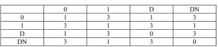
Table 2 Weight Matrix for VWLRAS
0 1 D DN
0 1 3 1 3
1 3 1 3 1
D 1 3 0 3
DN 3 1 3 0
Weight calculation can be carried out in similar manner as described in Section 3.2. It reduces to standard travelling salesman problem (TSP). Any good TSP solver can be used to find optimal arrangement of the SFFs. For choosing the weights we follow the strategy as given below.
1. {D, D}, {DN, DN} are most desired grouping since both SFF required to be written and transit to same state hence we give the least weight.
2. {D, 0}, {0, D}, {DN, 1}, {1, DN} pairs could also be allowed since both SFF end up in same state, but it is given relatively higher weights because this pair is to be chosen only if the first type of grouping is not possible.
3. {0, 0}, {1, 1} pairs could be allowed to group, but still we give higher weight compared to first type which otherwise would prevent the second type of grouping.
4. Remaining pairs are given the highest weights since we need to prevent these pairs from grouping together.
4.1 Approximate Write Test Data volume analysis Every write cycle requires log bits for starting address, log bits to specify the number of lines to be enabled and 1 data bit. There the estimation for write test data volume (TDV) is as given below
TDV log M log n ∑
Where,
TDV = Test data volume M = Total number of SFFs
n = Maximum number of columns that are allowed to be written simultaneously
wi = number of write cycles for ith test vector.
T = number of test vectors
PI = number of primary inputs.
5. EXPERIMENTAL RESULTS
We have computed test vector application time for various ITC 2002, ITC 99 and ISCAS 89 benchmark circuits. While comparing different architectures, we have maintained same pin count for all of them to have fair comparisons. Fully specified test vectors generated by TetraMax ATPG tool from Synopsys, were used for test application time computations. For bit grouping we formulated TSP and solved it using simulated annealing technique.
Table 3 shows the results of test write time for various techniques. We compared our two techniques with conventional RAS [9]. Conventional RAS has parallel address lines and one bit data which are known to be the best in test time. On an average, speed up in (test write time) for smaller circuits is about 2X for SIRAS and about 3X for VWLRAS compared to conventional RAS. As the number of SFFs increases, speed up in test write time compared to conventional RAS also increases. This is evident from the results of d695 (ITC 2002 benchmark circuit having 6384 SFFs) where, speed up of 6.4 and 9.7 in test write time is achieved for SIRAS and VWLRAS respectively. Since test write time is a major part of test application time [4], speed up in test write time will result into significant speed up in test application time as well.
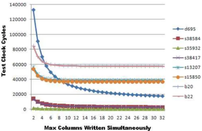
This work uses fully specified test vectors. We have not applied don’t care identification on fully specified test vectors. We will also report the results with partially specified test vectors in the final version if it is accepted. We also studied the maximum number of bits which can be written in single test clock cycle (depends on width of
“NL” input as shown in Figure 5) for VWLRAS. We found that increase in maximum number of bits which can be written in single test clock cycle, results into reduction in test write time initially. However beyond a certain number, further increase in maximum number of bits which can be written in single test clock cycle does not result into significant reduction in test write time. This indicates that for most of the instances, number of columns needed to be enabled together is less then certain number. Based on this observation, we can find the maximum number of bits which can be written in one test clock cycle. Since maximum number of bits which can be written in one test clock cycle has implication on the width of “NL” input (refer Figure 5). Unnecessary increase in maximum number of bits which can be written in single test clock cycle results into increase in routing overhead, test pins required and increase in test data volume. Figure 6 shows the graph between the test write time and maximum number of bits which can be written in a test clock cycle. It is evident from the graph that for all benchmark circuits, reduction in test write time is marginal beyond certain maximum number of bits which can be written in single test clock cycle. We estimated the area
overhead for the proposed new type of address decoder using DesignCompiler by Synopsys to be 50% compared to normal decoders. However decoder is small part of entire chip, therefore the net increase in the area of the whole chip will be very small.
Table 3 Comparison of Test Write Time
Circuit No. Of SFF
Write Time (clock cycles) RAS SIRAS Speed
Up
VWLRAS Speed Up D695 6384 171047 26400 6.47 17591 9.72 S13207 669 100682 50480 1.99 42913 2.34 S15850 597 115825 28052 4.12 37154 3.11 S38584 1452 26638 12700 2.09 7969 3.3
S35932 1728 2377 1030 2.3 763 3.11
S38417 1636 19985 10375 1.92 7212 2.77 B20 490 92557 54852 1.68 58904 1.57 B22 735 90777 54044 1.67 58159 1.56
We observed that VWLRAS is faster than SIRAS. However in this test time computations, we have not taken reading the responses into consideration. SIRAS requires only three test pins. Therefore, we can divide total SFFs into multiple SIRAS. Hence, SIRAS will have less routing overhead compared to VWLRAS.
Figure 6:- Graph of test write time time Vs. Maximum no .of bits which can be written in single test clock cycle.
Table 4 Comparison of write test data volume
circuit Conventional RAS test write data in bits
SIRAS test write
data in bits
Red (%)
VWLRAS test write
data
Red (%)
D695 4572774 2192994 52 1937516 58.6
S13207 1272887 520261 59 476342 62.5
S15850 1186558 460803 61.1 472944 60.1
S38584 755351 253368 66.4 105308 86
S35932 79746 23805 70.1 43749 45.1
S38417 733619 263365 64.1 93855 87.2
B20 933721 454763 51.2 658227 29.5
B22 970511 458206 52.7 685476 29.6
We experimentally calculated write test data volume for standard benchmark circuits. The results shown in Table 4
reveals that write test data volume is significantly less conventional RAS write test data volume for both of our architecture. Also, these results confirm approximate formula given to estimate write test data volumes.
6. CONCLUSION
Random Access Scan is a promising technique which reduces test write time time, test data volume and test power. This paper proposed two effective techniques for test time minimization in the framework of clustered Random Access Scan, SIRAS and VWLRAS. In addition these approaches reduce write test data volume significantly. These techniques exploit the parallelism among the clusters and uses parallel loading of multiple bits. We have also proposed a graph theoretic technique for grouping of the SFFs, which effectively minimizes the test write time time. Experimental results on benchmark circuits show that we can get speedup in the range of 1.5x to 9x, and write test data volume reduction from 30% to 87% compared to conventional Random Access Scan.
The future work in this direction will consider the layout constraints for grouping SFFs. We’ll also consider evaluating exact power figures to evaluate the schemes. We’ll also like evaluate how the architectures proposed by us can be used to speed up the reading of test responses.
7. REFERENCE
[1] H. Ando, “Testing VLSI with RANDOM ACCESS SCAN”, Digest of computer society international conference (COMPCON), 1980, PP. 50-52
[2] D.H. Baik, S. Kajihara, and K.K. Saluja, “Random access scan: A solution to test power, test data volume and test time,” Proceedings of International Conference on VLSI Design, 2004, pp. 883-888.
[3] S. Kajihara, K. Ishida, K. Miyase, “Test Vector Modification for Power Reduction during Scan Testing” Proceedings of VLSI Test Symposium, 2002, pp.160-165.
[4] D.H. Baik and K.K. Saluja, “Progress Random Access Scan: A simultaneous solution to test power, test data volume and test time”, Proceedings of International Test Conference (ITC), 2005, pp. 1-10.
[5] A.S. Mudlapur, V.D. Agrawal, and A.D. Singh, “A Random Scan Architecture to Reduce Hardware Overhead”, Proceedings of International Test Conference (ITC), 2005, pp. 1-9.
[6] C. Yao, K.K.Saluja, and A.A.sinkar, “WOR-BIST: A Complete Test Solution for Designs Meeting Power, Area and Performance Requirements” Proceedings of International Conference on VLSI Design, 2009, pp .479-484.
[7] Yu Hu, Cheng Li, Jia Li, Y-H Han, X-Wei Li, W. Wang, H-W Li,L-T Wang, and X-Q Wen, “Test Data Compression Based on Clustered Random Access Scan”, Proceedings of Asian Test Symposium 2006, pp.231-236.
[8] Y. Hu, X.Fu, X. Fan and H. Fujiwara, “Localized Random Access Scan: Towards Low Area and Routing Overhead”, Proceedings of ASP Design Automation Conference (ASP- DAC) 2008, pp .565-570.
[9] M.L. Bushnell and V.D. Agrawal, Essentials of Electronic Testing for Digital memory and Mixed Signal VLSI Circuits, Springer, 2005.
![Figure 3 SCAN FLIP FLOP CELL [4]](https://thumb-ap.123doks.com/thumbv2/123deta/5752066.26961/3.918.131.415.193.467/figure-scan-flip-flop-cell.webp)