Software-Based Delay Fault Testing of Processor Cores
Virendra Singh
1, 3, Michiko Inoue
1, Kewal K Saluja
2, and Hideo Fujiwara
11
Nara Institute of Science & Technology, Ikoma, Nara 630-0192, Japan
{virend-s, kounoe, fujiwara}@is.aist-nara.ac.jp
2
University of Wisconsin – Madison, U.S.A
3
Central Electronics Engineering Research Institute, Pilani, India
Abstract
Software-based self-testing is a promising approach for the testing of processor cores which are embedded inside a System-on-a-Chip (SoC), as it can apply test vectors in functional mode using its instruction set. This paper presents a software-based self-testing methodology for delay fault testing. Delay faults will affect the circuit functionality only when it can be activated in functional mode. A systematic approach for the generation of test vectors, which are applicable in functional mode, is presented. A graph theoretic model (represented by IE-Graph) is developed in order to model the datapath. A finite state machine model is used for the controller. These models are used for constraint extraction under which a test can be applied in functional mode. This approach uses instruction set architecture, RT level description along with gate level netlist for test generation.
Key words: software-based self-testing, delay fault testing, processor testing, at-speed testing.
1. Introduction
Aggressive processor design methods using giga-hertz clock and deep sub-micron technology are necessitating the use of at speed testing of these processors. It is no longer sufficient to target stuck-at faults, other faults, such as delay faults, are becoming increasingly important to test. At speed testing using external tester is not an economically viable scheme. Self- test is an alternative solution. Widely used self-testing technique, Built In Self Test (BIST), is a structural testing methodology. BIST gives good quality test but requires additional hardware and hence it has area and performance overhead. Further, this may be unacceptable when we want to test an optimized processor core, which is embedded deep inside a System-on-a-Chip (SoC). Once a core is embedded then it is also difficult to access the core for test application. Also, to use BIST, the circuit must also be BIST ready beforehand, which often requires design changes.
Structural BIST operates in orthogonal test mode with pseudorandom test data, which may lead to excessive power dissipation. For at speed testing complex issues related to timing, like multiple clock domain and clock skew, must be resolved. In order to solve these problems, software-based self-testing technique is an alternative. Software based self- testing (functional self testing) methodology uses processor instructions and its functionality in order to test the processor core. Therefore, it has following advantages over structural BIST: 1) it operates in normal mode of operation, 2) There is no area and performance overhead, 3) at speed testing is possible, and 4) no excessive power consumption takes place during test.
Functional self-test can easily be applied on a processor core, embedded deep inside an SoC. This paper focuses on functional self-testing of processor core. We propose a delay fault testing methodology using functional self-test. We treat controller and datapath differently as both have different characteristics. Controller provides constraints on application of test vectors on itself and on the datapath. We first extract the constraints on datapath and controller and use these constraints in the test vector generation process. As the vectors are generated under constraints, instruction(s) to apply the test vectors can always be found.
The paper is organized as follows. Section 2 describes previous work in software based self-testing and section 3 describes the overview of our work and definitions used. Sections 4 and 5 describe testing methodology of datapath and controller respectively. Section 6 discusses test instruction sequence generation and finally the paper concludes with section 7.
IEEE the 12th Asian Test Symposium (ATS'03), pp.68-71, Nov. 2003.
2. Previous work
In a landmark paper in the early 80’s Thatte and Abraham [1] proposed a graph theoretic model for testing a microprocessor, and based on this and functional fault model they developed test procedures to test a microprocessor. Saluja et. al [2] used timing and control information along with processor model [1] to reduce the test complexity. Brahme and Abraham [3] proposed an improved functional model to further reduce the test size. All these approaches use functional fault model but, little if any, fault grading was done on structural model in these approaches.
A number of software based self-test approaches [4,5,6,7,8,9], targeting stuck-at faults, have also been proposed. Shen and Abraham [4] proposed an approach based on instruction randomization. This approach generates a sequence of instructions that enumerates all combinations of operations and systematically selected operands. Batcher and Papachristou [5] also proposed an instruction randomization approach which combines the execution of microprocessor instructions with a small amount of on-chip hardware for randomization of instructions. Both these approaches [4,5] give low fault coverage due to high level of abstraction and they generate large code sequence resulting in large test application time. Chen and Dey [6] used the concept of self-test signature in which they generate structural tests in the form of self- test signatures for functional modules by taking constraints into consideration. These self-test signatures are expanded into test sets using software LFSR during self-test and applied using a test application program. Responses are collected and compared with a response signature stored in memory. Due to pseudorandom nature of this methodology self-test code size and test application time are large. Moreover, efficiency of pseudorandom software based methodology depends on internal architecture and bit width. Paschalis et. al. [7] use self-test routines for functional modules based on deterministic test sets for testing datapath of a processor. Similarly, Krantis et. al. [8,9] proposed a methodology based on instruction set architecture and RT level description while using deterministic test sets to tests every functional component of the processor for all the operations performed by that component. Deterministic nature of these [7,8,9] approaches lead to reduced test code size but these methods find difficult to achieve high fault coverage for complex architectures. Approaches [6,7,8,9] do not explicitly consider the controller.
A software based self-test approach targeting delay faults was proposed by Lai et. al [10,11,12]. This approach, first classifies a path to be functionally testable or untestable. The authors argue that delay defects on the functionally untestable paths will not cause any chip failure. They also suggest that gross delay defects should be tested by transition fault testing. In their method datapath and controller are considered separately. Path classification is performed by extracting a set of constraints for the datapath logic and the controller. In constraint extraction procedure for datapath, all instruction pairs are enumerated and for each instruction pair all possible vector pairs that can be applied to the datapath are derived symbolically. These symbolic vector pairs represent the constraints for datapath testing. This requires a substantial effort to analyze all the instructions and all possible pairs of instructions even though it is not necessary to analyze all the pairs as shown in this paper. For controller, constraints in terms of legitimate bit patterns in registers and correlation between control signals and transition in registers are extracted. A procedure given in [15] is used to classify paths in controller which uses multiple time frames. This procedure uses sequential path classification methodology i.e., in order to classify a path it propagate the transition forward till PO and backward till PI in multiple time frames under the constraints. This is needed because it is not extracting the constraints provided by the state transitions. After classification of paths, constrained ATPG is used to generate the test patterns for testable paths. Lai and Cheng [13] proposed an approach for delay fault testing of a System-on-a-Chip using its own embedded processor instructions, and also proposed a methodology to include new test instructions for testability enhancement and test program size reduction.
3. Overview and definitions
The objective of this work is to develop a procedure for delay fault testing of a processor core that can be used to generate tests for the functional mode of operation of a processor using its instruction set. We use the path delay fault model [20] in this work.
Our methodology considers datapath and controller separately as both of these have different design characteristics. Datapath normally consists of combinational logic blocks and a set of registers, whereas the controller is often described and implemented as a finite state machine. The activities in the datapath are controlled by the controller, thus the function of the datapath and inputs to the datapah are constrained by the controller. Hence, only a subset of structurally applicable test vectors may be applied in functional mode of operation due to the presence of constraints. Similarly, the controller is also constrained by state transitions and signals from the datapath, thus restricting the tests that can be applied to the controller during functional mode of a processor.
We model datapath by an Instruction Execution Graph (IE-Graph) that can be constructed from the instruction set architecture and RT level description of the processor. In our formulation of the test problem IE-Graph is used to extract constraints imposed on the datapath. First, constraints on the control signals that can be applied on the paths between a
pair of registers in consecutive cycles are extracted. Next, constraint on justifiable data inputs (registers) are extracted. Following these, a combinational constrained ATPG is used to generate test vectors under the extracted constraints. Thus, in this approach only those vectors are generated that can be applied functionally. Further, the search space is significantly small as only those states are used during test generation which can cause data transfer to take place on a path between a pair of registers.
For testing the controller the constraints are extracted in the form of state transitions from its RT level description. These constraints also include the values of status signals in the status register and instruction code in the instruction register of the processor. After extracting the constraints, test generation is performed in two-phases. The first phase is the preprocessing stage during which all paths are classified as functionally untestable or potentially functionally testable. The second phase is the combinational constrained ATPG phase during which tests are generated for the paths classified as potentially functionally testable during the first phase. As the vectors must be generated with constraints on the states and inputs to the controller (contents of the instruction register and status register), the number of timeframes that are required for sequential test generation are reduced. In the final phase test instructions are generated using the knowledge of the control signals and contents of the instruction register. Justification and observation instruction sequence generation processes are based on heuristics which minimize the number of instructions and/or the test application time.
Throughout this paper the following concepts and notation will be used.
Definition 1: A path [20] is defined as an ordered set of gates {g0, g1, …, gn}, where g0 is a primary input or output from a FF, and gn is a primary output or input to a FF. Output of a gate gi is an input to gate gi+1 (0<i<n-1).
Definition 2: A path is (enhanced-scan or standard-scan) structurally testable [10] if there exists a structural test for the path, which can be applied through the (enhanced or standard) full-scan chain.
Definition 3: A path is functionally testable [10] if there exists a functional test for that path, otherwise the path is functionally untestable.
A functional two-pattern test does not exist to test a path implies that there does not exist an instruction or an instruction sequence to apply the required test in functional mode of operation. Clearly, functionally untestable paths are never activated in normal (functional) operational mode and we need not target these paths in our approach. We use the following notation to represent signal values.
c: represents a value that does not change in two consecutive timeframes, i.e, it represents a stable 0 or a stable 1 value in two time frames.
x: represents a bit that can be assigned either a logic 0 or a logic 1 value at will.
d: represents bit which is not cared by state transition. It is the same as x, except that legitimate bit pattern in the register has to be justified.
R: represents rising transition. F: represents falling transition.
A constraint can be represented by a vector pair, say P, and the elements of P can be 0, 1, x, c, or d.
Definition 4: A Constraint P is said to cover a constraint Q if P = Q or Q can be obtained from P by assigning 0 and 1 values to x’s in P.
4. Datapath
In this section, we consider paths relevant to data transfer between registers in the datapath. The other paths are treated in the next section. The paths, which are going through the logic in the controller, are considered in the next section, even if they start from and end at some registers in the datapath.
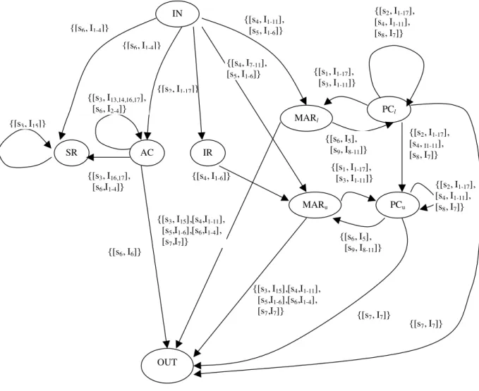
Datapath is modeled by an IE-Graph. This is based on the concept of S-Graph proposed in [1, 3]. However, unlike S- Graph, the IE-Graph contains information about data transfer activities associated with an instruction as well as the state during which a given action takes place. IE-Graph is constructed from the instruction set architecture and register transfer level description and includes architecture registers of the datapath.
Nodes of the IE-Graph are (i) registers, (ii) two special nodes, IN and OUT, which model external world such as memory and I/O devices, (iii) part of registers which can be independently readable and writable, and (iv) equivalent registers (set of registers which behave in the same way with instruction set, as defined by [3]), such as registers in a register file. A directed edge between two nodes is drawn iff there exists at least one instruction which is responsible to transfer data
(with or without manipulation) over the paths between two nodes (registers). Each edge is marked with a set of [state, instruction(s)] pairs, which are responsible for the data transfer between the pair of nodes.
Next we describe a method of construction of IE-Graph using Parwan Processor [17] as an example. Parwan Processor is an accumulator based 8-bit processor with 12-bit address bus. It has 17 instructions, listed in Table 1, and it supports both direct and indirect addressing modes.
Table 1. Instruction set of Parwan processor 1. LDA 6. STA 11. BRA_N 16. ASL
2. AND 7. JSR 12. NOP 17. ASR
3. ADD 8. BRA_V 13. CLA 4. SUB 9. BRA_C 14. CMA 5. JMP 10. BRA_Z 15. CMC
The complete IE-Graph of the Parwan processor is shown in Figure 1.
{[s2, I1-17], [s4, I1-11], [s8, I7]}
Figure1. IE-Graph of Parwan processor
{[s2, I1-17], [s4, I1-11], [s8, I7]}
{[s7, I7]} {[s3, I15],[s4,I1-11],
[s5,I1-6],[s6,I1-4], [s7,I7]}
{[s4, I7-11], [s5, I1-6]}
{[s6, I5], [s9, I8-11]}
{[s2, I1-17], [s4, I1-11], [s8, I7]} {[s1, I1-17],
[s3, I1-11]}
PCu
MARu
{[s3, I16,17], [s6,I1-4]}
{[s6, I1-4]}
{[s2, I1-17]}
{[s4, I1-6]}
{[s1, I1-17], [s3, I1-11]} {[s6, I1-4]}
{[s3, I13,14,16,17], [s6, I2-4]}
{[s4, I1-11], [s5, I1-6]}
{[s6, I5], [s9, I8-11]}
{[s3, I15],[s4,I1-11], [s5,I1-6],[s6,I1-4],
[s7,I7]} {[s6, I6]}
{[s7, I7]} {[s3, I15]}
OUT
PCl
MARl
IR AC
SR
IN
A method of construction of IE-Graph using instruction ASL (Arithmetic shift left – I16) as an example is shown in Figure 2. Execution of this instruction takes 3 states. States s1 and s2 are instruction fetch states and state s3 shifts the contents of AC left by one bit. Fig. 2(a) shows the dataflow between PC and MAR. The registers PC and MAR are split in two registers each as their upper and lower parts can be independently readable and writable. Edges are marked with [s1, I16] as data transfer takes place during state s1 in the execution of instruction I16. Fig. 2(b) shows the data transfers during the next state from MAR to memory (OUT node), memory (IN node) to register IR, and PC to PC for increment. Edges are
marked with [s2, I16]. Fig. 2(c) shows the data transfer from AC to AC and the effect of this transfer on SR; and accordingly the edges are marked as [s3, I16].
(a) [s1, I16] [s1, I16]
MARu
MARl
PCu
PCl [s2, I16] [s2, I16]
[s2, I16] PCl
MARl
PCu
MARu
OUT [s2, I16]
[s2, I16]
[s2, I16]
IR IN
(c) [s3, I16] [s3, I16]
AC SR
(b) Figure 2. Construction of IE-Graph for ASL instruction
Test vector generation process uses instruction set architecture, register transfer level description, and gate level netlist. It is a two-step process. The first step is constraint extraction process and the second step is test vector generation process.
4.1 Constraint extraction
There are two types of constraints imposed on the datapath by the controller. (i) Control constraints, and (ii) Data constraints. Control constraints are the constraints on control signals, which are responsible to transfer data between two registers. These constraints are obtained from IE-Graph and RT level description. Data constraints are the constraints on the justifiable data in the registers under control constraints, which can be obtained using RT level description.
Definition 5: Let there be an edge from node Ri to Ro, marked with [sl, Ip]. The marked state sl is defined as a latching state for the paths represented by that edge.
Data transfer activity from register Ri to Ro takes place in state sl during the execution of instruction Ip and register Ro will be latched. Hence, state sl is defined as a latching state.
Lemma 1: Let <V1, V2> be a test vector pair for a path from register Ri to a register Ro, where test vector V1 is followed by V2 and the edge between these registers is marked with a set of state-instruction pairs {[sl, Ip]}. This vector pair can be a test vector pair in functional mode only if there exists at least one state-instruction pair [sl, Ip] ∈ {[sl, Ip]}, such that (i) vector V2 can be applied in the latching state sl of the instruction Ip, and
(ii) vector V1 can be applied in the state just before the latching state sl of the instruction Ip.
Note that the state just before the latching state include the last states of all the instructions if the latching state is the first state of the instruction marked with it.
During the latching state sl, data transfer (with or without manipulation) from register Ri to Ro takes place and the result is latched in register Ro. Therefore, we can apply the second vector only in the latching state (say sl) and the first vector must be applied in a state just before the latching state (say sj). Two consecutive states sj and sl give the control constraints, and control signals in these states during the execution of instruction(s) marked with the latching state are obtained from RT level description. Constraints on the states during which we can apply the test vectors <V1, V2> take care of justification of the control signals in the functional mode of testing. Data constraints in the form of justifiable data in the input register of the register pair and other registers required for the execution of marked instruction are obtained from RT level description.
Lemma 2: Paths from register Ri to Ro are functionally untestable if the following conditions exist, 1. Ri is not an IN node, and
2. Ri has no incoming edge marked with the state just before the latching state (sl) of the instruction Ip for any [sl,Ip] marked on the edge (Ri, Ro).
If conditions stated in Lemma 2 exist then transition cannot be launched from register Ri. Hence, the paths between a register pair Ri and Ro are functionally untestable. Otherwise, these paths are classified as potentially functionally testable paths (PFTP). We need to extract the data constraints for the potentially functionally testable paths. Covering relation, defined in section 3, helps reduce the number of constraints.
Example 1. Constraints on paths between AC and AC in Parwan processor
The edge between nodes AC and AC is marked with {[s3, (I13-14, I16-17)], [s6, I2-4]}, as shown in Figure 1. AC is neither an IN node nor it has any incoming edge which is marked with just previous state of its latching state s3 or s6. Therefore, using Lemma 2 we can conclude that paths from AC to AC are functionally untestable.
Example 2: Paths from IN to AC
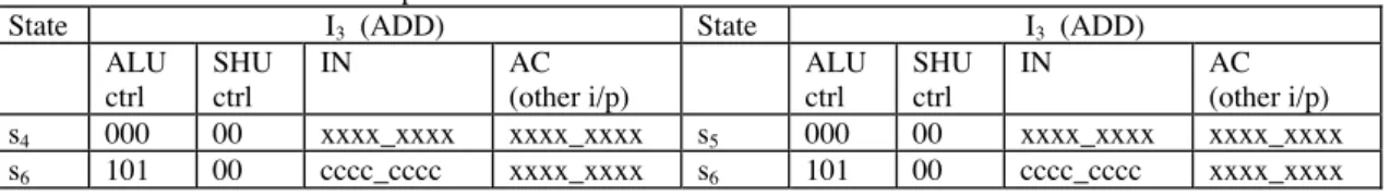
The edge between nodes IN and AC is marked with [s6, I1-4], as shown in Figure 1. These paths are PFTP in accordance with Lemma 2, as input node is an IN node, and the latching state for these paths is s6. Therefore, control constraints are the control signals generated in state s4 or s5 followed by s6 for the instructions I1, I2, I3 or I4. This is obtained from IE- Graph and RT level description. Data constraints can be obtained in the state s4 followed by state s6 or state s5 followed by s6, for the instructions I1, I2, I3 and I4. Data constraints for the instruction I3 are shown in Table 2. Here we assume that when input to a combinational logic is in high impedance state then it can hold the logic value that is applied before the high impedance state. Parwan processor uses tristate buses. These trisate buses are responsible for the constraints on IN node.
Table 2. Data constraints for the paths between IN and AC
State I3 (ADD) State I3 (ADD)
ALU ctrl
SHU ctrl
IN AC
(other i/p)
ALU ctrl
SHU ctrl
IN AC
(other i/p)
s4 000 00 xxxx_xxxx xxxx_xxxx s5 000 00 xxxx_xxxx xxxx_xxxx
s6 101 00 cccc_cccc xxxx_xxxx s6 101 00 cccc_cccc xxxx_xxxx
For instruction I3, both control constraints, s4 followed by s6 and s5 followed by s6, are identical. Hence, using the covering relation one of these two constraints can be eliminated. All other constraints are extracted similarly.
4.2 Test vector generation procedure
Constrained ATPG is used to generate the test vectors for the potentially functionally testable paths under the extracted constraints. Path lists between a register pair and their corresponding constraints are provided as inputs to an ATPG along with gate level netlist and it returns the test vectors for the testable paths.
Procedures to extract the constraints and test generation is given in Figure 3. This procedure systematically extracts the constraints using IE-Graph and uses constrained ATPG to generate the test vectors.
Constraint Extraction Procedure 1. Constraint path pair set W = Φ
2. for nodes Ri (i = 1 to n) { // there are n nodes in IE-Graph // 3. for each edge (Rj, Rj) (j = 1 to m) { // there are m edges from node Ri // 4. if paths are PFTP then { // (using Lemma 2) //
5. Pij = Set of all paths between Ri and Rj
6. Cij = Set of constraints for the paths from node Ri to node Rj 7. W = W ∪ {[ Cij, Pij ]}
8. } 9. } 10. }
Test Generation Procedure Constrained ATPG process
Input : Constraint path pair set W, Gate level net list Output : Set of testable path with their test vector pairs Figure 3. Constraint extraction and Test generation Procedures
5.
Controller
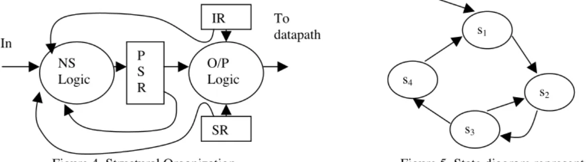
Controller is a sequential circuit that is normally implemented as mealy type or moore type finite state machine
.
Structural organization of the controller and its finite state abstraction model are shown in Figure 4 and Figure 5 respectively. Where PSR is present state register, SR is status register, and IR is instruction register. In this section, we treat all the paths that go through the logic in the controller.s4
s3
s2
s1
Figure 4. Structural Organization Figure 5. State diagram representation IR
P S R
SR NS
Logic
O/P Logic
To datapath In
Controller generates control signals for datapath in order to execute an instruction. It may take several cycles. Test vectors applicable in functional mode of operation to the controller are restricted by the state transitions. If we never find a sequence of valid state transitions which could create a transition and propagate it along a path then that path is a functionally untestable path, even though that may be structurally testable (test vectors can be applied using full scan or enhance scan approach). Therefore, some paths, which are structurally testable, may not be functionally testable. Hence, we extract constraints on state transitions prior to test generation.
5.1 Constraint Extraction
Change of state of controller is determined by the values in registers (IR and SR), inputs and present state. Input from registers IR and SR (i.e., registers other than the present state register (PSR)) are treated as constrained primary input (CPI). Therefore, we need to extract two types of constraints (i) constraints on state transition, and (ii) constraint on legitimate values in IR and SR registers, as these are treated as constrained primary input.
(i) State transition constraints
Constraints on state transition can be extracted by extracting possible valid state transition under legitimate values in IR, SR and input, by using instruction set architecture and RT level description. We show it using Parwan processor as an example. Table 3 shows a part of the state transition table of Parwan processor.
Table 3. State transition table of Parwan processor (partial)
PS NS IR (PS) IR (NS) SR
(PS) SR (NS)
In (PS) {Intrpt.} s1 dddd_dddd cccc_cccc dddd cccc 1 s1
s2 dddd_dddd cccc_cccc dddd cccc 0 0xxx_xxxx dddd cccc d 100x_xxxx dddd cccc d 101x_xxxx dddd cccc d 110x_xxxx dddd cccc d 1110_0000 dddd cccc d 1110_0001 dddd cccc d 1110_0010 dddd cccc d 1110_0100 dddd cccc d 1110_1000 dddd cccc d s2 s3 dddd_dddd
1110_1001 dddd cccc d
This Table shows that when present state is s1 then next state will be either s1 or s2 depending on the value of input, and independent of values in IR and SR registers. During these state transitions (s1 to s1 or s2) register IR and SR can have any legitimate value in the present state (s1) and must have the same values in next state (s1 or s2). Hence, we cannot launch transition from IR and SR during these state transitions. When present state is s2 then next state is always s3. IR can have
any legitimate value in present state (s2) as well as in next state (s3). Therefore, transition can be launched from IR during the state transition s2 to s3. Similarly, we can extract other constraints. A test vector can be represented as (state, CPI, PI). (ii) Constraints on legitimate values in IR and SR register (registers other than the present state register):
A set of legitimate values in the registers other than the present state register can be obtained from its instruction set architecture and RT level description. For example, IR of Parwan processor can have some of the legitimate bit patterns which are specified as {IR, <0xxx_xxxx, 10xx_xxxx, 110x_xxxx, 1111_0100, 1111_0010, 1111_0001, 1110_0000, 1110_0001, 1110_0010, 1110_0100, 1110_1000, 1110_1001>}.
5.2 Test generation process
Test generation process is a two-phase process which uses extracted constraints. The first phase is the preprocessing phase, which classifies paths as potentially functionally testable (PFTP) or functionally untestable (FUTP). Functionally untestable paths are removed from the path list. The second phase generates the test vectors for potentially functionally testable paths if these are functionally testable under the extracted constraints.
Phase 1: Preprocessing
Preprocessing classifies a path as potentially functionally testable or functionally untestable by using state transition diagram and gate level implementation.
There are three types of paths in a controller 1. PSR to PSR
2. Primary input or constraint primary input (registers IR and SR) to present state register (PSR) 3. PI, CPI, or PSR to a register in datapath.
Paths from PSR to PSR are only responsible for sequential behavior of the controller circuit. For preprocessing, we construct a table that shows transition on bits in PSR and other registers with state transitions. Table 4 shows transition on bits in PSR with state transitions for Parwan processor when states are binary encoded.
Table 4. Transition on bits in PSR with state transition (Parwan Processor)
bit s1 s2 s3 s4 s5 s6 s7 s8 s9
R s9
b3
F s1
R s5, s6, s7
b2
F s1, s2 s1
R s3
b1
F s5, s6, s9
R s2 s4 s6 s8
b0
F s3 s5, s7, s9 s1 s1
This table shows that there can be rising transition on bit b3 only when there is a state transition from state s4 to s9. There can be falling transition on b3 only when there is a state transition from state s9 to s1.
Lemma 3: Paths between bit i in register R1 and bit j in register R2 (registers R1 and R2 need not be different) in controller circuit are functionally untestable paths for a transition (rising or falling) if
(i) there does not exist a valid state transition si to sj to launch the transition at bit i, or
(ii) there does not exist a state transition sp to sq which can receive the launched transition or its inverse (receive falling transition when rising is launched) at bit j, such that sj = sp.
A path is functionally testable if we can create a transition and propagate its effect along the path. If the conditions stated in Lemma 3 exist then we either cannot launch a transition or cannot propagate the created transition. Hence, the paths between bit i in register R1 and bit j in register R2 are FUTPs. Otherwise, these paths are classified as PFTP as transition can be created and may be propagated if values in other registers are justifiable. We also get precise constraints under which these paths can be tested using state transition table
1. PSR to PSR path classification (Paths from controller to controller):
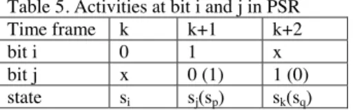
A path between bit i and bit j in PSR can be classified as follows for rising transition, using Lemma 3. We consider 3 consecutive time frames as shown in following table. Activities at bit i and j in PSR and required state transitions are listed in Table 5.
Table 5. Activities at bit i and j in PSR
Time frame k k+1 k+2
bit i 0 1 x
bit j x 0 (1) 1 (0)
state si sj(sp) sk(sq)
These paths are PFTP iff either si to sj to sk, or si to sp to sq state transition sequence exists.
Example 3: PSR to PSR paths classification in Parwan processor when states are binary encoded. Table 3 shows transition on bits in PSR with state transitions. Paths from bit b3 to b3 (for rising transition) are classified as PFTP as state transition sequence s4 to s9 to s1 exists. Similarly, paths from b2 to b1 (for rising transition) are classified as FUTP because no one state transition sequence exists to test these paths, where as paths from b2 to b1 (for falling transition) are classified as a PFTP because a state transition sequence s6 to s2 to s3 exists. State transition sequence s6 to s2 to s3 is an exact constraint for these paths (b2 to b1, falling transition) under which these can be a tested if other values are justifiable. Similarly, we can find out all PFTPs, which are the potential candidates for the next phase.
2. Paths from PI or CPI to bit i in PSR (Paths from input or datapath to controller) classification
(i) Paths from PI to bit i in PSR are classified as PFTP, iff there exists a state sequence (si to sj), which can receive a transition at bit i.
(ii) Paths from CPI to bit i in PSR are classified as PFTP, iff there exist a valid state transition (si to sj) to create a transition at CPI (register IR or SR) and there exists a valid state transition (sj to sp) at bit i of PSR (according to Lemma 2)
3. Paths from CPI or PSR to a register in datapath (Paths from controller to datapath) are classified as PFTP, iff (i) there exists a state sequence (si to sj) which can launch a transition at bit i in PSR or CPI, and
(ii) the register in the datapath, where these paths terminate, has an incoming edge, marked with state sj in IE-Graph and state si and sj are two consecutive states of the marked instruction Ip.
Phase 2: Test generation
A constrained combinational ATPG is used to generate the test vectors for the paths, which are, classified as potentially functionally testable paths under the extracted constraints. ATPG is given with a set of PFTP along with their respective constraints. ATPG will return the test vectors if a path is testable under constraints.
This approach extracts the constraints in the form of state transitions and classifies the paths as functionally untestable or potentially functionally testable. Functionally untestable paths are removed from the path list. It uses combinational constraint ATPG to generate test vectors. Therefore, we need not to consider multiple time frames for all the paths like a sequential ATPG, as sequential behavior is taken care by the state transition in our approach, which in turn reduces the complexity of test generation.
6. Test instruction sequence generation
The generated test vector pairs are assigned to control signals and registers. Control signals and value(s) in IR in two consecutive time frames give the test instruction(s). Data in registers and in memory, which will be used by the test instruction, must be justified, using justification instruction. The result from the output register must be transferred to memory using observation instructions. For example, vector pairs are (V1 = {ALU ctrl=000, SHU ctrl=00, AC=48H, IN=24H}, V2 = {ALU ctrl=111, SHU ctrl=00, AC=48H, IN=04}). This shows that the test instruction will be SUB instruction and the value at x24H must be 04H. Value in AC must be 48H which can be justified by using LDA mem[1], and the result from AC is transferred using STA mem[2]. So, we need three instructions LDA mem[1], SUB mem[3], and STA mem[2].
Some heuristics can be used for instruction justification process in order to reduce the test program size or test application time.
7. Conclusion
This paper, presented a systematic approach for delay fault testing using processor instruction set. A graph theoretic model for datapath is developed to model the activities in the datapath. We can efficiently extract the constraints for paths between register pairs using this model. Controller is modeled as a finite state machine and constraints on state transitions are extracted. This will eliminate the need of multiple time frame consideration for test generation, as we extract the constraints on state transitions, and reduces the test generation complexity. Constrained combinational ATPG is used for test generation.
Experiments on benchmark microprocessors are yet to be carried out. Some efficient heuristics for the generation of justification instruction, which can minimize the test size or test application time, are yet to be considered.
Acknowledgement
This work was supported in part by Semiconductor Technology Academic Research Center (STARC) under the research project.
References
[1]. S.M. Thatte and J.A. Abraham, “Test generation for microprocessors”, IEEE Trans. on Computers, Vol. C-29, No.6, June 1980, pp. 429-441.
[2]. Kewal K Saluja, Li Shen, and S.Y.H. Su, “A simplified Algorithm for Testing Microprocessors”, in Proc. of the International Test Conference, 1983, pp.668-675.
[3] . D. Brahme and J.A. Abraham, “Functional Testing of Microprocessors”, IEEE Trans. on Computers, vol. 33, No. 6, June 1984, pp. 475-484.
[4]. J. Shen and J.A. Abraham, “Native Mode Functional Test Generation for Processors with Applications to Self Test and Design Validation”, in Proc. of the International Test Conference 1998, pp. 990-999.
[5]. K. Batcher and C. Papachristou, “Instruction Randomization Self Test for Processor Cores” in Proc. of the VLSI Test Symposium 1999, p. 34-40.
[6]. Li Chen, and Sujit Dey, “Software-Based Self-Testing Methodology for Processor Cores”, IEEE Trans. on CAD of Integrated Circuits and Systems, Vol. 20, No.3, March 2001, pp. 369-380.
[7]. A. Paschalis, D. Gizopoulos, N. Krantis, M. Psarakis, and Y. Zorian, “Deterministic Software-Based Self-Testing of Embedded Processor Cores”, Design Automation & Test in Europe 2001, Munich, Germany, March 2001.
[8]. N. Krantis, D. Gizopoulos, A. Paschalis, and Y. Zorian, “Instruction-Based Self-Testing of Processor Cores”, in Proc. of the VLSI Test Symposium 2002.
[9]. N. Krantis, A. Paschalis, D. Gizopoulos, and Y. Zorian, “Instruction-Based Self-Testing of Processor Cores”, Journal of Electronic Testing: Theory and Application (JETTA) 19, 2003, pp 103-112.
[10]. W.-C. Lai, A. Krstic, and K.-T. Cheng, “On Testing the Path Delay Faults of a Microprocessor Using its Instruction Set”, Proc. of the VLSI Test Symposium 2000, pp. 15-20.
[11]. W.-C. Lai, A. Krstic, and K.-T. Cheng, “Test Program Synthesis for Path Delay Faults in Microprocessor Cores”, in Proc. of International Test Conference 2000.
[12]. W.-C. Lai, A.Krstic, and K.-T. Cheng, “Functionally Testable Path Delay Faults on a Microprocessor”, IEEE Design & Test of Computers, Oct-Dec 2000, pp 6-14.
[13] W.-C. Lai, and K.-T. Cheng, “Instruction-Level DFT for Testing Processor and IP Cores in System-on-a-Chip”, Proc. of the Design Automation Conference (DAC 01), ACM Press, NY, 2001, pp. 59-64.
[14]. A. Krstic, Li Chen, W.-C. Lai, K.-T. Cheng, and Sujit Dey, “ Embedded Software-Based Self-Test for Programmable Core-Based Designs”, IEEE Design & Test of Computers, July-August 2002, pp. 18-27.
[15]. A. Krstic, S.T. Chakradhar, and K.-T. Cheng, “Testable Path Delay Fault Cover for Sequential Circuts”, Journal of Information Science and Engineering 16, 2000, pp. 673-686.
[16]. K.-T. Cheng, and H.-C. Chen, “Classification and Identification of Nonrobust Untestable Path Delay Faults” IEEE Trans. On CAD of Integrated Circuits and Systems, Vol.15, No.8, Aug. 1996, pp.845-853.
[17]. Z. Navabi, VHDL: Analysis and Modeling of Digital Systems, McGraw-Hill, New York, 1997.
[18]. J.L. Hennessy and D.A. Patterson, Computer Architecture: A Quantitative Approach, Morgan Kaufmann, 1996. [19]. M.Gumm, VLSI Design Course: VHDL-Modeling and Synthesis of DLXS RISC Processor, University of Stuttgart,
Germany, Dec. 1995.
[20]. A. Krstic and K.-T. Cheng, Delay fault testing for VLSI circuits, Kluwer Academic Publishers, 1998.