Design for Two-Pattern Testability of Controller-Data Path Circuits
Md. Altaf-Ul-Amin, Satoshi Ohtake and Hideo Fujiwara
Nara Institute of Science and Technology, Ikoma, Nara 630-0101, Japan E-mail: {amin-m, ohtake, fujiwara}@is.aist-nara.ac.jp
Abstract: This paper introduces a design for testability (DFT) scheme for delay faults of a controller-data path circuit. The scheme makes use of both scan and non-scan techniques. Firstly, the data path is transformed into a hierarchically two-pattern testable (HTPT) data path based on a non-scan approach. Then an enhanced scan (ES) chain is inserted on the control lines and the status lines. The ES chain is extended via the state register of the controller. If necessary, the data path is further modified. Then a test controller is designed and integrated to the circuit. Our approach is mostly based on path delay fault model. However the multiplexer (MUX) select lines and register load lines are tested as register transfer level (RTL) segments. For a given circuit, the area overhead incurred by our scheme decreases reasonably with the increase in bit-width of the data path of the circuit. The proposed scheme support hierarchical test generation and can achieve fault coverage similar to that of the ES approach.
1. Introduction
Two-pattern test is necessary to detect delay faults. The importance of delay testing has soared in recent years to keep pace with the rapid increase in speed of integrated circuits. Testing delay faults in sequential circuits is significantly more difficult than testing delay faults in combinational circuits. This is because application of an arbitrary two-pattern test is not possible to non-scan or standard-scan sequential circuits [1]. Functional justification [2] and scan shifting [3] techniques are used to apply two-pattern test in circuits with standard-scan. However, these techniques cannot guarantee the application of arbitrary two-pattern test. The scheme that can apply arbitrary two-pattern test to a sequential circuit is the ES design [4] [5]. ES flip-plops can store two bits and can apply them in consecutive clocks. However the area overhead of the ES approach is very high. Another disadvantage of the ES approach is that the test application time is very long because of scan operation.
A controller-data path circuit is a sequential circuit. A controller is usually a finite state machine. It consists of a state registers and a combinational logic block. Behaviorally a data path is represented by a data flow graph, in which nodes represent operations (addition,
multiplication etc.) and edges represent data variables. Structurally, the data path consists of operational modules, registers, MUXs and buses. The controller applies control signals to the data path in each time step and thus guides the data path in making computations. In some circuits, the controller receives status signal from the data path in some time steps. In [6], we presented a method to transform a data path to an HTPT one. As an extension to that, in this paper we develop a scheme for two-pattern testability of a controller-data path circuit. The
model we
consider in our approach for a controller-data path circuit is shown in Fig.1. In this model, registers separate the controller and the data path. The register on the control lines is referred to as control line register (CLR) and the register on the status lines is referred to as the status line register (SLR). We also assume that the circuit is a synchronous sequential circuit.
The proposed scheme is developed mostly on path delay fault model. However, to make the delay testing consistent with the overall operation of a controller-data path circuit, we resort to segment delay fault model for MUX select lines and register load lines. The scheme makes use of both scan and non-scan techniques. We first transform the data path to an HTPT data path by applying a non-scan DFT method [6]. An ES chain is inserted via the CLR, SLR and the state registers of the controller. If necessary, the data path is further modified to facilitate the testing of the path segments represented by MUX select lines and register load lines. A test controller is then designed and appropriately added to the circuit. For a given circuit, the area overhead incurred by our scheme decreases reasonably with the increase in bit-width of the data path of the circuit. The advantages of the proposed scheme are (i) hierarchical test generation cab be used and (ii) fault coverage can be achieved similar to the ES approach.
Data Path S
L R C L Controller R
State register PO PI
PI
PO
Fig. 1: A controller-data path circuit
IEEE the 11th Asian Test Symposium (ATS'02), pp. 73-79, Nov. 2002.
2. The HTPT Data Path
In this section, we discuss the HTPT data path. We first introduce the concept of RTL paths. In an RTL circuit of a data path, the paths that, (i) start at a primary input (PI) and end at a register or (ii) start at a register and end at another/same (in case of feedback) register or (iii) start at a register and end at a primary output (PO)/SLR or (iv) start at a PI and end at a PO/SLR are the RTL paths. It is obvious that the sequential depth of an RTL path is one.
“PI1-R1” and “R1-ADD-M6-R4” are two examples of RTL paths in the arbitrary and simple data path of Fig. 2.
In the lower hierarchy, each RTL path consists of a number of 1-bit wide paths. These individual 1-bit wide paths may be classified as robust, non-robust, functional sensitizable and functional unsensitizable paths. To guarantee the timing performance, it is necessary to test the robust, non-robust and functional sensitizable (FS) paths [1].
Path delay fault testing requires launching a transition at the starting of a path by applying a pair of vectors, propagating the transition along the path and allowing fault effect observation from the end of the path [1]. However, many of the RTL paths in the data path neither start at a PI nor end at a PO. Therefore, some paths are necessary to ensure the propagation of test data (test vectors and test responses) from PIs to appropriate registers and from appropriate registers to POs. Paths used for the propagation of test vectors is referred to as control paths and paths used for the propagation of test responses is referred to as observation paths. Any logic value can be propagated along the control paths and the observation paths. An RTL path may cross one or more multiplexers
(MUXs) and operational modules. If an input of a MUX or an operational module is on an RTL path then this input is an on-input of the path. Other input/inputs, which are not on the path, are called off-inputs.
MUXs are common elements in a data path and are used as interconnecting units. Let us consider a 2 to 1 MUX as shown in Fig. 3. Both A and B are n-bit wide. C is the control input. If C selects A then, (i) propagation of signals from A(A1,……An) to O(O1,…….On) is robust (off-inputs remain stable at non- controlling value) and independent of the signals at B and (ii) there is no merging gate among the paths (A1 to O1), (A2 to O2),……..(An to On) i.e. there are only n mutually independent (1-bit wide) paths from A to O. The case for the path from B to O is similar. Therefore, while testing any RTL path crossing one or more MUXs the select input/inputs should be such that they select the on-input/inputs of the MUX/MUXs and the off-input/inputs of the MUX/MUXs are don’t care. For example, to test the path "PI2-M1-R2" (Fig. 2), two-pattern vectors should be applied at PI2 and test responses should be captured at R2. The off-input of M1 may be don't care.
Many RTL paths cross not only MUXs but also operational modules. In the following example, we discuss such a path.
Example 1: The path "R1-M3-M5-MULT-R5" in Fig. 2 crosses the operational module MULT. The segment "R1- M3-M5-" of this path is like a wire in a sense that the signal values at R1 appear unchanged at the output of the M5 if the control inputs of the MUXs select the on-inputs. Again the segment "-R5" on the output side of MULT is obviously like a wire. The core segment of this path is the part of the path inside the MULT. In other words the test vector set required to test the part of the path inside the MULT is the same as to test the whole path "R1-M3-M5- MULT-R5". These test vectors can be generated by separately considering the gate level circuit structure of the MULT. Obviously the bit width of these test vectors spans both inputs of the MULT. Suppose, bits of the test vectors to be applied to the off-input of the MULT are not all don't cares. Hence to test the path "R1-M3-M5-MULT- R5", test vectors should be applied not only at R1 but also at the off-input of the MULT. Test vectors can be applied at the off-input of the MULT from register R2. Therefore, we say that the RTL path "R1-M3-M5-MULT-R5" is an HTPT path if, (i) there exist two control paths from primary input/inputs to R1 and R2 that support the application of two-pattern vectors and (ii) there exists an
M1 1 0 R1
R2
R4 R3
R5 ADD
MULT M2 1
0
M3 1 M4 1 0
0
M5 1 0
M6 1 0 One
One m2
l3
m4
m6
l4
m3
m5
l5
l2 m1
l1 PI1
PO1 PO2
PI2
Fig. 2: An arbitrary simple data path
A1
B1
An
Bn
O1
O2
C
Fig. 3: n-bit wide 2 to 1 MUX
observation path to propagate the test responses from R5 to a primary output.
Definition 1: The set of control paths and an observation path that are sufficient to ensure the hierarchical two- pattern testability of an RTL path is referred to as the test plan of the path.
Referring to Fig. 2, the test plan of the RTL path "R1- M3-M5-MULT-R5" consists of disjoint control paths
"PI1-R1" and "PI2-M1-R2" and the observation path “R5- PO2”. It is noticeable that these control and observation paths are also the test plan of the RTL path "R2-MULT- R5". A test plan can alternatively be represented as a sequence of control vectors [7]. The control vector sequence guides the propagation of two-pattern vectors from PIs to appropriate registers and the propagation of the test responses from appropriate register to some PO. The sequence of Table 1 shows the test plan of the path
"R1-M3-M5-MULT-R5" of Fig. 2. Control signals that are not related to this test plan are not shown in this table.
Time PI1 PI2 m1 m3 m5 l1 l2 l5 PO2
1 C C 0 X X 1 1 X -
2 C C 0 1 1 1 1 X -
3 X X X 1 1 X X 1 -
4 X X X X X X X X O
Definition2: A data path is an HTPT data path if each of its RTL paths has a test plan.
We presented a DFT method to transform a data path to an HTPT data path in [6]. Fig. 4 shows the HTPT equivalent of the data path of Fig. 2 transformed by following the method of [6]. The thru function and the test MUX are the added DFT elements. An important property
of an HTPT data path is that there exists at least one control path from some PI to each register and at least one observation path from each register to some PO.
3. RTL Segments and Its Testing
In this paper, we consider MUX select lines and register load lines as RTL segments. Each segment starts at the CLR and ends at a MUX or a register of the data path. A transition at the select line of a MUX ensures non- controlling or controlling values to certain lines internal to the MUX and thus allows the signals of one of the data inputs to propagate to the output. A transition at the load line of a register determines whether the register should load or not load the data from its input in the following clock. We sensitize a transition along an RTL segment only from CLR to respective MUXs or registers. We test delay faults along these segments using an approach that is consistent with the overall operation of a controller-data path circuit. Our approach is developed in the perspective of RTL i.e. in a broader sense we assume the registers and MUXs as primitive elements. The key to our approach is based on the fact that a delay fault along a MUX select line or a register load line is supposed to change the data flow in the data path. In the following discussion we clarify our approach.
Lemma 1: A delay fault along the path segment represented by a MUX select line prevents the propagation of appropriate data from the MUX’s input side to the output side within specified time.
Proof: In Fig. 5, a rising transition is shown at the start of the multiplexer select line. Before transition, B propagates to O and after transition A propagates to O. Therefore any delay along the select line will delay the propagation of signal from A to O.
Corollary 1: The effect of a delay fault along a path segment represented by the select line of a 2-input MUX can be successfully observed at its output if its input values are different.
Proof: Referring to Fig. 5, before transition O=B and after transition O=A. If A=B then the transition has no effect at the output. Hence by observing the output it is not possible to decide whether the select line has a delay fault or not. But, if A!"# $%&# '()# *+',+'# -.# /$,'+0)&# $1')0# nominal propagation delay then it is possible to detect whether the select line has a delay fault or not.
Definition 3: The critical segment of a line in a data path is the longest possible segment of unity sequential depth that starts at the line and ends at a register (in the direction of the data flow) or a PO.
In the following example we explain a typical method of testing delay fault along a multiplexer select line. Table 1: An example of a test plan
C: apply test pattern to PI X: don’t care
O: observe test response at PO -: Need not be observed
M1 1 0 R1
R2
R4 R3
R5 ADD
MULT M2 1
0
M3 1 M4 1 0
0
M5 1 0
M6 1 0 One
One m2
l3
m4
m6
l4
m3
m5
l5
l2 m1
l1 PI1
PO1
PO2 PI2
1 0
thru
Test MUX mt
Fig. 4: The HTPT equivalent of the data path of Fig. 2
Fig 5. A MUX and its select line C
L R
O B A
0 1
Example 2: Referring to Fig. 4, the inputs of M3 are connected to R1 and R4 and m3 is the select line of M3. Let in some clock t0, any two values A and B such that A!" are loaded to R1 and R4, respectively and some known value C is loaded to R2. Also a rising transition is launched at the start of m3 (at CLR) and the path from the output of M3 via M5 to MULT is selected in t0. In t1 (the following clock) the output of the MULT is loaded to R2. For correct data path operation, A*C (bits of lower half) should be loaded to R2. But if a delay fault along m3 exists, B*C (bits of lower half) or some other incorrect value is loaded to R2. Since A!", it is possible to detect the delay fault along m3 (if present) by observing the value that R2 assumes at the clock cycle t1. However, the values of A, B and C should be such that bits of lower half of A*C does not match with those of B*C. Notice that here the test response can also be loaded to R5. However, we choose R2 because R2 is at the end of the critical segment of the output of M3. If the test passes for the case of the critical segment, it will also pass for the other segments. From the perspective of RTL, it is enough that A!" for this method of testing. However, with an insight to the gate-level structure of a MUX, we choose A and B such that every bit of A is different from the corresponding bit of B. This partially relaxes our assumption that a MUX is a primitive element.
Now we explain how to apply the typical method
descried above using the ES chain along the CLR. The ES chain can store and hold two bits for each control signal. Let l1=1, thru=1, mt=0, m6=0, m3=0, m5=X, m1=0, l2=1, l5=X are shifted into the ES chain as the first bits and l1=1, thru=X, mt=X, m6=X, m3=1, m5=1, m1=1, l2=1, l5=1 as the second bits. For other control signals both bits are don’t care. The waveform of Fig. 6 illustrates the events of the typical method descried above for a fault- free case and a typical faulty case. The events are regulated by exercising a “hold-shift-hold” sequence of the ES chain. The rising transition at m3 is launched in the clock t0 using the shift operation. Before transition the first bits and after transition the second bits are held in the CLR for required number of clock cycles. In the clock t1, numerical value 1 is loaded to R1 to ensure a thru function
to MULT. Similar method can be used to test a falling delay fault along a MUX select line.
Definition 4: The general controllability (known controllability) Cg (Ck) of a line in a data path with respect to some clock is the ability of controlling the line in that clock to any desired value (some known value) by appropriately controlling the PIs and by using the hold and shift properties of the ES chain along the CLR.
Definition 5: The observability (verifiability) O (V) of a line in a data path with respect to some clock is the ability to propagate the value (the signature of the value) that the line assumes in that clock to some PO by appropriately controlling the PIs and by using the hold and shift properties of the ES chain along the CLR.
Definition 6: The O (V) of a line in a data path with respect to some clock is called the critical observility (critical verifiability) Oc (Vc) while (i) the process of propagation is performed through the critical segment of the line and (ii) the propagation reaches beyond the critical segment in the immediately following clock. Theorem 1: The (rising/falling) delay fault along the select line of a MUX in a data path is testable if the following requirements are fulfilled with respect to a certain clock.
(i) The ability to launch a (rising/falling) transition at the start of the select line of the MUX.
(ii) Cg of both of the inputs of the MUX, or Cg of an input and Ck of another input.
(iii) Oc / Vc of the output of the MUX.
Proof: Requirement 1 is obviously necessary for delay testing. The delay fault along the select line of a MUX can be detected by applying two different values at the inputs of the MUX (Corollary 1). Requirement 2 allows the application of two values to two inputs of the MUX, which are different from each other at every bit. Requirement 3 allows the observation of the test response in a way that is consistent for delay testing.
Lemma 2: The rising delay fault along the path segment represented by the load line of a register prevents it from loading data in the following clock (assuming that logic 1 enables the register).
Proof: The proof of this lemma is obvious.
In the following example we explain a typical method of testing rising delay fault along a register load line. Example 3: In Fig. 4, l3 is the load line of R3. Suppose initially l3 is at logic 0 i.e. R3 is disabled. Let, in the clock t0, some known value A is loaded to R1, the path from R1 to R3 is selected (using the thru to ADD) and a rising transition is launched at the start of l3. For correct data path operation, A should be loaded to R3 in the following clock t1. But if there is a delay fault along l3, R3 fails to load A in t1. So, observing the value that R3 contains in the clock t1 can test the fault. Since R3 is initially disabled the value it contains before loading A is unknown. Let this unknown value is U. Hence the test is invalid, if somehow A completely matches with U. If A is arbitrarily chosen
B A 1 X
C
X X
X B A 1 X
X B X
C A*C
X X
A*C X
PI1 PI2 R1 R4 R2 R5/PO2
m3
t0
t-1
t-2 t1 t2 t3
B A 1 X
C
X X
X B A 1 X
X B X
C B*C
X X
B*C X
PI1 PI2 R1 R4 R2 R5/PO2
m3
t0
t-1
t-2 t1 t2 t3
Fault-free case typical faulty case
Fig. 6: Waveforms related to Example 2
then the probability that A completely matches with U is 1/2n, where n is the bit-width of the data path. To reduce the probability of the invalidity of the test, the test can be conducted more than once using different values of A.
The waveform of Fig. 7 illustrates the events of the typical method descried above for a fault-free case and a typical faulty case. The explanation of Fig. 7 is similar to that of the Fig. 6 of Example 2. In this example too, exercising a “hold-shift-hold” sequence of the ES chain regulates the events. However here, l1=1, thru=1, mt=0, m2=0, l3 = 0, m5=X, m1=X, l2=X, l5 = X are the first bits and l1=X, thru=1, mt=0, m2=0, l3=1, m5=0, m1=0, l2=1, l5 = 1 are the second bits.
Theorem 2: A rising delay fault along the load line of a register is testable if the following requirements are satisfied.
(i) The ability to launch a rising transition at the start of the load line at some clock.
(ii) Cg of the input line of the register with respect to the same clock
(iii) O/V of the output line of the register with respect to the following clock
Proof: The proof of this theorem is obvious in the context of Lemma 2 and Example 3.
Lemma 3: The falling delay fault along the path segment represented by the load line of a register causes an unwanted loading in the following clock.
Proof: The proof of this lemma is obvious.
In the following example we explain a typical method of testing rising delay fault along a register load line. Example 4:Referring to Fig. 4, suppose l3 is initially at logic 1 i.e. R3 is enabled and the path from R1 to R3 is selected (using the thru to ADD). Let, in the clock t-1
some value A is loaded to R1. Then in the following clock t0, B!# is loaded to R1. Obviously A is loaded to R3 in the clock t0. Also, a falling transition is launched at the start of l3 (at CLR) in the clock t0. For correct data path operation, R3 should retain A in t1 (next clock after t0). But if there is a falling delay fault along l3, B is loaded to R3 in the clock t1. Since A!", observing the value that R3 contains in the clock t1 can test the delay fault along l3. To relax our assumption that a register is a primitive element, we
choose A and B such that every bit of A is different from the corresponding bit of B.
The waveform of Fig. 8 illustrates the events of the typical method descried above for a fault-free case and a typical faulty case. The explanation of Fig. 8 is similar to that of the Fig. 6 of Example 2. As it is the case for Example 2 and Example 3, here too exercising a “hold- shift-hold” sequence of the ES chain regulates the events. However here, l1=1, thru=1, mt=0, m2=0, l3=1, m5=X, m1=X, l2=X, l5 =X are the first bits and l1=X, thru=1, mt=0, m2=0, l3=0, m5=0, m1=0, l2=1, l5= 1 are the second bits.
Theorem 3: The falling delay fault along the load line of a register in a data path is testable if the following requirements are fulfilled.
(i) The ability of launching a falling transition at the start of the load line in some clock C.
(ii) Cg of the input line of the register with respect to two consecutive clocks – the clock before C and C. (iii) O/V of the output line of the register with respect to
the following clock of C.
Proof: The proof of this theorem is obvious in the context of Lemma 3 and Example 4.
Our target is to fulfill the requirements mentioned in Theorem 1 for each of the MUX select lines and to fulfill the requirements mentioned in Theorem 2 and Theorem 3 for each of the register load lines. An HTPT data path usually fulfills these requirements but does not guarantee. For example, the HTPT data path of Fig. 4 fulfills the requirements for all the control segments even if the order of the flip-flops of the ES chain along the CLR is arbitrary. However, sometimes an HTPT data path may not fulfill the requirements for some control segments. We first try to solve this problem by imposing some restrictions on the order of the flip-flops of the ES chain along the CLR. In such a case, a control segment is tested using an extended sequence of hold and shift operations of the ES chain instead of just “hold-shift-hold”. However, changing the order of the flip-flops may not ensure the testability of all the control segments. Sometimes addition of thru function or MUX or both to the data path might be needed and we add those to the data path, as it is needed. However we are not discussing these things in details in this paper.
A X
X 1 X
X A X
U X
1
X X
U X
PI1 PI2 R1 R3 R2 R5/PO2
l3
t1 t0
t-1 t2 t3
A X
1
X X
X A X
A
U X
1
X X
A X
PI1
PI2
R1
R3
R2
R5/PO2
l3
t1 t0
t-1 t2 t3
Fault-free case Typical faulty case Fig. 7: Waveforms related to Example 3
A B X
X 1
X A B
X X X A
X X
X PI1 PI2 R1 R3 R2 R5/PO2
l3
t0 t-1
t-2 t1 t2 t3
1 A
A B X
X 1
X A B
X X X A
X X
X PI1 PI2 R1 R3 R2 R5/PO2
l3
t0 t-1
t-2 t1 t2 t3
1 B B
Fault-free case Typical faulty case Fig. 8: Waveforms related to Example 4
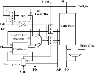
4. The Proposed DFT Scheme
In this section, we discuss a scheme for two-pattern testability of controller-data path circuits. We classify the paths and segments of a controller-data path circuits into following four groups:
Group1: RTL paths (explained in Section 2) of the data path excluding the paths those end at SLR.
Group2: RTL paths those end at SLR.
Group3: The paths that start at the PIs or the state register of the controller or at SLR and end at the POs or the state register of the controller or at CLR
Group4: Segments represented by register load lines and MUX select lines.
Our aim is to develop a scheme that ensures two- pattern testability for all these paths and segments. In the process of developing the scheme, we first transform the data path to an HTPT one by following the method of [6]. We further modify the data path to fulfill the requirements for the testability of the control segments (discussed in Section 3). Fig. 9 shows the detail of our scheme. The scan chain along the state register of the controller, the CLR and the SLR is an ES chain. A PI and a PO of the data path is shared for scan-in and scan-out ports of the ES chain, respectively. The test controller of Fig. 9 is a sequential circuit. The test controller consists of a test plan generator (TG) and a test plan index register (TIR). A TG generates a test plan (discussed in Section 2) i.e. a sequence of control vectors depending on the contents of the TIR. The length of the TIR is log2n where n is the number of required test plans to test the RTL paths of the data path. The input of the TIR is connected to a PI of the data path. We add three extra pins to the circuit. They are L/H, T/N and S/P. L/H is connected to the load enable signals of the TIR. An inversion of L/H is connected to the load enable signals of the CLR. The T/N pin is used to multiplex the control signals of the normal controller and the test controller. Also, in normal mode the T/N pin apply logic zero to the control signals of the added DFT
elements to the data path. The S/P pin is used to switch the ES chain from shift mode to parallel mode and vice versa. All these pins should be zero for normal circuit operation.
We now explain how the scheme can be used to test the paths and segments of the above mentioned 4 groups. Paths or segments of each group are tested separately. In the following we briefly discuss the procedure of testing the paths or segments of each group.
Group 1: First a test plan index is loaded to the TIR and then the TG generates the sequence of control signals necessary for that test plan. Test vectors are fed from the PIs and test responses are observed at a PO. Table 2 shows the required logic values for L/H, T/N, and S/P. The process is repeated for all the test plans.
Operation L/H(1/0) T/N(1/0) S/P(1/0)
Loading TIR 1 X X
Generating test plan 0 1 0
Group 2: The procedure of testing of the paths of this group is similar to the testing of the paths of group 1. However the test response is captured at SLR and then shifted out via the ES chain. Table 3 shows the required logic values for L/H, T/N, and S/P.
Operation L/H(1/0) T/N(1/0) S/P(1/0)
Loading TIR 1 X X
Generating test plan 0 1 0
Shifting out Test responses 0 X 1
Group 3: These paths are tested using the traditional ES approach. Test vectors are loaded to the ES chain and applied to the circuit by using shift operation. The test responses are captured in the ES chain and then shifted out for observation. Obviously the care bits for the test vectors span only the state register of the controller and the SLR. Table 4 shows the required logic values for L/H, T/N, and S/P.
Operation L/H(1/0) T/N(1/0) S/P(1/0)
Loading ES chain 0 X 1
Applying vectors 0 0 1
Capturing test response 0 0 0
Shifting out test response 0 X 1
Group 4: The methods of testing the segments of this group have been described in Section 2. In short, each segment is tested separately by using the hold and shift properties of the ES chain and by controlling the PIs of the data path with appropriate data. Table 5 shows the required logic values for L/H, T/N, and S/P for hold and shift operations.
Operation L/H(1/0) T/N(1/0) S/P(1/0)
Shift operation 0 X 1
Hold operation 1 X X
Table 2: Logic values for L/H, T/N, S/P
Table 3: Logic values for L/H, T/N, S/P
Table 4: Logic values for L/H, T/N, S/P
Table 5: Logic values for L/H, T/N, S/P
Data Path S
L R
C L R Controller
PI
TG T I R
1 0
To S_in
From S_out PI
S_out
S_in L/H
T/N
S/P PO PO
To added DFT elements
State registers
Test Controller
Fig. 9: The proposed DFT scheme
Controller Data Path Circuit
PI PO state status control area PI PO bit reg mod area
Paulin 0 0 6 0 16 86 32 32 16 7 4 6138
LWF 0 0 4 0 8 42 16 16 16 5 3 2120
Tseng 0 0 5 0 13 64 48 32 16 6 7 4573
RISC 0 2 11 54 61 580 32 96 32 40 19 59808
5. Experimental results
In this section we present experimental results to compare the area overhead incurred by our scheme with that of the enhanced scan approach. We applied our scheme to three benchmark circuits and a RISC processor provided by a semiconductor industry. The characteristics of these circuits are shown in Table 1. The columns
“Controller” and “Data Path” contain the characteristics of the controller part and the data path part respectively. The columns PI, PO and Area denote the numbers of primary inputs and primary outputs and area of respective parts. The areas are generated by logic synthesis tool Design Compiler (Synopsys). The columns “state”, “status” and
“control” in “Controller” denote the numbers of states, status inputs and control outputs respectively. The column
“bit”, “reg” and “mod” in “Data Path” denote the bit width of the data path and the number of registers and operational modules in the data path.
Area overhead (%) Circuit Bit-width
Enhanced-scan Our scheme
8 45.46 69.85
16 31.41 27.31
Paulin
32 19.32 10.4
8 66.97 89.45
16 64.47 48.75
LWF
32 63.25 29.5
8 46.76 64.23
16 36.3 27.73
Tseng
32 25.4 11.08
RISC 32 36.49 13.85
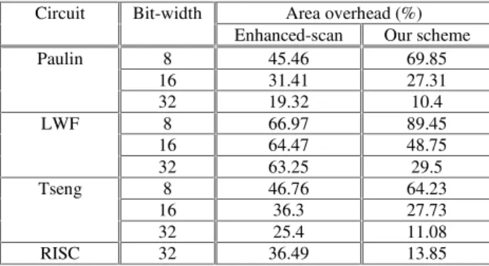
Table 7 presents the experimental results regarding area overhead. In both enhanced scan approach and our scheme, the area overhead decreases with the increase in bit-width of the data path. However, the rate of decrease is faster in our case. Area overhead incurred by enhanced scan approach is lower for 8-bit circuits. But, for 16-bit and 32-bit circuits our scheme results in lower area overhead.
5. Conclusions
In this paper we have introduced a scheme for two- pattern testability of a controller-data path circuit. This is
a hybrid scheme that makes use of both scan and non-scan techniques. The scheme is mainly based on path delay fault model. However the MUX select lines and register load lines are tested as RTL segments. The proposed scheme supports hierarchical test generation and can achieve fault coverage similar to the ES approach. In the context of hardware overhead, our approach is better for the circuits having data path of higher bit-width. In the present work, we added a test controller to the circuit. Our future work is to modify the data path in such a way that the need of the test controller can be eliminated.
Acknowledgements:
This work was sponsored in part by NEDO (New Energy and Industrial Technology Development Organization) through the contract with STARC (Semiconductor Technology Academic Research Center) and supported by Japan Society for the Promotion of Science (JSPS) under the Grant-in-Aid for Scientific Research and by Foundation of Nara Institute of Science and Technology under the grant for activity of education and research.
References:
[1] Angela Krstic and Kwang-Ting (Tim) Cheng, Delay Fault Testing for VLSI Circuits, Kluwer Academic Publishers, 1998.
[2] J. Savir, “On board-side delay testing”, Proc. of 12th IEEE VLSI Test Symposium, 284-290, 1994.
[3] K.-T. Cheng, S. Devdas and K. Keutzer, “Delay-fault test generation and synthesis for testability under a standard scan design methodology”, IEEE Transactions on Computer Aided Design Of Integrated Circuits and Systems, Vol. 12 No.8 pp. 1217-1231, 1993.
[4] B. I. Dervisoglu and G. E. Stong, "Design for testability: using scan path techniques for path-delay test and measurement", Proc. of Int. Test Conf., pp. 365-374,1991. [5] S. Dasgupta, R. G. Walther and T. W. Williams, “An
enhancement to LSSD and some application of LSSD in reliability, availability and serviceability”, Proc. of Fault Tolerant Computing Symp., FTCS-11., pp. 32-34, 1981. [6] M. A. Amin, S. Ohtake and H. Fujiwara, “Design for
hierarchical two-pattern testability of data paths”, Proc. Of IEEE 10th Asian Test Symposium, pp 11-16, 2001. [7] S. Ohtake, H. Wada, T. Masuzawa and H. Fujiwara, "A
non-scan DFT method at register-transfer level to achieve complete Fault efficiency", Proc. of the ASP-DAC, pp. 599- 604, 2000.
Table 7: Area overhead
Table 6: Circuit characteristics