Design for Testability of Software-Based Self-Test for Processors
Masato Nakazato†, Satoshi Ohtake†, Michiko Inoue†and Hideo Fujiwara†
† Graduate School of Information Science, Nara Institute of Science and Technology Kansai Science City, 630–0192, Japan
†E–mail:{masato-n, ohtake, kounoe, fujiwara}@is.naist.jp
Abstract
In this paper, we propose a design for testability method for test programs of software-based self-test using test program templates. Software-based self- test using templates has a problem of error mask- ing where some faults detected in a test genera- tion for a module are not detected by the test pro- gram synthesized from the test. The proposed method achieves 100% template level fault efficiency in a sense that the proposed method completely resolves the problem of error masking. Moreover, the pro- posed method adds only observation points to the original design, and it enables at-speed testing and does not induce delay overhead.
Key words:
software-based self-test, processor, test program template, design for testability, error masking
1. Introduction
In recent years, it has been essential that pro- cessors with high performance and rich functional- ity have accurate and at-speed testing. Though the full-scan approach is commonly used due to its sim- plicity, it induces performance penalty, area over- head and excessive power consumption. The built- in self-test (BIST), which is one of the other widely used techniques, uses embedded hardware, pseudo- random pattern generators and response analyzer, and applies test patterns to modules on the circuit at the normal operational speed. However, design modifications are required to make a circuit to be BIST-ready, and involve large amount of manual ef- fort. The BIST also induces area overhead. Further- more, an application of random patterns results in excessive power consumption.
A number of approaches [1-7] have been pro- posed for software-based self-test (SBST). In SBST, we test a processor by executing a sequence of in- structions called a test program. A processor can be tested by communicating with the memory, thus en- abling at-speed testing. Of course, we used commu- nication between the memory and the outside ATE as pre- and post-processor of the execution of the test program.
Some methods among the SBST methods gener- ate a test program based on test program templates
targeting structural faults to achieve the high fault coverage [3-7]. In this approach, gate-level test gen- eration is applied for each module under test (MUT) of a processor (MUT test generation), and a test program is synthesized from a test pattern gener- ated in MUT test generation (test program synthe- sis), where a test program justifies the test pattern from the memory to the MUT and propagates the test response from the MUT to the memory. To guarantee the test program synthesis, test program templates are used. A test program template is an instruction sequence with unspecified operands that delivers test patterns to an MUT and observes the test responses. The approach extracts constraints from each template since the template represents ways to propagate tests from the memory and test responses to the memory, and applies test generation for the MUT under such constrains. In this approach, we can easily synthesize a test program from a test pat- tern for the MUT. However, the justification and ob- servation parts consider only behavior of a fault-free processor and do not consider behavior of a faulty processor, and such parts do not work as expected. In this case, some faults detected by a test pattern for a MUT may not be detected by the synthesized test program. We call such a phenomenon “error mask- ing.”
In this paper, we propose a design for testabil- ity method that completely resolves the problem of error masking for any test programs generated by the template-based SBST approach. The proposed method adds only observation points to the original design, and it enables at-speed testing and does not induce delay overhead.
This paper is organized as follows. In Sections 2 and 3, we show a processor model and a test program generation using templates. In Section 4, we ana- lyze error masking and define template level fault ef- ficiency. In Section 5, we propose a design for testa- bility of SBST for processors and the experimental results are shown in Section 6. Finally, Section 7 concludes this paper.
2. Processor Model
A processor is specified by register transfer level (RTL) description. Figure 1 shows an example of a processor. In RTL description, the processor consists of combinational modules such as arithmetic logic 15th IEEE Asian Test Symposium (ATS'06), pp. 375-380, November 2006.
CM
CM CM CM
CM
Memory
CM : Combinational Module SM !Sequential Module SM
: Register
Figure 1. An example of a processor.
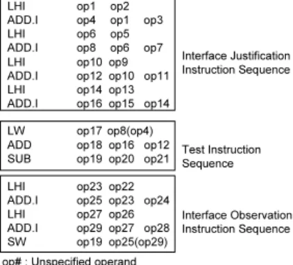
Interface Justification Instruction Sequence
Test Instruction Sequence
Interface Observation Instruction Sequence op# : Unspecified operand
LHI op1 op2
ADD.I op4 op1 op3
LHI op6 op5
ADD.I op8 op6 op7
LHI op10 op9
ADD.I op12 op10 op11
LHI op14 op13
ADD.I op16 op15 op14
LW op17 op8(op4) ADD op18 op16 op12 SUB op19 op20 op21
LHI op23 op22
ADD.I op25 op23 op24
LHI op27 op26
ADD.I op29 op27 op28 SW op19 op25(op29)
Figure 2. An example of a template. unit (ALU) or multiplexer (MUX), sequential mod- ules such as a controller specified as a finite state machine, a signal (an RTL signal) that connect the modules, and buses. A bus constructed by a tri-state buffer is a tri-state bus[11], and we assume that each output of the tri-state bus has a masking circuit that makes a logic value (‘0’ or ‘1’) to prevent a high impedance. For a fault-free processor, we also as- sume the following about inputs and outputs of a tri- state bus.
(1) Two or more inputs of a tri-state bus are not ac- tivated simultaneously.
(2) An output of a tri-state bus is masked into a spec- ified logic value if any input of the tri-state bus is not activated.
A processor is assumed to be synthesized while preserving the hierarchy of the modules, and there- fore each module can be identified in a gate-level de- scription.
3. Test Program Generation based on Templates
We first explain a test program generation using test program templates. In the rest of this paper, we call a test program template a template. Figure 2 shows an example of a template, which consists of three sequences: an interface justification instruction sequence, a test instruction sequence and an interface observation instruction sequence. An interface justi- fication instruction sequence justifies test patterns to registers which are adjacent to inputs of MUT. A test
instruction sequence applies test patterns to the MUT and propagates a test response to registers that are adjacent to outputs of MUT or the memory. An in- terface observation instruction sequence propagates the test response stored in registers to the memory. A test program synthesized by using templates can jus- tify test patterns to inputs of the MUT and observe the test responses if a processor operates correctly; that is, if the processor is fault-free. For each tem- plate, we extract constraints about the input space and the output space of the MUT and perform MUT test generation under constraints. Kambe et. al.[5] proposed an efficient method to extract such a con- straint as a constraint circuit from each template, where the inputs of a constraint circuit correspond to the operands of a template. In an MUT test gener- ation, we perform a test generation for a circuit that is connected the MUT with the constraint circuit. We can directly transform test patterns obtained by MUT test generation into operands of the template and eas- ily synthesize a test program.
4. Error Masking
In this section, we define template level fault effi- ciency which is utilized for evaluation of error mask- ing analyze error masking.
4.1. Template Level Fault Efficiency
In the test program generation method using tem- plates, interface justification instruction sequences, and interface observation instruction sequences are generated only in consideration of the behavior of the fault-free processor. When applying a test pro- gram to the processor, errors may appear during ex- ecution of these sequences. Therefore, we cannot guarantee that the test program will justify test pat- terns to the MUT, or observe the test response. This means that some faults detected in the MUT test gen- eration may not be detected by the test program syn- thesized from the test. We call this situation “error masking.” In this paper, we define template level fault efficiency (FET) as measure to evaluate for er- ror masking as follows.
FET= #T P
#MT,
where #MT is the number of faults detected in the MUT test generation and #T P is the number of faults detected by the test program among the #MT faults. A template level fault efficiency 100% means that there is no error masking.
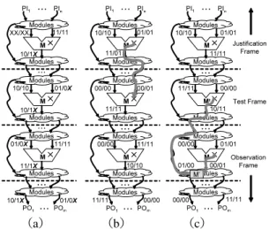
4.2. Analysis of Error Masking
Figure 3 shows examples of error masking us- ing a time frame expansion model during execution of a test program. Each time frame corresponds to 1 clock. In the time frame expansion model, time frames that apply test patterns to the MUT are called a test frame, while time frames corresponding to the time before the test frame are called a justification
PI PI
!!!
M Modules
XX/XX 11/11
10/1X Modules
Modules
!!!
10/10 01/0X
M 10/1X
Modules
Modules
!!!
01/0X 11/11
M 11/1X
Modules
Modules
!!!
PO PO
!!!
10/1X 01/0X
(a)
PI PI
!!!
M Modules
Modules
Modules!!!
M Modules
Modules!!!
M Modules
Modules!!!
PO PO
!!!
10/10 01/01
11/01
00/01 00/00
11/11
00/00 11/11
10/10
11/11 00/00
(b)
PI PI
!!!
M Modules
Modules
Modules!!!
M Modules
Justification Frame
Test Frame
Modules!!!
M Modules
Observation Frame
Modules
!!!
PO PO
!!! M’
10/10 01/01
11/11
11/11 00/00
10/11
01/00 00/01 01/01 00/00
00/00 11/11
(c) Figure 3. Examples of error masking:(a) un- known values are propagated to any RTL sig- nal; (b) errors reach the MUT; (c) errors which are propagated to two RTL signals and meet at some module in some frame.
frame and time frames corresponding to the time af- ter the test frame are called an observation frame. The following situations can be considered as causes of error masking.
Figure 3 (a) shows an example of error masking induced by an unknown value. In the example, un- known values ‘Xs’ are propagated to some RTL sig- nals. In this figure, we describe the value of RTL sig- nal as “the value in fault-free circuit/value in faulty circuit.” In this case, the test pattern is delivered from the memory to MUT in the test frame through MUT in the justification frame. In a fault-free cir- cuit, specified values are propagated to the output of MUT in the justification frame even though these ap- pear ‘Xs’ at some inputs of MUT. On the other hand,
‘Xs’ appear at the output of MUT in the justification frame in the faulty circuit. The unknown values ‘Xs’ are propagated to the input of MUT at the test frame and fail to activate the fault at the frame.
Figure 3 (b) shows an example of error masking induced by a cycle. In the example, errors reach the MUT M. In this case, there is a cycle that includes M. The fault in M is activated at the justification frame, and then an error appears at some bit of the output of M. The error reaches some bit of the input of M in the test frame. Thus, the fault in M is not activated.
Figure 3 (c) shows an example of error mask- ing induced by the reconvergence of errors. In the example, errors are propagated to two RTL signals and meet at some module in some frame. A fault in the MUT is activated in both the test frame and some observation frame. These errors are propa- gated through RTL signals and meet at some module M′ in some frame. The multiple errors mask each other in M′and no error is propagated to the output of M′. The situation in Figure 3 (c) may occur if
there are reconvergent paths between the MUT and some module.
Let M and M′ be modules. We call a set of n- reconvergent paths from M to M′an n-reconvergent structure. Among the modules in an n-reconvergent structure S from M to M′and have only one path to M′, the furthest module from M′is called a reconver- gent point of S.
5. Design for Testability of Software- Based Self-Test
In this section, we propose a design for testability in order to avoid error masking.
5.1. Formulation
The proposed method avoids error masking dur- ing execution of a test program by adding the follow- ing functions to the original design.
• A function to initialize the value of all the reg- isters to ‘0’ or ‘1’
• A function to observe some RTL signals Since an advantage of SBST is the possibility of at-speed testing, it is important that the processor af- ter the DFT also enables at-speed testing. There- fore, we capture the values of the RTL signals to be observed at normal operational speed. We use a multiple input signature register (MISR) to capture the values of the RTL signals at normal operational speed. The proposed method adds only observation points to the original design; it enables at-speed test- ing and does not induce delay overhead.
We formulate the design for testability problem in order to avoid error masking as an optimization problem as follows.
Input: An RTL description of a processor
Output: An RTL description of an augmented pro- cessor that can achieve 100% template level fault efficiency
Objective: Minimizing the sum of the bitwidths of the RTL signals made observable
5.2. Sufficient Conditions for Avoiding Error Masking
We assume the following conditions for a test pro- gram.
• The value stored in the memory cell for which address is referred to during execution of the test program is known. In the fault-free proces- sor, unknown values are not propagated from the memory to the processor.
• The memory cell referred to during execution of the test program is initialized to a different value from the expected value, which will be stored in the memory cell during execution of the test program.
In this paper, we consider that a fault in a pro- cessor is detected if no value or an incorrect value is stored in some memory cell where the test pro- gram should write some expected value. If the test program fails to read a value from the memory cell
designated in the test program because of a fault, we consider such incorrect behavior results in the fail- ure to write the expected value to some designated memory cell in the test program; hence, faults can be detected.
To guarantee that the proposed method can achieve 100% template level fault efficiency, we show the sufficient condition for a processor such that error masking does not occur during execution of the test program obtained by the test program syn- thesis using test program templates.
Theorem 1 Error masking does not occur during execution of a test program if a processor satisfies the following three conditions.
(1) Each register in the processor has a function that initializes the value of the register to ‘0’ or ‘1’, and all the control signals of each tri-state bus and all the control signals of its masking cir- cuits are observable.
(2) For each cycle, at least one RTL signal on the cycle is observable.
(3) For each n-reconvergent structure S, there exist a set P of n− 1 reconvergent paths in S, such that at least one RTL path is observable for each path in P.
Proof:
Let f be a stuck-at fault detected by a test program obtained by test program synthesis using test pro- gram templates. We consider the execution of a test program for f . Let M be a module with f .
First we show that a fault in a module of a proces- sor is detected during execution of the test program or the value of any RTL signal of the processor is not unknown.
If the fault is not detected, the values are read from the same memory addresses in both correct and faulty processors. Therefore, unknown values are not propagated from the outside of the processor. Moreover, if the fault is not detected, an error is not propagated to a control signal of a tri-state buffer in a tri-state bus, and the value is read from the tri-state bus in the correct operation when the value of the tri-state bus is transferred to a RTL signal connected to the tri-state bus. Then, if none of the inputs of the tri-state bus are activated, a logic value is trans- ferred from the masking circuit of the tri-state bus to the outputs of the tri-state bus in the fault-free pro- cessor, since the output value of the tri-state bus is masked to the logic value. The data transfer in the fault-free processor is also performed in the faulty processor since the error is not also propagated to the control signal of the masking circuit and of the tri- state buffer in the tri-state bus. Therefore, the value of each register next time is set to the value of the RTL signal at present time which is connected to a register, a primary input, and a tri-state bus that is not activated. Since the values of all the registers in the processor are initialized to the logic value at the start of the test program from condition (1), unknown val- ues are set to all the registers during execution of the test program.
Suppose the test program justifies a test pattern to the inputs of M at time t in the fault-free processor. When the interface justification instruction sequence
and the test instruction sequence are executed, we indicate that the test pattern for f reaches the inputs of M at time t or f is detected until time t.
We think that the test pattern of f does not reach the inputs of M at time t. We consider the bits of the register with the specified value (‘0’ or ‘1’) in or- der to justify this test pattern in the correct operation of the processor. A different value from the correct value is propagated to a bit b, which is one of these bits, since the test pattern for f does not reach inputs of M. The value of b is error since the register is set known values during execution of the test program. Since an error only occurs at M, a path P through b from an output of M to an input of M exists and the error is propagated on the path. For each cycle, since an RTL signal on the cycle is observable from con- dition (2), an RTL signal on P is observable and the fault is detected. Therefore, f is detected until time tor the test pattern for f reaches the inputs of M.
If the test pattern of f reaches inputs of M at time t, then f is activated and an error appears an output of M. The output of M at time t can be observed at a primary output in the fault-free processor. There- fore, a path such that an error is propagated from M to an primary output (an error propagation path) ex- ists. Suppose the fault is not detected. In this case, an error is not propagated to a primary output. If the error is not propagated to a primary output, a mod- ule M′such that the error is prevented to propagate on the error propagation path exists. For a module without faults on the error propagation path, if the error is only propagated to the inputs of the module, the error is propagated to the outputs of the module. Therefore, M′is M or the error is propagated to the inputs of M′, which is not on the error propagation path. If M′is equal to M, the error is propagated on a cycle. In condition (2), the error is observed and the fault is detected. If the error is propagated to the inputs of M′, which is not on the error propagation path, the error is propagated on all the reconvergent paths of two-reconvergent structure from M to M′. Since an RTL signal on either of the two reconver- gent paths is observable due to condition (3), the er- ror is observed and f is detected.
Therefore, a fault f detected by MUT test gener- ation can detect during execution of a test program synthesized from the test pattern for f .
5.3. Algorithm
We propose an algorithm such that a processor satisfies the sufficient condition proposed in subsec- tion 5.2. This algorithm consists of the following five steps.
Step 1: A function to initialize the value of each register in the processor to ‘0’ or ‘1’ is added, and all the control signals of each tri-state bus and all the control signals of its masking circuits are made observable.
Step 2: The circuit graph of the processor is gener- ated.
Step 3: For each MUX in the processor, removing the edge of the circuit graph corresponding to the control signal of the MUX.
Step 4: For each cycle in the circuit graph, at least one RTL signal on the cycle is made observable. Step 5: For each n-reconvergent structure S, at least one RTL signal on each reconvergent paths in S is made observable.
We describe the details of the algorithm as fol- lows.
Step 1: A function that initializes the value of the register to ‘0’ or ‘1’ is added to each register in the processor. This initializing function is control- lable from a primary input and sets the initial speci- fied value in the register at the time of the start of a test program. Since, in general, the processor needs some controls from the exterior of the processor, a primary input utilized for initializing the registers is shared with the primary inputs utilized for starting a test program. Therefore, it is not necessary to add a new primary input.
Step 2: A circuit graph is generated from the RTL description of the processor. The circuit graph is ex- pressed in a directed graph G= (V,E), where v ∈ V is a vertex corresponding to a combinational module, a sequential module, a register, a primary input and a primary output and e ∈ E is an edge corresponding to an RTL signal. The edge of the circuit graph has the weight. The weight corresponds to the bitwidth of the RTL signal.
Step 3: For each MUX in the processor, we remove the edge of the circuit graph corresponding to the control signal of the MUX from the circuit graph. Here, removing the edge of the circuit graph means observing the RTL signal corresponding to the edge. In n-reconvergent structure such that an MUX corre- sponds to a reconvergent point, error masking does not occur even if errors propagate to inputs (data in- puts) except for the control input (the signal for se- lecting a data input) of the MUX. Therefore, by ob- serving the control input of the MUX instead of con- dition (3) in subsection 5.2, error masking does not occur in such reconvergent structure. In general, the bitwidth of RTL signals on paths which reach data inputs of the MUX is larger than that on paths which reach the control input of it. We can reduce the hard- ware overhead to observe the RTL signal connected with the control input of the MUX.
Step 4: In this step, we search a set, which includes an RTL signal on each cycle in the processor, of RTL signals such that the sum of the bitwidths of RTL signals in the set is minimum. We perform the fol- lowing four steps in order to search such a set. Step 4.1: We search a cycle C such that the sum of the weight of edges is minimum by using the algo- rithm in [8]. Let ECbe a set of edges that construct the cycle C. For each edge ei∈ EC, if the weight of eiis minimum in EC, eiis removed from the circuit graph and added to a set Erof edges. C is added to a set Cminof cycles. This process is repeated until the circuit graph becomes acyclic.
Step 4.2: Let Ecut be a set of edges corresponding to the observing RTL signals. For each edge ei∈ EC of each cycle C ∈ Cmin, if the number of cycles which include eiis maximum and the weight of eiis minimum, eiis added to Ecut. If eiis in a member of Er, a member of Ercorresponding to eiis removed.
Table 1. Characteristics of processors
Processor #Gate #Register #Module #Instruction
SAYEH 6141 12 10 29
Dlx N 34032 50 95 25
If eiis not in a member of Er, eiis removed from the circuit graph. C is removed from Cmin. This process is repeated until Cminbecomes empty. If Erdoes not become empty, all edge in Erare added to the circuit graph.
Step 4.3: Step 4.1 and 4.2 are repeated until the cir- cuit graph becomes acyclic.
Step4.4: If some of the edges in Ecut obtained by processing from Step 4.1 to Step 4.3 is added to the circuit graph, the circuit graph may not become acyclic. For each ec∈ Ecut, if the circuit graph be- comes acyclic when ecis added to it, ecis removed from Ecut and ecis added to the circuit graph. Step5: Let PSbe a set of n − 1 reconvergent paths in each n-reconvergent structure S such that the MUX is not the reconvergent point. We search a set, which includes an RTL signal corresponding to an edge of the minimum weight on each p ∈ PS, of RTL signals such that the sum of the bitwidths of RTL signals in the set is minimum. We perform the following three steps to search such a set.
Step5.1: For a pair of vertices viand vj(vi̸= vj) of the circuit graph, if vjcorresponds to the MUX, we extract all the paths from vito vjand let Pi,jbe a set of such paths.
Step5.2: For a pair of paths p!and pmin Pi,j, let ec
be an edge such that the weight of an edge on either p!or pmis minimum. The path that includes ecis removed from Pi,j. ecis added to Ecut and removed from the circuit graph. This process is repeated until the number of members in Pi,jbecomes one. Step5.3: Steps 5.1 and 5.2 are repeated for all pairs of vertices in the circuit graph.
As the result of processing these steps, we ob- serve RTL signals corresponding to edges in Ecut. These RTL signals are connected to an MISR. 6. Experimental Results
We evaluate the proposed method using a non- pipelined processor SAYEH[9] and a five-stage pipelined processor Dlx N that is based on Dlx processor[10]. Table 1 shows the characteristics of SAYEH and Dlx N. The column titled “#Gate” de- notes the number of primitive gates. The column headed “#Register” and “#Module” denote the num- ber of registers and the number of modules at RTL in the processor, respectively. The column “#Instruc- tion” denotes the number of instructions defined in an instruction set architecture (ISA). The numbers of gates in SAYEH and Dlx N processor are 6,141 and 34,032, respectively. The numbers of registers and modules at RTL in both processors are 12 and 50, and 10 and 95, respectively. Both processors have the standard 29 and 25 instructions, respectively.
Table 2 shows hardware overhead of the proposed method and the full-scan design for SAYEH and
Table 2. The number of observable bits and hardware overhead
Processor DFT Area HOH(%)
Original Additional #OB
SAYEH full-scanProp. 12389 14853306 165114 11.9926.68 Dlx N full-scanProp. 58696 136357917 1379273 23.2313.49
Dlx N. The column “DFT” denotes the design for testability method applied to both processors. In the column “DFT,” “full-scan” and “Prop.” denote the full-scan design method and the proposed method, respectively. The columns “Area” and “HOH” de- note the area of the processor and the hardware over- head, respectively. In the column “Area,” “Original” and “Additional” denote the original area of the pro- cessor without DFT and the additional area that in- creases by applying DFT method to the processor, respectively. The column “#OB” denotes the number of observable bits. In the full-scan design method and the proposed method, an observable bit means the number of scan flip-flops and the number of in- puts of MISR. The number of observable bits of the proposed method becomes less than that of the full- scan design method for both processors. For Dlx N processor, the hardware overhead of the proposed method is smaller than that of the full-scan design method. The Dlx N processor has many registers in- cluding the architecture registers appear in ISA and the pipeline registers to enhance the performance. Therefore, the full-scan design induces a large area overhead. However, for the SAYEH processor, the hardware overhead of the proposed method is larger than that of the full-scan design method. This is because that the SAYEH processor has a very area- optimized design with a lot of loops and a few reg- isters; therefore, the proposed method needs many observation points whereas full-scan design requires little area overhead. Moreover, the hardware over- head per one observed bit of the proposed method is larger than for the full-scan design, since we es- timate the hardware overhead as the area of MISR with the same number of bits as the observed bits. However, this hardware overhead can be reduced if we compress the observed space before applying it to MISR.
7. Conclusions and Future Work In this paper, we proposed a design for testabil- ity method of software-based self-test for proces- sors. We proved that the proposed method can achive 100% template level fault efficiency if a processor satisfies three conditions: (1) each register in the pro- cessor has a function that initializes the value of the register to ‘0’ or ‘1’; and all the control signals of each tri-state bus and all the control signals of its masking circuits are observable, (2) for each cycle, at least one RTL signal on the cycle is observabl;, (3) for each n-reconvergent structure S, there exist a set Pof n − 1 reconvergent paths in S such that at least one RTL path is observable for each path in P. The
experimental results reveal that the proposed method achieves less hardware overhead than full-scan de- sign if the processor features many registers and less loops or reconvergent paths. In general, modern pro- cessors oriented to high performance have many reg- isters to accelerate their speed, while the structure tends to be simpler than the design oriented to area optimization. From this observation, we consider that the proposed method is suitable for such modern processors. Since the proposed method adds only observation points to the original design, it enables at-speed testing and does not induce delay overhead. Further reduction of hardware overhead ,and evalu- ations of the test application time and the fault ef- ficiency are issues to be investigated in our future work.
Acknowledgment The authors would like to thank Dr. Tomokazu Yoneda, and other members of Computer Design and Test Laboratory of Nara Institute Science and Technology for their valu- able discussions. This work was supported in part by joint research with Semiconductor Tech- nology Academic Research Center (STARC), in part by 21st-Century COE Program and in part by Japan Society for the Promotion of Science (JSPS) under Grants-in-Aid for Scientific Research B(2)(No. 15300018), under Grants-in-Aid for Scien- tific Research C(No. 18500038) and for Young Sci- entist(B)(No. 17700062).
References
[1] W. -C. Lai, A. Krtic and K. -T. Cheng, “Test program syn- thesis for path delay faults in microprocessor cores,” Proc. of International Test Conference 2000, pp. 1080-1089, 2000. [2] W. -C. Lai, A. Krtic and K. -T. Cheng, “Instruction-Level
DFT for testing processor and IP cores in system-on-a chip,” Proc. of Design Automation Conference 2001, pp. 59-64, 2001.
[3] L. Chen and S. Dey, “Software-based self-testing method- ology for processor cores,” IEEE Trans. on CAD,, vol. 20, no. 3, pp. 369-380, 2001.
[4] L. Chen, S. Rabi, A. Raghunath and S. Dey, “A scalable software-based self-test methodology for programmable processors,” Proc. of Design Automation Conference 2003, pp. 548-553, 2003.
[5] K. Kambe, M. Inoue and H. Fujiwara, “Efficient template generation for instruction-based self-test of processor cores,
” Proc. of IEEE 13th Asian Test Symposium (ATS’04), pp. 152-157, 2004.
[6] S. Yokoyama, K. Kambe,M. Inoue,H. Fujiwara,“Effi- cient generation of instruction templates for pipeline proces- sor self-test, ” Technical Report of IEICE (DC2004-58), Vol. 104, No. 478, pp.61-66, Dec. 2004. (In Japanese). [7] M. Inoue, K. Kambe, N. Hoashi, and H. Fujiwara,
“Instruction-Based Self-Test for sequential modules in pro- cessors,” Proc. of IEEE 5th Workshop on RTL and High Level Testing (WRTLT’04), pp. 109-114, 2004.
[8] M. N¨aher, “LEDA,” Cambridge university press, 1999. [9] Z. Navabi, “VHDL Analysis and Modeling of Digital Sys-
tems,” McGraw-Hill, 1997.
[10] J. H. Hennesy and D. A . Patterson, “Computer Architec- ture: A Quantative Approach,” Morgan Kaufmann Publish- ers, 1996.
[11] Semiconductor Technology Academic Research Center (STARC), “RTL design style guide,” STARC, 2000. (In Japanese).
![I, §3] that the Schur functionsλ(x1](data:image/gif;base64,R0lGODlhAQABAIAAAP///wAAACH5BAEAAAAALAAAAAABAAEAAAICRAEAOw==)