Article
A High-Efficiency Voltage Equalization Scheme for
Supercapacitor Energy Storage System in Renewable
Generation Applications
Liran Li, Zhiwu Huang *, Heng Li and Honghai Lu
School of Information Science and Engineering, Central South University, 22 South Shaoshan Road,
Changsha 410000, China; [email protected] (L.L.); [email protected] (H.Li); [email protected] (H.Lu)
* Correspondence: [email protected]; Tel.: +86-731-8253-9616
Academic Editor: Andreas Sumper
Received: 2 April 2016; Accepted: 8 June 2016; Published: 13 June 2016
Abstract: Due to its fast charge and discharge rate, a supercapacitor-based energy storage system is especially suitable for power smoothing in renewable energy generation applications. Voltage equalization is essential for series-connected supercapacitors in an energy storage system, because it supports the system’s sustainability and maximizes the available cell energy. In this paper, we present a high-efficiency voltage equalization scheme for supercapacitor energy storage systems in renewable generation applications. We propose an improved isolated converter topology that uses a multi-winding transformer. An improved push-pull forward circuit is applied on the primary side of the transformer. A coupling inductor is added on the primary side to allow the switches to operate under the zero-voltage switching (ZVS) condition, which reduces switching losses. The diodes in the rectifier are replaced with metal-oxide-semiconductor field-effect transistors (MOSFETs) to reduce the power dissipation of the secondary side. In order to simplify the control, we designed a controllable rectifying circuit to achieve synchronous rectifying on the secondary side of the transformer. The experimental results verified the effectiveness of the proposed design.
Keywords: voltage equalization; supercapacitor; energy storage systems; renewable generation applications
1. Introduction
In recent years, a growing interest has been seen in renewable generation systems; the most common renewable energy sources are solar and wind energy [1]. The naturally intermittent properties of wind speed and sunlight cause power fluctuations in wind turbines and photovoltaic systems, so it is difficult to store the renewable energy for future use [2]. Thus, an energy storage system (ESS) is needed in renewable generation systems to manage the power flow [3].
Conventionally, there are two popular ESSs for renewable generation systems: batteries and supercapacitors [4,5]. Batteries feature location flexibility and scalable capacity, which make them a suitable ESS technology for integration with renewable generation systems [6,7]. A major drawback of batteries is their slow dynamics. Because the power output is heavily weather dependent and changes rapidly, the battery lifetime and state-of-charge (SOC) are greatly degraded [8]. A promising new ESS technology is to use supercapacitors, which have excellent characteristics, such as a large power density, fast charge/discharge rate, high efficiency and a long cycle life [9–11].
Because of the relatively low voltage and capacity of a supercapacitor cell, hundreds of supercapacitors are typically connected in series to satisfy the large voltage and power requirements of renewable generation applications. When multiple supercapacitors are connected in series, the cell imbalance is a serious problem [12,13]. The cell imbalance of supercapacitors is typically caused by
manufacturing and environmental factors [14–16]. In an unbalanced supercapacitor ESS, cells with a small capacity may be overcharged or over-discharged during operation, which is harmful to the system [17,18]. In order to ensure the safety of the ESS while improving its efficiency, the voltage needs to be actively equalized [19].
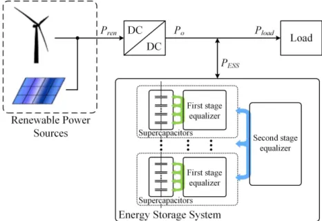
There are many papers [20–24] concerned about the renewable energy storage system. Figure1 shows the typical structure of the supercapacitor ESS in a renewable generation system.
Figure 1. The structure of the supercapacitor energy storage system (ESS) in renewable generation systems.
In [20], the authors presented an original control algorithm for a hybrid energy system with a renewable energy source. A supercapacitor module functioned by supplying energy to regulate the DC-bus energy, and the fuel cell supplied energy to the supercapacitor module in order to keep it charged. The literature [21] presented a power smoothing strategy based on a supercapacitor for power conditioning of distributed renewable generation. The power smoothing controller generated the power reference for the DC/DC converter, which has a power tracking control implemented with sliding-mode techniques. In [22], the authors presented a method of improving battery lifetime in a small-scale remote-area wind-power system by the use of a battery/supercapacitor hybrid energy storage system. The supervisory control algorithm and hardware implementation were described, and the projected long-term benefits of the proposed system were assessed by simulation. In [23], a hybrid control strategy was designed and analyzed for a hybrid energy storage system (HESS). In the proposed method, batteries were used to balance the slow changing power surges, whereas supercapacitors (SC) were used to balance the fast changing power surges. In [24], the authors considered a renewable energy hybrid power plant, fed by photovoltaic (PV) and fuel cell (FC) sources with a supercapacitor (SC) storage device. They designed an intelligent fuzzy logic controller based on the flatness property for DC grid voltage regulation, and the authors proposed a simple solution to the fast response and stabilization problems in the power system.
These studies investigated different aspects of the supercapacitor energy storage system in renewable generation applications. However, they did not consider the voltage equalization of supercapacitors in the application. In fact, the voltage equalization is an important topic in supercapacitor applications.
modules. The first-stage and second-stage equalizers can be designed to share the same circuit topology. This modular design method can reduce the complexity and voltage stress of equalizers. Moreover, a modular supercapacitor ESS is scalable and easy to maintain [26].
In renewable generation applications, supercapacitors are usually used to deal with the quick power fluctuations [27]. Thus, the ESS is charged and discharges very rapidly [21], which places severe demands on the voltage equalizer. The system needs to supply a large equalization current to equalize the voltage in a short amount of time. Moreover, with the increased equalization current, the equalization circuit needs to be at a high level of efficiency. Hence, both the equalization rate and equalization efficiency should be considered in the design.
Generally, existing voltage equalization schemes can be divided into two categories,i.e., the passive scheme and the active scheme. In the passive scheme, a resistor is connected in parallel with a supercapacitor cell to absorb the extra energy [28]. The implementation of the passive scheme is simple and inexpensive, with lower efficiency due to the involvement of lossy resistors. The passive voltage balancing schemes are usually used for low power applications.
In the active scheme, the energy is transferred among supercapacitor cells with the help of power converters. As compared to the passive circuit-based approaches, higher efficiency can be achieved in the active voltage balancing circuits, since less loss is generated by the voltage balancing circuits. There are two types of energy transfer modes, which are cell to cell mode [29] and stack to cell mode [30,31] in an active cell balancing circuit.
The stack-to-cell mode is more suitable for the supercapacitor energy storage system in renewable generation applications, as a higher equalization current can be provided. An equalizer based on an isolation voltage converter is a common equalization scheme [30,31]. However, the use of a diode rectifier circuit will generate very large energy losses in the condition of high equalization current. Therefore, they are not suited for renewable generation applications.
In this paper, we present the design of a rapid and efficient supercapacitor voltage equalization scheme for renewable energy applications. We propose an improved isolated converter topology that uses a multi-winding transformer. This topology can transfer the energy from the supercapacitor stack to weak cells in order to produce a higher equalization current and rapidly equalize the voltage of supercapacitors to satisfy the application requirements. An improved push-pull forward circuit is applied on the primary side of a transformer. A clamping capacitor is added to reduce the peaking voltage and to improve the equalization current, which eventually improve the voltage equalization rate. In order to improve the efficiency of the equalizer, a coupling inductor is added on the primary side to allow the switches to operate under the zero-voltage switching (ZVS) condition, thereby reducing switching losses. Diodes in the rectifier are replaced with metal-oxide-semiconductor field-effect transistors (MOSFETs) to reduce the power dissipation of the secondary side; this significantly improves the rectifier efficiency. In order to simplify the control, we designed a controllable rectifying circuit to achieve synchronous rectifying of the secondary side of the transformer. A prototype was built to verify the equalization performance.
The contribution of this paper is two-fold. Firstly, an improved voltage equalization circuit is designed by considering the intermittent and volatility characteristics of renewable energy systems. The proposed equalization circuit based on the ZVS push-pull forward and zero current detection (ZCD) rectifying circuit can supply a large equalization current, which can achieve the rapid voltage equalization of supercapacitors. Secondly, the previous equalization schemes suffer a large power loss in rectifying diodes with heavy current. We propose a controllable rectifying circuit with MOSFETs to reduce the power dissipation of the secondary side. A coupling inductor is added on the primary side, which allows the switches to operate under the zero-voltage switching (ZVS) condition to reduce switching losses. All improvements are helpful to improve the energy transfer efficiency.
2. Voltage Equalizer Design
2.1. Schematic
Figure 2 shows the proposed voltage equalizer circuit, where C1,C2, ...,Cn is n series
supercapacitors in a stack andIchis the terminal current. When supercapacitors are being charged by
renewable sources,Ichis positive; when supercapacitors are discharging,Ichis negative.
Figure 2.The proposed voltage equalization circuit schematic.
An improved push-pull forward topology with clamping capacitors is used on the primary side of the transformer. The input voltage of the converter is used as the voltage of the supercapacitor stack. The improved push-pull forward topology adds a clamping capacitor to the traditional push-pull converter. This clamping capacitor can absorb the energy of the leakage inductance and feedback to the input, so the peak voltage can be constrained when the main switchesS1,S2turn off and the switch requirement is lowered. Applying clamping capacitors couples the two windings of the primary side. When the equalizer is working, the two windings of the primary side transmit energy to the secondary side at the same time. In other words, two forward converters transmit energy to the secondary side in parallel to increase the output current of the equalization circuit. By adding the coupling inductances L1andL2to the primary side, the switches of the primary side are turned on under the ZVS condition, which decreases the switching loss.
with low internal resistance to replace the ordinary rectifier diodes. This increases the equalization current and decreases the loss of the rectifier.
For the sake of simplicity, the following assumptions were made.
(1) There arensupercapacitor cells in a stack, where the cell capacitance isCk(k=1, 2, ...,n)and
the cell voltage isuk(k=1, 2, ...,n). The stack voltageustackis constant within a single switching period.
(2) The turn ratio of the multi-winding transformer is K = Np/Ns. The multi-winding
transformer has two primary windings, whereNp1=Np2=Np, andnsecondary windings, where
Nsk = Ns(k=1, 2, . . . ,n). The magnetizing inductance and leakage inductance of the transformer
are ignored.
(3) The coupled inductors compriseL1andL2. The equivalent inductance of coupled inductors is Leq=L+M, whereLis the self-inductance of the inductors andMis the mutual inductance between
L1andL2. The equivalent inductances ofL1andL2are equal, whereLeq=Leq1=Leq2.
(4) The voltage of the clamp capacitorCsis equal to the stack voltageustackin the steady state.
(5) The switches and diodes are ideal.
Figure3shows key waveforms of the proposed equalization circuit in the steady state, where Vgs are the corresponding driving signals ofS1andS2,Vds1is the drain-source voltage ofS1,Vds2is the drain-source voltage ofS2,VL1 is the voltage across the inductorL1,VL2 is the voltage across the inductorL2,ip1andip2are the winding currents of the transformer on the primary side andieqis the
equalization current supplied to the supercapacitor cell.
Figure 3.Key waveforms of the proposed voltage equalization circuit.
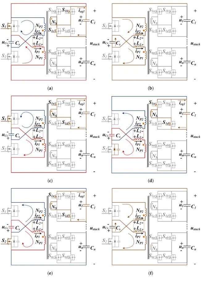
Suppose that the supercapacitorC1is the cell with the lowest voltage and that the rectification circuit connected toC1works first. There are six modes within one switching period. Figure4shows the equivalent circuit of each mode.
(a) (b)
(c) (d)
(e) (f)
(g) (h)
Figure 4.The operation modes of the equalizer circuit. (a) Mode 1:t0<t<t1; (b) timet1; (c) Mode 2:t1 <t <t2; (d) Mode 3:t2 <t <t3; (e) Mode 4:t3<t<t4; (f) timet4; (g) Mode 5:t4 <t<t5; (h) Mode 6:t5<t<t6.
The corresponding currents can be calculated as follows:
ip1(t) =ip1(t0) +
ustack+K·u1
Leq (
t−t0);
ip2(t) =ip2(t0) +
uCs+K·u1
Leq (t
−t0);
;t∈[t0,t1] (1)
During this process, the balancing currentieq1drops to zero whenip1 =−ip2. S1bandS1care
turned off att1.
Mode 2 (t1−t2: Figure4c): As shown in Figure4b, the primary current isip1=−ip2at timet1. At this point, the current throughS1is zero. The primary windings of the transformer are connected in series with the clamping capacitor. The primary current flows through the pathUstack+→Np2→ Cs→Np1→Ustack−. It is called the circulating currentIa, whereIa =ip1=−ip2.
After the timet1, the stack voltage and clamping capacitor voltage are added to the primary windingsNp1andNp2, respectively. The currentip1increases linearly. The currentip2changes from negative to positive. Energy is transferred to the secondary side.
The secondary windingNS1generates an induced voltage. The switchesS1a andS1dturn on
quickly. The equalization current of the secondary sideieqincreases and charges the supercapacitorC1. When the switchesS1aandS1dturn on, the voltage of the secondary side is clamped at the voltage
u1. Because the turn ratio of the transformer isK, the voltage of the two primary windings isKu1. The current flowing through the primary windings is given by:
ip1(t) =Ia+ustack
−K·u1 Leq (t
−t1);
ip2(t) =−Ia+
uCs−K·u1
Leq (t
−t1);
;t∈[t1,t2] (2)
At the timet2, the equalization current of the secondary sideieqreaches its maximumieqmax:
ieqmax=2K(ustack−K·u1)·(t2−t1)/Leq (3)
voltage, andS2turns on. The leakage energy of the coupled inductorL1is absorbed by the clamping capacitor. The coupled inductorL2also releases leakage energy to the supercapacitor stack throughS2. Meanwhile, the currentip1of the primary windings decreases quickly, andip2decreases to zero and then reverses to quickly increase. The equalization current of the secondary sideieqdecreases quickly.
During this process, the current flow though the two primary windings is given by:
ip1(t) =ip1(t2)−
uCs+K·u1
Lk (
t−t2);
ip2(t) =ip2(t2)−ustack+K ·u1 Lk
(t−t2);
;t∈[t2,t3] (4)
At the timet3, the switchS2turns on. Modes 4–6 are similar to Modes 1–3, so their description is omitted here.
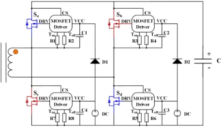
2.2. Controllable Rectifier Circuit
In order to achieve rapid equalization, the equalization current through the transformer’s secondary side becomes very large. Because diode-based rectifiers produce very high heat loss, we decided to replace the diodes with low on-resistance MOSFETs to effectively improve the rectifier efficiency.
In order to satisfy the operation requirements of a supercapacitor equalizing system, we chose MOSFET IRFS7434-7PPBF designed by IR Company. The on-resistance is about 0.7 mΩ with a
maximum value of 1 mΩ. The leakage current is as much as 240 A. Figure5shows a schematic of the
proposed rectifier.
Figure 5.The schematic of the controllable rectifier.
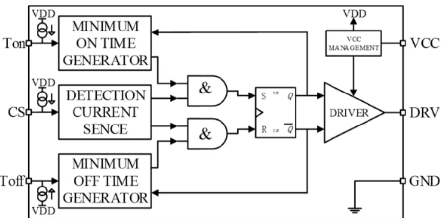
Figure 6.The structure of the MOSFET driver.
2.3. Voltage Equalization Control Algorithm
The proposed equalizing scheme involves transferring energy from the supercapacitor stack to cells with low voltage. Then, the voltages among supercapacitors can be equalized. A controller measures the voltages of cells and computes the maximal voltage difference among supercapacitors. If the lowest voltage isuiand the highest voltage isuj,∆uijrepresents the voltage difference between
thej-th andi-th supercapacitor cell,i.e.,∆uij =uj−ui. When∆uij is larger than a small threshold
u∗
, the corresponding rectifier connected to thei-th supercapacitor cell is enabled, and an equalizing current is supplied to thei-th cell, which transfers energy from other cells to thei-th cell. At the same time, the voltages of other cells decrease because of the energy transfer.
Because the equalization current is very large, the voltage drop for the equivalent resistance of the supercapacitor is large. Then, the terminal voltageui cannot accurately represent the capacitor
voltage when the supercapacitor is charged with the equalization current. In order to avoid this shortcoming, we adopted a pulse equalizing method,i.e., the equalizer only works for a small duration and then stops until the current ripples disappear. The equalizer then measures the voltage of the supercapacitors again and starts the next equalization cycle.
Note that there is noise in the voltage measurements. Thus, it is difficult to ensure that all supercapacitor voltages are completely the same. When all of the supercapacitor voltage differences are within the thresholdu∗
, the voltages are considered to be equalized. The voltage equalization control algorithm is as follows:
Algorithm 1: Voltage equalization control
1: Initialization.
2: Measure the voltages of all supercapacitors.
3: Find the highest voltage celljand lowest voltage celli.
4: Calculated the voltage difference betweenuianduj:∆uij=uj−ui.
5: If∆uij>u∗, then
6: Enable thei-th rectifier.
7: Enable the remaining rectifier for a short time. 8: Disable thei-th rectifier.
9: End if. 10: Go to step 2. 11: End.
3. Implementation and Experimental Results
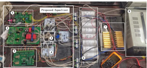
eight controlled rectifiers, a current measure board, a supercapacitor stack, a discharge load and a current charger. Figure7b shows the controlled rectifier, which is the fourth part in Figure7a. Figure7c shows the control board, which is the first part in Figure7a.
(a)
(b) (c)
Figure 7. The experiment setup. (a) Voltage equalizer test bench; (b) controlled rectifier; (c) control board.
As shown in Figure7a, the hardware components of the proposed equalizer were divided into five parts: control board, push-pull forward converter, multi-winding transformer, controlled rectifiers and current measure board. The control board measured the terminal voltage of each supercapacitor cell and regulated the equalization circuit based on these measurements. The current measure board was used to measure and record the equalization current. The supercapacitor stack was connected with the equalizer and could be charged by the current charger and discharged through the discharge load, which was used to imitate the charging and discharging process of renewable energy storage systems. In what follows, we will introduce these components in detail.
Supercapacitor stack: The supercapacitor stack consisted of eight series supercapacitors. Each supercapacitor had a rated voltage of 2.7 V and a rated capacity of 3000 F.
forward converter→transformer→rectifier→supercapacitor cell. In the experiment, the duty cycles of switchesS1andS2were 0.5,i.e., the two switches were turned on alternately.
Multi-winding transformer: The multi-winding transformer was mainly used for the energy transfer and used to maintain electrical isolation among rectifiers. The multi-winding transformer had two primary windings and eight secondary windings. The primary winding was connected to the push-pull forward converter. Each secondary winding was connected to a rectifier circuit. A toroidal core was used to simplify the transformer outgoing line design.
Controlled rectifier: As shown in Figure 7b, controlled rectifiers were used to convert the alternating current to a direct current. There were eight controlled rectifiers in the voltage equalizer. Each rectifier connected one secondary winding of the transformer and one supercapacitor cell. The rectifier circuit could reach dozens of amperes and even hundreds of amperes. In order to ensure a good cooling effect and increase system reliability, the rectifier circuit was formed on the base of a double-sided aluminum substrate.
The MOSFET driver was used to control the switching on or switching off of MOSFETs of the rectifier. The control port of the control board was connected to the control port of the rectifier. The control board could enable or disable the rectifier with a control signal through the control ports. The control board determined if the rectifier needed to be enabled. When the rectifier was enabled, the energy flowed into the corresponding supercapacitor.
Control board: As shown in Figure7c, the control board was the core of the voltage equalizer. The control board was used to measure all supercapacitor voltages and to control the rectifiers. The control board consisted of a voltage measurement module, controller, communication module, CAN module and control port. The voltage measurement module used a high-precision voltage sampling chip to measure all supercapacitor voltages. A LPC1768 microcontroller was used as the controller to run the algorithm. The communication module was used to communicate with the computer. All supercapacitor voltage data were transmitted to the PC. The CAN module was mainly used for inter-module communication and data exchange between primary and secondary equalizers. In the experiment, the CAN module worked as the communication interface between the control board and current measure board. The control ports were connected to the rectifier boards. The control board determined which rectifier needed to be enabled based on the result of the control algorithm.
Current measure board: The current measure board was used to measure the equalization currents. There is a current sensor between each rectifier and the corresponding supercapacitor cell. The current measure board transmitted the sensor data to the control board through CAN module.
Current charger: The current charger was used to charge the supercapacitors. The charging process of supercapacitors with renewable energy sources, such as solar and wind energy, can be simulated by controlling the output current of the charger.
Discharge load:The discharge load was the load of the supercapacitors and was used to emulate the discharge process of supercapacitors. The discharge load was a 1.6Ωresistor connected with the
supercapacitor stack in parallel. The supercapacitor stack could discharge through the resistor load, which could emulate the discharging process.
Figure8shows the switching transitions of switchesS1,S1aandS1bwhen the controller enabled
the first rectifier.Vgs1is the gate-source voltage of switchS1, andVgs1aandVgs1bare the gate-source
voltages of switchesS1aandS1b. WhenS1was on (Vgs1was 15 V), the rectifier ensured thatS1a(S1d)
was on andS1b(S1c) was off. Otherwise, whenS2was on,i.e.,S1was off,S1b(S1c) was on andS1a(S1d)
Figure 8.Switching transitions of switchesS1,S1aandS1b.
Figure9shows the secondary side current of the transformer.Vgs2is the gate-source voltage of switchS2. Isecis the measured secondary side current of the transformer. BecauseS1andS2were turned on alternately, the durations of Mode 3 (t2-t3) and Mode 6 (t5-t6) were approximately zero. Based on the theoretical analysis in Section2, whenS2was off andS1was on, the leakage current of the primary side was fed back to the supercapacitor stack and clamping capacitor. The secondary side current rapidly decreased to zero. Fromt1, the supercapacitor stack and clamping capacitor supplied energy to the secondary side, and the secondary side current increased.S1was off, andS2was on at t2; the secondary side current rapidly decreased to zero and then increased. Thus, the experimental results conformed well to the theoretical analysis.
Figure 9.The current through secondary side of the transformer in equalization.
Figure10shows the equalization current from the equalization circuit to the supercapacitor cell during the equalization process.Vgs1is the gate-source voltage of the switchS1.Ieqis the measured
Figure 10.The equalization current supplied to the supercapacitor cell in the equalization process.
The performance of the proposed voltage equalizer is evaluated under three different operating conditions.
• Case I. All supercapacitor cells have different initial voltage values and are charged with a 10-A
constant current source.
• Case II. All supercapacitor cells have different initial voltage values and discharge through
connecting a 1.6Ωresistor in parallel.
• Case III. All cells have different initial voltage values without charging and discharging.
The initial voltage of supercapacitor cells in different operating conditions is shown in the Table1.
Table 1.The initial voltage of supercapacitor cells.
The Voltage of Cells Case I Case II Case III
VC1 1.693 V 1.749 V 1.814 V VC2 1.677 V 1.762 V 1.810 V VC3 1.682 V 1.761 V 1.820 V VC4 1.602 V 1.698 V 1.658 V VC5 1.702 V 1.766 V 1.833 V VC6 1.672 V 1.783 V 1.815 V VC7 1.673 V 1.742 V 1.767 V VC8 1.517 V 1.639 V 1.606 V Maximum Difference 0.185 V 0.144 V 0.227 V
cell voltages differed owing to the individual cell capacities. When the voltage difference was larger than 20 mV, the equalizer worked to equalize the cell voltages. When the charging process was over, the maximum voltage difference was 20 mV.
The equivalent circuit of the supercapacitors contained an internal resistance. When the equalizer worked, the equalizing current was large, the resistor voltage was large and the terminal voltage could no longer be treated as the cell voltage. Figure11b shows the equalization currentieq of each cell.
The equalization current ofC8could be as high as 54 A, which resulted in an abrupt terminal voltage increase. Though the practical voltage ofC8was the lowest, the terminal voltage ofC8was the highest. In the experiment, a pulse equalizing scheme was applied to mitigate the internal resistance effect.
(a)
(b)
In order to emulate the discharging process of supercapacitor modules, supercapacitors were discharged with parallel resistors. Figure12a shows the voltage curve during discharge. The initial voltage difference was 144 mV. Similar to the charging process, the voltage of the cell with the lowest voltage increased rapidly, and the voltages of the other cells decreased rapidly until equalization was achieved. Figure12b shows the equalization current of cells during the discharging process.
(a)
(b)
Figure 12. The voltage discharging process. (a) The cell voltage profiles; (b) the equalization current profiles.
The initial voltage difference was set to 227 mV. After about 40 s, all cells’ voltages reached equilibrium. The maximal voltage difference was 19 mV after equalization. Figure13a presents the voltage curves of supercapacitor cells, and Figure13b presents the equalization current through supercapacitor cells during equalization. From Figure13b, it can be seen that the maximal equalization current could reach to 60 A. With the equalization process, the cell voltage increased and the equalization current decreased gradually. Because there exist differences in the equivalent inter-resistances and equivalent resistances among different supercapacitor cells and different rectifiers, the equalization currents were different. More total resistance leads to less output equalization current.
(a)
(b)
The efficiency of the equalization circuit could be obtained by calculating the ratio of output power and input power. For convenience, the 15-V constant voltage power supply was adapted to replace the supercapacitor stack as the input of the equalization system. At the same time, the rectifier circuit can be controlled to ensure only one supercapacitor cell participated in the voltage equalization operation during the steady state. Figure14presents the transfer efficiency under different equalization currents, which are obtained from a practical test.
Figure 14.The transfer efficiency under different equalization currents.
From Figure14, it is seen that the highest transfer efficiency of the proposed equalization scheme approaches 92%. With the increase of equalizing current, the system efficiency decreased. When the output current is 41 A, the system efficiency is 83%. The reason is that when output current increased, the energy loss of the secondary rectifier circuit was proportional to the square of the current.
As traditional rectifier diodes work with 0.7 V or a higher forward voltage drop, the conduction power loss of a single diode will reach 28 W when the equalization current is 40 A. This energy loss is unacceptable. In this paper, traditional diodes are replaced with MOSFET IRFS7434-7PPBF. The breakover resistance is about 0.7 mΩwith a maximum value of 1 mΩ. Therefore, the conduction
power loss of a single MOSFET will be less than 1.6 W when the equalization current reaches 40 A. The power loss of the secondary side rectifier circuit is greatly reduced. In addition, there is a certain equivalent resistance between the rectifier circuit and each supercapacitor cell.
When the system is deployed in the experiment, the MOSFETs with low breakover resistance should be selected for secondary side rectifier circuit. Additionally, the wires between rectifier circuit and supercapacitors need to be shortened as much as possible to reduce the energy loss on output wires.
4. Conclusions
accurately equalize the voltages of the supercapacitors, a simple pulse equalizing method is proposed. The experimental results verified the high efficiency of the proposed equalizing scheme.
Acknowledgments: This work was partially supported by the National Nature Science Foundation (Grant Nos. 61202342, 61379111, 61402538, 61403424, 61502055).
Author Contributions: The voltage equalization circuit schematic was proposed by Zhiwu Huang. The experiment results were collected and analyzed by Liran Li and Honghai Lu. The paper was written by Liran Li and Heng Li.
Conflicts of Interest:The authors declare no conflict of interest.
References
1. Baek, S.; Park, E.; Kim, M.G.; Kwon, S.J.; Kim, K.J.; Ohm, J.Y.; Del Pobil, A.P. Optimal renewable power generation systems for Busan metropolitan city in South Korea. Renew. Energy2016,88, 517–525.
2. Benyahia, N.; Denoun, H.; Zaouia, M.; Tamalouzt, S.; Bouheraoua, M.; Benamrouche, N.; Rekioua, T.; Haddad, S. Characterization and control of supercapacitors bank for stand-alone photovoltaic energy.
Energy Proced.2013,42, 539–548.
3. Mahlia, T.; Saktisahdan, T.J.; Jannifar, A.; Hasan, M.H.; Matseelar, H. A review of available methods and development on energy storage; technology update. Renew. Sustain. Energy Rev.2014,33, 532–545. 4. Vazquez, S.; Lukic, S.M.; Galvan, E.; Franquelo, L.G.; Carrasco, J.M. Energy storage systems for transport
and grid applications. IEEE Trans. Ind. Electron.2010,57, 3881–3895.
5. Worku, M.Y.; Abido, M.A.; Iravani, R. Power fluctuation minimization in grid connected photovoltaic using supercapacitor energy storage system. J. Renew. Sustain. Energy2016,8, 013501.
6. Tani, A.; Camara, M.B.; Dakyo, B. Energy Management in the Decentralized Generation Systems Based on Renewable Energy—Ultracapacitors and Battery to Compensate the Wind/Load Power Fluctuations.
IEEE Trans. Ind. Appl.2015,51, 1817–1827.
7. Khare, V.; Nema, S.; Baredar, P. Solar–wind hybrid renewable energy system: A review. Renew. Sustain. Energy Rev.2016,58, 23–33.
8. Rodrigues, E.; Godina, R.; Santos, S.F.; Bizuayehu, A.W.; Contreras, J.; Catalão, J. Energy storage systems supporting increased penetration of renewables in islanded systems. Energy2014,75, 265–280.
9. Kim, S.H.; Choi, W.; Lee, K.B.; Choi, S. Advanced dynamic simulation of supercapacitors considering parameter variation and self-discharge.IEEE Trans. Power Electron.2011,26, 3377–3385.
10. Gualous, H.; Louahlia, H.; Gallay, R. Supercapacitor characterization and thermal modelling with reversible and irreversible heat effect. IEEE Trans. Power Electron.2011,26, 3402–3409.
11. Díaz-González, F.; Sumper, A.; Gomis-Bellmunt, O.; Villafáfila-Robles, R. A review of energy storage technologies for wind power applications.Renew. Sustain. Energy Rev.2012,16, 2154–2171.
12. Lambert, S.; Pickert, V.; Holden, J.; Li, W.; He, X. Overview of supercapacitor voltage equalisation circuits for an electric vehicle charging application. In Proceedings of the 2010 IEEE Vehicle Power and Propulsion Conference, Lille, France, 1–3 September 2010; pp. 1–7.
13. Hua, C.C.; Fang, Y.H.; Li, P.H. Charge equalisation for series-connected LiFePO4 battery strings.
IEEE Trans. Power Electron.2015,8, 1017–1025.
14. Park, H.S.; Kim, C.H.; Park, K.B.; Moon, G.W.; Lee, J.H. Design of a charge equalizer based on battery modularization.IEEE Trans. Veh. Technol.2009,58, 3216–3223.
15. Kim, J.; Shin, J.; Chun, C.; Cho, B.H. Stable configuration of a Li-ion series battery pack based on a screening process for improved voltage/SOC balancing.IEEE Trans. Power Electron.2012,27, 411–424.
16. Uno, M.; Tanaka, K. Accelerated charge-discharge cycling test and cycle life prediction model for supercapacitors in alternative battery applications.IEEE Trans. Ind. Electron.2012,59, 4704–4712.
17. Lisbona, D.; Snee, T. A review of hazards associated with primary lithium and lithium-ion batteries.
Process Saf. Environ. Prot.2011,89, 434–442.
18. Raman, S.R.; Xue, X.D.; Cheng, K. Review of charge equalization schemes for Li-ion battery and super-capacitor energy storage systems. In Proceedings of the 2014 International Conference on Advances in Electronics, Computers and Communications (ICAECC), Bangalore, India, 10–11 October 2014; pp. 1–6. 19. Rahimi-Eichi, H.; Ojha, U.; Baronti, F.; Chow, M. Battery management system: An overview of its application
20. Thounthong, P.; Chunkag, V.; Sethakul, P.; Sikkabut, S.; Pierfederici, S.; Davat, B. Energy management of fuel cell/solar cell/supercapacitor hybrid power source. J. Power Sourc.2011,196, 313–324.
21. Pegueroles-Queralt, J.; Bianchi, F.D.; Gomis-Bellmunt, O. A Power Smoothing System Based on Supercapacitors for Renewable Distributed Generation. IEEE Trans. Ind. Electron.2015,62, 343–350. 22. Gee, A.M.; Robinson, F.V.P.; Dunn, R.W. Analysis of Battery Lifetime Extension in a Small-Scale Wind-Energy
System Using Supercapacitors. IEEE Trans. Energy Convers.2013,28, 24–33.
23. Kollimalla, S.K.; Mishra, M.K.; Narasamma, N.L. Design and Analysis of Novel Control Strategy for Battery and Supercapacitor Storage System. IEEE Trans. Sustain. Energy2014,5, 1137–1144.
24. Thounthong, P.; Luksanasakul, A.; Koseeyaporn, P.; Davat, B. Intelligent Model-Based Control of a Standalone Photovoltaic/Fuel Cell Power Plant With Supercapacitor Energy Storage. IEEE Trans. Sustain. Energy2013,4, 240–249.
25. Beardsall, J.C.; Gould, C.A.; Al-Tai, M. Energy storage systems: A review of the technology and its application in power systems. In Proceedings of the 2015 50th International Universities, Power Engineering Conference (UPEC), Stoke-on-Trent, UK, 1–4 September 2015; pp. 1–6.
26. Kim, C.H.; Kim, M.Y.; Park, H.S.; Moon, G.W. A modularized two-stage charge equalizer with cell selection switches for series-connected lithium-ion battery string in an HEV. IEEE Trans. Power Electron. 2012,
27, 3764–3774.
27. Ma, T.; Yang, H.; Lu, L. Development of hybrid battery–supercapacitor energy storage for remote area renewable energy systems.Appl. Energy2015,153, 56–62.
28. Phung, T.H.; Crebier, J.C.; Lembeye, Y. Voltage balancing converter network for series-connected battery stack. In Proceedings of the IECON 2012–38th Annual Conference on IEEE Industrial Electronics Society, Montreal, QC, Canada, 25–28 October 2012; pp. 3007–3013.
29. Thanh, H.P.; Collet, A.; Crebier, J.C. An Optimized Topology for Next-to-Next Balancing of Series-Connected Lithium-ion Cells. IEEE Trans. Power Electron.2014,29, 4603–4613.
30. Uno, M.; Kukita, A. Single-Switch Single-Transformer Cell Voltage Equalizer Based on Forward-Flyback Resonant Inverter and Voltage Multiplier for Series-Connected Energy Storage Cells.IEEE Trans. Veh. Technol.
2014,63, 4232–4247.
31. Lim, C.S.; Lee, K.J.; Ku, N.J.; Hyun, D.S.; Kim, R.Y. A modularized equalization method based on magnetizing energy for a series-connected lithium-ion battery string. IEEE Trans. Power Electron.2014,29, 1791–1799.
c