A Non-Scan DFT Method at Register-Transfer Level
to Achieve Complete Fault Efficiency
Satoshi Ohtake, Hiroki Wada, Toshimitsu Masuzawa and Hideo Fujiwara Graduate School of Information Science, Nara Institute of Science and Technology
8916-5, Takayama, Ikoma, Nara 630-0101, Japan
E-mail: ohtake, hiroki-w, masuzawa, fujiwara @is.aist-nara.ac.jp Abstract — This paper presents a non-scan design-for-
testability (DFT) method for VLSIs designed at register- transfer level (RTL) to achieve complete fault efficiency. In RTL design, a VLSI generally consists of a controller and a data path. The controller and the data path are con- nected with internal signals: control signals and status sig- nals. The proposed method consists of the following two steps. First, we apply our DFT methods [1] and [2, 3] to the controller and the data path, respectively. Then, to support at-speed testing, we append a test plan generator which generates a sequence of test control vectors for the modified data path. Our experimental results show that the proposed method can reduce significantly both of test generation time and test application time compared with the full-scan design, though the hardware overhead of our method is slightly larger than that of the full-scan design.
I. INTRODUCTION
With the advance in semiconductor technology, the com- plexity of VLSI designs is growing and the cost of testing is increasing. Therefore, it is necessary to reduce cost of testing and to enhance quality of testing. The cost of testing is esti- mated by test generation time and test application time. The quality of testing is estimated by fault efficiency1. Therefore, we have to reduce test generation time and test application time and to enhance fault efficiency. To ease the complexity of test generation, design-for-testability (DFT) techniques have been proposed. The most commonly used DFT techniques for se- quential circuits are scan-based approaches[4]. These tech- niques modify sequential circuits so that automatic test pat- tern generation (ATPG) tools can achieve high fault efficiency in a reasonable time. However, these techniques sacrifice the possibility of at-speed testing[5] for fault efficiency enhance- ment. To avoid this disadvantage of scan techniques, several non-scan approaches have been investigated. Moreover, since techniques of test generation and DFT at gate level face the problems arising out of huge number of elements and high complexities of the circuits at gate level, several techniques of test generation and DFT at register-transfer level (RTL) have been proposed recently.
In RTL design, a VLSI circuit is generally described by a controller part and a data path part separately. The former is represented by a state transition graph (STG) and the latter is represented by hardware elements (e.g. registers, multiplexers and operational modules) and lines. A controller and a data
1Fault efficiency is the ratio of the number of faults detected and proved redundant to the total number of faults.
path are connected with internal signals: control signals and status signals. Most of the DFT methods for RTL circuits were concerned with only either data paths or controllers, un- der assumption that the control signals and the status signals are directly controllable and observable from the outside of the VLSI.
For controllers, Chakradhar et al.[6] proposed a non-scan DFT method at RTL. This method can achieve high fault ef- ficiency but cannot always guarantee complete (100%) fault efficiency. Furthermore, it is applicable only to PLA-based se- quential circuits. Our previous work [1, 7] proposed several non-scan DFT methods which achieve 100% fault efficiency. In these methods, given an STG, we first synthesize a sequen- tial circuit from the STG. Then we generate test patterns, by a combinational ATPG tool, for the combinational part of the synthesized sequential circuit. Most of the generated test pat- terns can be applied to the sequential circuit using state transi- tions of the STG. However, there may exist test patterns which cannot be applied using state transitions of the STG. In this case, we append an extra logic which provides extra transi- tions required for testing. Those test patterns are applied using the extra logic.
For data paths, several non-scan DFT methods at RTL have been reported, e.g. orthogonal scan[8, 9] and H-SCAN[10], which use normal data path flow as scan path instead of tra- ditional scan path flow. These methods can reduce hardware overhead and test application time compared with the full-scan design. However, test generation time cannot be reduced be- cause the test generation approach is the same as the full-scan design. To reduce test generation time, a hierarchical test gen- erationapproach was proposed by Murray and Hayes[11]. The hierarchical test generation of a data path consists of the fol- lowing two steps: for individual combinational hardware el- ements, generate test patterns at gate level and generate test plansat RTL, where a test plan is a control sequence to prop- agate test patterns from the primary inputs to the inputs of the respective hardware elements and to propagate responses from the output of the respective hardware elements to the primary outputs. Genesis [12]–[15] is an approach based on such hier- archical test generation for data paths. However, Genesis can- not always guarantee 100% fault efficiency due to the back- tracking in the test plan generation for large data paths. Our previous work [2, 3] presented a DFT method based on such hierarchical test generation and strong testability. Strong testa- bility is a property of data paths which guarantees to generate test plans for all combinational hardware elements of the data path. In our method, test plans can be derived with complexity O n2 where n is the number of hardware elements in a RTL data path.
Asia and South Pacific Design Automation 2000 (ASP-DAC 2000), pp. 599-604, Jan. 2000.
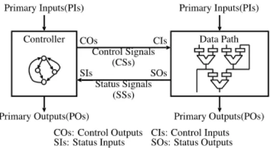
Controller Data Path Control Signals
(CSs) Status Signals
(SSs)
Primary Inputs(PIs)
Primary Outputs(POs) Primary Inputs(PIs)
Primary Outputs(POs)
COs CIs
SIs SOs
CIs: Control Inputs SOs: Status Outputs COs: Control Outputs
SIs: Status Inputs
Fig. 1.An RTL controller/data path circuit.
This paper presents a DFT method for an RTL circuit which consists of a controller part and a data path part. Given an RTL controller/data path circuit, we apply the DFT method of [1] to the controller part and apply that of [2, 3] to the data path part. Our previous experimental results using benchmark circuits show that the hardware overheads of [1] and [2, 3] were 3.5% and 4.0% on average, respectively. The test application times in [1] and [2, 3] were reduced on average to 25.4% and 17.6% of the full-scan design, respectively. Furthermore, both of these DFT methods can achieve 100% fault efficiency and allow at-speed testing.
In the above-mentioned DFT methods, we assumed that both control signals and status signals between a controller and a data path are directly controllable and observable from the outside of circuits. However, if we consider a DFT method for the whole circuit consisting of both a controller and a data path, we have to remove this assumption by adding some extra logic to provide both controllability and observability of those con- trol and status signals. In this paper, we resolve this problem by (1) adding multiplexers on those control and status signals to connect directly from primary inputs and to primary outputs and (2) embedding an extra circuit in the controller side, called a test plan generator, which can generate test plans for the data path of an RTL circuit.
The proposed DFT method for controller/data path circuits has the following advantages:
100% fault efficiency can be achieved. At-speed testing can be performed. Furthermore, from our experimental results,
Test application time can be reduced significantly com- pared with the full-scan design.
Test generation time can be reduced significantly com- pared with the full-scan design.
The hardware overhead is slightly large compared with the full-scan design and the difference between the over- heads is small.
This paper is organized as follows: Section II gives the def- inition of controller/data path circuits. In Section III, we intro- duce the DFT methods of controllers reported in [1] and of data paths reported in [2, 3] and propose a DFT method of whole circuits consisting of both controllers and data paths. Section IV shows experimental results of the proposed method.
II. PRELIMINARIES
In RTL description, a VLSI circuit generally consists of a controller and a data path as shown in Fig. 1. The former is rep- resented by an STG and the latter is represented by hardware elements (e.g. registers, multiplexers and operational modules) and lines. Each of the controller and the data path has primary inputsfrom the outside of the VLSI and primary outputs to the outside of the VLSI. The controller also has status inputs from
the data path and control outputs to the data path. Similarly, the data path also has control inputs from the controller and status outputsto the controller. The signals from the control outputs to the control inputs are called control signals, and the signals from the status outputs to the status inputs are called status signals.
Data Path
A data path consists of hardware elements and lines. A hard- ware element is a primary input, a primary output, a control in- put, a status output, a register, a multiplexor, or an operational module, and a line connects two hardware elements with some bit width. Inputs of a hardware element of a data path can be classified into data inputs and control inputs. Data inputs of a hardware element are connected directly/indirectly from primary inputs of the data path. Control inputs of a hardware element are connected directly from control inputs of the data path. Examples of the control inputs are load enable signals of registers, selection signals of multiplexers and function se- lection signals of operational modules. Similarly, outputs of a hardware element of a data path can be classified into data outputsand status outputs. Data outputs of a hardware element are connected directly/indirectly to primary outputs of the data path. Status outputs of a hardware element are connected di- rectly to status outputs of the data path. An Example of hard- ware elements which have status outputs is a comparator.
III. A METHOD OFDFTFORRTL CONTROLLER/DATA
PATHCIRCUITS
In this section, we propose a DFT method for controller/data path circuits.
A. Overview
In our DFT method, given a controller/data path circuit de- scribed at RTL, we first apply the DFT method of [1] to the controller and apply that of [2, 3] to the data path of the circuit. In these DFT methods, we assume that the control signals and the status signals are directly controllable and observable from the outside of the circuit. However, these are internal signals between the controller and the data path in the controller/data path circuit. Thus, for testing of the controller, we have to en- hance controllability of the status inputs and observability of the control outputs. Similarly, for testing of the data path, we have to enhance controllability of the control inputs and ob- servability of the status outputs. In the DFT method proposed in this paper, we embed mechanisms to enhance controllability and observability of the control signals and the status signals so that the testing method of [1, 2, 3] can be applied. The test architecture of the controller/data path circuit of our method is shown in Fig. 2.
Before explaining the details of the test architecture, we briefly introduce the DFT methods for controllers and data paths that are basis of the test architecture.
B. DFT of Controllers [1]
In this section, we give an overview of the DFT method [1] for a controller synthesized from an STG. The method achieves 100% fault efficiency with short test generation time and al- lows at-speed testing. In order to generate a test sequence that achieves 100% fault efficiency with short test generation time, we generate test patterns for the combinational part of the se- quential circuit using a combinational ATPG tool. Each of test patterns consists of the values corresponding to primary inputs
PIs
POs
PIs
POs TMR
TPR Test Controller
Controller
I SG MUX
Data Path
Hold Mask
TPG
ACSs CSs
SSs
t0 t1
t2 t3
t4
Mask
REG Hold REG Hold
REG
MUX1 MUX2
t out MUX3 Reset
t1
COs
SIs
CIs
SOs ACIs
TP G: Test Plan Generator ACSs: Additional Control Signals TPR: Test Pattern Register
TMR: Target Module Register ACIs: Additional Control Inputs
ti: Test Pin
Fig. 2.Test architecture of a controller/data path circuit. CC
PIs POs
SR
t out t3
t4
R
I SG MUX
1 0 0 1
t3: mode switching signal t out: state output signals t4: load/hold signal I SG: invalid test state genarator
CC: combinational logic block SR: state register
SIs COs
Fig. 3.A controller augmented with an extra logicI SG.
(PIs), status inputs (SIs) and a state register (SR) of the sequen- tial circuit. In order to apply a test pattern to the combinational part, we have to set the corresponding value to the SR. If the value corresponds to a state reachable from the reset state of the STG, the value can be set to the SR using original state transitions of the STG. Otherwise, the value cannot be set to the SR using state transitions of the STG. In order to set such a value to the SR, we append an extra logic called an invalid test state generator(I SG) to the controller as shown in Fig. 3. The I SGgenerates all the values (called invalid test states) that ap- pear in the test patterns but cannot be set to the SR using state transitions of the STG. In Fig. 3, t3is used to select inputs of the SR: the outputs of the original combinational logic block or those of theI SGand t4is a load/hold signal and is utilized to reduce test application time.
The complete fault efficiency is preserved because the com- binational logic block remains unchanged. Our experimental results using benchmark circuits show that the average hard- ware overhead of theI SGis only 3.5%[1] and the average test application time of the method is 25.4% of that of the full-scan design[1].
Notice that, in this method, we assume that the status inputs and the control outputs of the controller are directly control- lable and observable from the outside of the circuit, respec- tively. However, these are internal signals in the controller/data path circuit. Thus, in the DFT proposed in this paper, the con- troller/data path circuit is modified so that the status signals and the control signals can be directly controlled and observed from the outside of the circuit. A straight forward solution is to introduce additional test pins and to connect them directly to the status inputs and the control outputs. However, this solu- tion introduces unacceptable pin overhead for practical design.
TABLE I
CONFIGURATIONS OF TEST ARCHITECTURE Test Pins
t0 t1 t2 t3 t4 Operation 0 0 0 0 0 Normal operation 1 0 1 Testing controller
0 1 Testing data path
: depend on test patterns or test plans
Instead, in proposed DFT, the pin overhead is avoided as fol- lows: the status inputs of the controller are directly controlled from primary inputs of the data path by adding a multiplexer
“MUX1” as Fig. 2, and the control outputs of the controller are directly observed from primary outputs of the data path by adding a multiplexer “MUX3”. This approach is acceptable because it generally conceivable that the status inputs (resp. the control outputs) of the controller have smaller bit-width than the primary inputs (resp. the primary outputs) of the data path, and we need not use function of the data path at testing of the controller. In testing of the controller, these multiplexers
“MUX1” and “MUX3” are configured as shown in TABLE I. C. DFT of Data Paths [2, 3]
In this section, we give an overview of the DFT method of [2, 3] for a data path described at RTL.
Strong Testability
The DFT method is based on hierarchical test generation and strong testability.
Hierarchical test generation is an efficient technique for generating test patterns of very large data paths. In hierar- chical test generation, test generation of each combinational hardware element M proceeds as follows:
Step 1: Extract M from the data path and generate test patterns of M at logic level using a combinational ATPG tool . Step 2: Generate a test plan which is a sequence of control
vectors of control inputs of the data path for propagating the test patterns obtained at the first step from primary in- puts to the data inputs of M and for propagating responses of M from the data outputs of M to primary outputs. The test patterns and the responses are propagated using orig- inal data path flows of the data path.
Strong testabilityis proposed as a characteristic of data paths that guarantees applicability of the hierarchical test genera- tion.
Definition 1: Strong Testability [2, 3]
A data path is strongly testable iff there exists a test plan for each combinational hardware element M that makes it possible to apply any pattern to M and to observe any response of M. A strongly testable data path has the following advantages.
Fast test pattern generation:
Test pattern generation time is short since a combinational ATPG tool can be applied to each combinational hardware element separately.
Fast test plan generation:
Test plan generation time is short since test plans are gen- erated at RTL (not at gate level).
100% fault efficiency:
100% fault efficiency can be achieved for the whole data path, since each hardware element M is a combinational circuit of small size and strong testability guarantees com- plete controllability and complete observability of M.
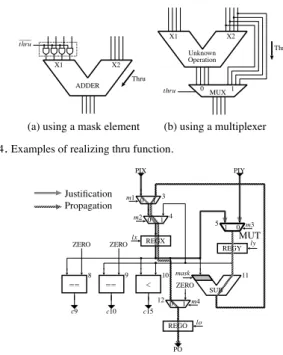
thru
Thru
(a) using a mask element (b) using a multiplexer
thru
Thru
ADDER
X1 X2
Unknown Operation
X1 X2
MUX 1 0
Fig. 4.Examples of realizing thru function.
REGY ly lx REGX
0 1 m2
SUB 0
1 m3
0 1 m4
REGO lo 0 1 m1
PIY
PO PIX
ZERO ZERO
ZERO
c15 c10 c9
mask 3
4 5
8 9 10
12
11 MUT Justification
Propagation
Fig. 5.An example of strongly testable data path.
The DFT Method
In the DFT method, we add no special path for propagating test patterns and responses. Instead, test patterns and responses are propagated along existing data path flows. To propagated test patterns and responses along existing data path flows, the DFT method appends thru functions to operational modules and hold functions to registers. Below we provide a brief ex- planation of the DFT method.
Consider testing of a combinational hardware element M with two data inputs, x and y, in the data path. To test M, a value specified by a test pattern should be fed into x. We prop- agate the value along a path p from a primary input to x. If an operational module C appears on p, the output value of C will depend on the function and the input value(s) of C.
In order to propagate the value of the test pattern along p, thrufunction is added to C. Most of the popular operational modules (e.g. adder) can realize the thru function by using a maskelement. The mask element generates a constant what is required to realize the thru function. Figure 4(a) illustrates an example of such mask element. If we cannot realize the thru function using the mask element, we realize the thru function using a multiplexer as in Fig. 4(b).
However, we cannot achieve the strong testability by adding only the thru functions. The thru functions guarantee controlla- bility of a single path. In case of a hardware element which has two data inputs, a test pattern must be applied to both the inputs simultaneously. Presence of reconvergent paths in a data path can prevent such application of a test pattern to a hardware ele- ment which has two data inputs. In particular, this can happen if the propagation paths to the two data inputs of a hardware element start from the same primary input and have the same sequential depth. Such reconvergent paths will cause a timing conflict, i.e. two different values are required on a primary in- put at the same time. To resolve such conflicts, in the DFT method, some registers are augmented with hold function.
In this DFT, to control the thru functions, and the hold func- tions, additional control inputs are appended as shown in Fig. 2.
Time PIX PIY m1 m2 m3 m4 lx ly lo mask c9 c10 c15 PO
1 C X 0 0 X X 1 X X X - - - - Justification
2 X C X X T X X 1 X X - - - -
3 X X 1 0 X X 1 X X 1 - - - - Propagation
4 X X X X X 0 X X 1 X - - - -
5 X X X X X X X X X X - - - O
C : apply test pattern to PI X : don’t care O : observe PO and/or status output - : need not observe T : apply test pattern to control input
Fig. 6.An example of test plan.
An example of application of the DFT method is shown in Fig. 5. In this example, a mask element is added to an data input of subtracter “SUB” and an additional control input is
“mask”. Time complexities of the DFT algorithm and the test plan generation algorithms are O n and O n2 , respectively, where n is the number of hardware elements in the data path. Our experiments using benchmark circuits show that the aver- age hardware overhead is only 4.0% and the average test ap- plication time is 17.6% of that of the full-scan design[2, 3]. Test Plans
For every combinational hardware element of a data path, a test plan can be generated by the algorithm of [2, 3]. Consider a combinational hardware element M which has data inputs, control inputs, data outputs and status outputs in the data path. Each test pattern of M consists of a value corresponding to the data inputs and a value corresponding to the control inputs. We call the former a data input value and the latter a control input value. Notice that, for testing such a hardware element, we must apply test patterns both the data inputs and the control in- puts. The test plan propagates the data input value to the data inputs of M from primary inputs. The test plan also applies control input value to the control inputs at the time when the data input value is justified to the data inputs. The test plan also propagates the responses appeared on the data outputs of Mfrom the data outputs to the primary outputs. The response appeared on the status outputs of M is observable from status outputs of the data path. For example, a test plan of the multi- plexer marked MUT in Fig. 5 is shown in Fig. 6.
Computation time of the test plan generation algorithm is O n2 where n is the number of hardware elements in the data path, and on experimental results show that the average test application time of the method is 17.6% of that of the full-scan design[2, 3].
Notice that, the test plans and control input values of hard- ware elements must be applied to the control inputs (including control inputs appended by the DFT) of the data path. Simi- larly, the responses on the status outputs of the data path must be observed from the status outputs. If we use additional test pins to make these such control inputs and status outputs di- rectly controllable and observable, respectively, from the out- side of controller/data path circuits, pin overhead is unaccept- able for practical designs. The problem of the pin overhead can be avoided by the following way. Here, we first consider ob- servability of the status outputs. In general, since the bit-width of the primary outputs of the controller is smaller than that of the status outputs, we cannot use the primary output for observ- ing the status outputs. However, the bit-width of the primary outputs of the data path is larger than the status outputs. Since observation of a response of a test pattern only from either the status outputs or the primary inputs is sufficient, the status out- puts and the primary outputs need not observed simultaneously at testing of the data path. Therefore, we can observe the status
outputs using the primary outputs of the data path. In our test architecture, this is achieved by a multiplexer “MUX3” (see Fig. 2).
We next consider controllability of the control inputs. In general, since the number of primary inputs of the controller is smaller than that of control inputs of the data path, we cannot use the primary inputs for applying test plans and control input values of hardware elements to the control inputs. Moreover, in testing of data path, since the primary inputs of the data path are used to apply data input values of hardware elements, we cannot use them to apply the test plans and the control input values to the control inputs of the data path simultaneously. Therefore, we append an extra circuit called a test controller to generate control input values as shown in Fig. 2. The detail of the test controller is presented in the next subsection.
D. Test Plan Generator
Test plans are generated for the all combinational hardware elements in a data path of a controller/data path circuit. In our test architecture, all the test plans of the data path are generated by a test controller (Fig. 2). The test controller consists of a test plan generator(TP G), a test pattern register(TPR) and a target module register(TMR) as shown in Fig. 2. Consider testing of a combinational hardware element M, which has data inputs and control inputs, in the data path. The TMR is used to store the index of M. The bit width of the TMR is log m where m is the number of combinational hardware elements in the data path. TheTP G generates the test plan of M from the index stored in the TMR. When the a data input value of a test pattern of M is justified to the data inputs, if some primary inputs of the data path are not used, the control input value is applied from such primary inputs by way ofTP G. Otherwise, the control input value is pre-stored in the TPR and is applied to the control inputs by way ofTP G. The load enable signal for TPR and TMR is directly connected from the reset signal of the controller. That is, if reset is applied, TPR and TMR load values from some primary inputs of the data path, otherwise, they hold their values. The mode switching signal t1 is used to disable DFT elements of the data path in normal operation mode.
In testing of the data path, the advantage of using theTP G is that test patterns of each combinational hardware element of the data path can be applied to the combinational hardware element at operational speed of the circuit because we can run theTP G using the system clock of the circuit. Notice that, it is conceivable that the largest delay of paths in theTP Gis much less than that of the critical path in the data path.
We estimate hardware overhead of aTP G of a controller /data path circuit. From our experiments, the area of theTP G is almost the same as the area of the original controller of the circuit. For controller/data path circuits dominated data flow, it is conceivable that hardware overhead of theTP Gis low.
We also consider testing of aTP G. Since theTP G is not used at the normal operation, we test theTP Gonly to confirm that the test plans are generated correctly. It is performed by observing primary outputs of a data path (see Fig. 2).
IV. EXPERIMENTALRESULTS
In this section, we evaluate effectiveness of our method by experiments. Circuit characteristics of RTL benchmark cir- cuits used in the experiments is shown in TABLE II. The cir- cuits GCD, JWF, LWF and PAULIN are popularly used exam- ples and the circuit RISC is a more practical and large proces- sor designed by a semiconductor company. In our experiments,
we used a logic synthesis tool AutoLogicII (MentorGraphics) with its sample libraries to synthesize these benchmark cir- cuits. In this table, column “Area” denotes the total areas after synthesis. Here, areas are estimated using gate equivalent of the library cell area. Columns “Controller” and “Data path” de- note the characteristics of controller parts and data path parts, respectively: columns “#PI”, “#PO” and “Area” denote the numbers of primary inputs and primary outputs and circuit area of respective parts. Columns “#State”, “#Status” and “#Con- trol” in “Controller” denote the numbers of states, of status inputs and of control outputs. Columns “ bit ”, “#Reg.” and
“#Mod.” in “Data path” denote the bit width of data paths and the numbers of registers and of operational modules in data paths. In the row “RISC”, the number of the status signals is larger than that of the primary inputs of the data path. In our DFT, twenty-two primary output pins are changed to primary input/output pins by appending tri-state buffers. However, the hardware overhead of this modification.
Test generation results are shown in TABLE III. Sequen- tial/combinational ATPG tool TestGen (Synopsys) is used in this experiments on Ultra60 model 2360 (SunMicrosystems). Columns “Test generation time”, “Test application time” and
“Fault efficiency” denote test generation time in second, test application time in clock cycles and fault efficiency. In each of these columns, columns “Original”, “Full-scan” and “Our method” denote the results of the original circuits (without DFT), of the circuits modified by full-scan design and of cir- cuits modified by our method. Test generation time of our method is shorter than that of the full-scan design except LWF. Especially, for the circuit RISC, our method can reduce to 1/700 of the full-scan design and can enhance fault efficiency compared with the full-scan design. For the circuit, fault ef- ficiency is 99.99% because the combinational ATPG tool can not generate a test pattern for a fault in a multiplier of the cir- cuit. Test application time of our method is drastically reduced compared with that of the full-scan design.
The area and pin overheads of the full-scan design and our method are shown in TABLE IV. In this results, for all circuits except PAULIN, the area overhead of our method is larger than that of the full-scan design but the difference between the hard- ware overhead of our method and that of the full-scan design is not large. The pin overhead of our method is larger than that of the full-scan design. In the result of the circuit RISC of our method, the pin overhead is larger than the other because two select signals of concatenation of two multiplexers are needed on the primary outputs of the data path to observe the control signals and the status signals from the primary outputs. In re- turn for this disadvantage, our method allows at-speed testing. In our method, hardware for thru and hold functions and multiplexers are appended to a controller/data path circuit. First consider performance degradation of the circuit caused by these appended multiplexers. Multiplexers are appended in front of the state register of the controller in the circuit, on control signals between the controller and the data path in the circuit and in front of the primary outputs of the data path. The multiplexer in front of the state register is the same as the full-scan design. The multiplexer on the control signals does not affect performance of the circuit because the control sig- nals are not generally included in the critical path of the circuit [13]. The multiplexer in front of the primary outputs of the data path does not also affect performance of the circuit be- cause, in general, there exist registers in front of the primary outputs of the data path and delay of multiplexers are less than operational modules.
For the data path, the performance might be degraded by
TABLE II CIRCUIT CHARACTERISTICS.
Controller Data path
Circuit Area(gate) #PI #PO #State #Status #Control Area(gate) #PI #PO bit #Reg. #Mod. Area(gate)
GCD 1524.50 0 1 4 3 7 169.40 32 16 16 3 1 1350.90
JWF 6875.40 0 0 8 0 38 199.50 80 80 16 14 3 6671.70
LWF 1986.20 0 0 4 0 8 57.70 32 32 16 5 3 1924.30
PAULIN 24965.60 0 0 6 0 16 123.50 64 64 32 7 4 24833.70
RISC 62287.60 0 2 11 54 62 3986.90 32 96 32 40 4 58157.90
TABLE III TEST GENERATION RESULTS.
Test generation time(sec.) Test application time(cyc.) Fault efficiency(%) Circuit Original Full-scan Our method Original Full-scan Our method Original Full-scan Our method
GCD 18055.53 171.51 0.69 9 6629 504 4.92 100.00 100.00
JWF 2348.24 2.88 0.98 488 20519 1497 98.14 100.00 100.00
LWF 171.68 0.47 0.81 322 4066 517 99.64 100.00 100.00
PAULIN 20362.55 4.68 2.11 283 16187 2193 97.01 100.00 100.00
RISC 288102.05 51740.92 72.55 4298 1006154 9674 62.31 99.97 99.99
TABLE IV HARDWARE OVERHEADS.
Area overhead(%) Pin overhead(#) Circuit Full-scan Our method Full-scan Our method
GCD 26.6 39.7 3 5
JWF 26.7 28.4 3 5
LWF 33.4 42.3 3 5
PAULIN 7.4 6.3 3 5
RISC 16.7 21.4 3 6
appended hardware for thru and hold functions. In the full- scan design, multiplexers are added to all registers to make each register a scannable register. On the other hand, in our method, thru and hold functions are added to some (not all) operational modules and registers, respectively. Furthermore, delays of hardware for thru and hold functions are less than that of multiplexers. Therefore, performance degradation of our method is smaller than that of full-scan design.
V. CONCLUSION
This paper presented a novel non-scan DFT method for controller/data path circuits designed at RTL. The proposed method can achieve 100% fault efficiency and allows at-speed testing. The hardware overhead of the proposed method is slightly larger than that of the full-scan design but the differ- ence between the overheads is small. In return for the small increase of hardware overhead, since the hierarchical test gen- eration can be applied to the data path part of the circuits, test generation time of the proposed method is shorter than that of the full-scan design. Furthermore, since the proposed method uses no traditional scan path, test application time is very low. Our future work is to reduce hardware overhead of test con- trollers.
ACKNOWLEDGMENTS
This work was supported in part by Semiconductor Technol- ogy Academic Research Center (STARC) under the Research Project. Authors would like to thank Tomoo Inoue of Hi- roshima City University and Michiko Inoue of Nara Institute of Science and Technology for their valuable discussions.
REFERENCES
[1] S. Ohtake, T. Masuzawa and H. Fujiwara: “A non-scan DFT method for controllers to achieve complete fault efficiency,” in Proc. of the 7th Asian test symposium, pp. 204–211, 1998.
[2] T. Masuzawa, H. Wada, K. K. Saluja and H. Fujiwara: “A non-scan DFT method for RTL data paths to achieve complete fault efficiency,” Technical report, Information Science Technical Report: TR98009, Nara Institute of Science and Technology, 1998.
[3] H. Wada, T. Masuzawa, K. K. Saluja and H. Fujiwara: A DFT method for RTL data paths achieving 100% fault efficiency under hierarchical test environment, European Test Workshop, 1999.
[4] H. Fujiwara: Logic Testing and Design for Testability, The MIT Press, 1985.
[5] P. C. Maxwell, R. C. Aitken, V. Johansen and I. Chiang: “The effect of different test sets on quality level prediction: when is 80% better than 90%?,” in Proc. of International Test Conference, pp. 358–364, 1991. [6] S. T. Chakradhar, S. Kanjilal and V. D. Agrawal: “Finite state machine
synthesis with fault tolerant test function,” Journal of Electronic Testing: Theory and Applications, Vol. 4, pp. 57–69, February 1993.
[7] D. K. Das, S. Ohtake and H. Fujiwara: “New DFT techniques of non- scan sequential circuits with complete fault efficiency,” in Proc. of the 8th Asian test symposium, 1999 (to appear).
[8] R. B. Norwood and E. J. McCluskey: “Orthogonal scan: Low overhead scan for data paths,” in Proc. of Int. Test Conf., pp. 659–668, 1996. [9] R. B. Norwood and E. J. McCluskey: “High-level synthesis for orthogo-
nal scan,” in Proc. of 15th VLSI Test Symp., pp. 370–375, 1997. [10] S. Battacharya and S. Day: “H-SCAN: A high-level alternative to full-
scan testing with reduced area and test application time,” in Proc. of the IEEE VLSI Symp., pp. 74–80, 1996.
[11] B. T. Murray and J. H. Hayes: “Hierarchical test generation using pre computed tests for modules,” IEEE Trans. on CAD, Vol. 9, No. 6, pp. 594–603, June 1990.
[12] S. Bhatia and N. K. Jha: “Genesis: A behavioral synthesis system for hierarchical testability,” in Proc. of European design and test conference, pp. 272–276, 1994.
[13] I. Ghosh, A. Raghunath and N. K. Jha: “Design for hierarchical testabil- ity of RTL circuits obtained by behavioral synthesis,” in Proc. of IEEE Int. Conf. on Computer Design, pp. 173–179, 1995.
[14] I. Ghosh, A. Raghunath and N. K. Jha: “A design for testability tech- nique for RTL circuits using control/data flow extraction,” in Proc. of IEEE/ACM Int. Conf. on CAD, pp. 329–336, 1996.
[15] I. Ghosh, A. Raghunath and N. K. Jha: “Hierarchical test generation and design for testability methods for ASPP’s and ASIP’s,” IEEE Trans. on CAD, Vol. 18, No. 3, pp. 357–370, March 1999.