difficult to relate all these aspects by a compactformulawhichcanbe utilized as a performance
metric.
A weakeffort in this respect wasoriginally
done by Mead and Rem [19],[16]
relating the area (A) andthe
speed (T-1) and proposing the rental time of the chip A T as a metric. Thompson [8] has extended the concept for any arbitrary network byshowing that A T2indicates
a betterperformancemetric. He has relatedthe
area and the speed of computation in a network through its minimalbipartition
width, w and have shown that a computational problem can be solvedby
exchanging information overw such that the speed of computation is directly proportional to the cardinality of w while the area of planar implementation of the network is directly proportional to the square of the size ofc.But this metric accounts for the lower bound of thechiparea. Savage [20] has contended that A
2T
reflects a better evaluation forcertain computa- tional problems likebinary
sorting. From all these contradictory claims, it is evident that it is virtually not possible to correlate all the criteria discussed here. An alternative strategy has been adopted here. The networks have been given credit points for each criterion depending on their relative merits and the total points have been used as a performance index for the network. The results of the evaluation with respect to different criteria have been shown in Table I. The credit points have been assigned on the basis of relative merits of the networks.From
the values of total points, it can be seen that the two- dimensional mesh networks indicate overall better performance than the H tree and the CCC. This is in direct contrast to the results of Wittie [3], Siegel [21], [22], etc., who have concluded that fast networks likeCCC,
PSN, spanning bus hypercubes, etc., have better overall performance. It may be argued whether it is appropriate to give same weight to all the criteria. But it can be easily seen that the conclusion remains true even if different weights are ascribed to three orthogonal aspects (i.e., criteriahaving same aspect only have same weight).IV. CONCLUSION
The basic conclusionemerging out of the analyses done here is that thecellular networks which have a similar structure to the mesh can be
cost
effectively implemented for VLSI implementation and are highly suitable for VLSI parallel processing. Thepenalty in delay can be offset by the gains ofseveral criteriadiscussed in this correspon- dence. The faster topologies like CCC, PSN, tree, etc., do not provide an overall good performance because of long interconnects whichintroduce
high delay and large chip area which reduces the chip yield. The conclusion is made here on the basis of the topological properties of the networks and not on actual implementation of a specific algorithm. Special algorithmic features can be exploited to improve the average message delay over aspecific networktopology.ACKNOWLEDGMENT
The author wishes to thank Profs. J. Patel, D. Reed, and B. Wah for their comments on the initial version of this correspondence.
REFERENCES
[1] K. J. Thurber, "Interconnection networks-A survey and assessment," AFIPS Conf. Proc., vol. 43, pp. 909-919, 1974.
[2] G. A. Andersen and E. D. Jensen, "Computer interconnection structures: Taxonomy, characteristicsandexamples," ACM Comput. Survey, vol. 7, pp. 197-213, Dec. 1975.
[3] L. D. Wittie,
."Communications
structures for large networks of microcomputers," IEEE Trans.Comput.,
vol. C-30, pp. 264-273, Apr. 1981.[4] T.-Y. Feng, "A survey of interconnection networks," IEEE Com- puter, vol. 14, pp. 12-27, Dec. 1981.
[5] D. F. Barbe, Very LargeStale Integration: Fundamentals and Applications. Berlin: Springer-Verlag, 1980.
[6] M. J. Atallah, "Algorithms for VLSI networks ofprocessors,' Ph.D. dissertation, Johns HopkinsUniv., Baltimore,MD, 1983.
[7] F. P. Preparata and J. Vuillemin, "The cube connected cycles: A versatile network for parallel
computation,"
in Proc. 20thAnn.IEEE Symp. Foundations Comput. Sci., pp. 140-147, 1979.[8] C. D. Thompson, "Acomplexity theory forVLSI," Ph.D. disserta- tion, Carnegie-Mellon Univ., Pittsburgh, PA, 1980.
[9] C. H. Stapper, "Modeling of integrated circuit defect sensitivities," IBM J. Res. Develop.,vol.27, pp. 549-557, June 1983.
[10] R. B. Seeds, t'Yield, economicand logistic models for complexdigital arrays," IEEEInt. Convention Rec., Mar. 1967, pp. 60-61. [11] C. H. Sequin, "Managing VLSI complexity: An outlook," Proc.
IEEE, vol. 71, pp. 149-166, 1983.
[12] D. Nath, S. N. Maheswari, and P. C. P. Bhat, "Efficient VLSI networks for parallel processing based on orthogonal trees," IEEE Trans. Comput., vol. C-32,pp. 569-581, June 1983.
[13] F.T. Leighton, "A layout strategyforVLSI which isprovably good," in Proc. 14thSymp. Theory of Comput., 1982, pp. 85-98. [141 G. E. Marihugh and R. E. Anderson, "The H diagram: Agraphical
approach to logic design," IEEE Trans. Comput., pp. 1192-1196, 1971.
[15] E. Horowitz and A. Zorat, "The binary tree as an interconnection network: Applications to multiprQcessor systems and VLSI," IEEE
Trans. Comput., vol. C-30, pp. 247-253, Apr. 1981.
[16] C. A. Mead and L. A. Conway, Introduction to VLSISystems. Reading, MA: Addison-Wesley, 1980.
[17] K. Hwang and F. A. Briggs, ComputerArchitecture and Parallel Processing. NewYork: McGraw-Hill, 1984.
[18] C. Y. Lee, "Analgorithm for path connection and itsapplications," IRE Trans. Electron. Comput., vol. EC-10, pp. 346-365, Sept.
1961.
[19] C. Mead and M. Rem, "Highly concurrent structures with global communications," IEEE J. Solid State Circ., vol. SC-14, pp. 455- 462, Apr. 1979.
[20] J. E. Savage, "Planar circuit complexity and the performance of VLSI algorithms," inProc. CMU Conf. VLSI Syst. andComput., 1981, pp. 61-67.
[21] H. J. Siegel, "Analysistechniques for SIMDmachineinterconnection networks and the effects of processor address masks," IEEE Trans. Comput., vol. C-26, pp. 153-161, Feb. 1977.
[22] ,'A model of SIMD machines and a comparison ofvarious interconnection networks," IEEE Trans. Comput., vol. C-28, pp. 907-917, Dec. 1979.
A New Built-In Self-Test Design for PLA's with Hligh Fault Coverage and Low Overhead
ROBERT TREUER, VINOD K. AGARWAL, AND HIDEO FUJIWARA
Abstract-Thiscorrespondence presents a new built-inself-testdesign for PLA's, that hasa lower area overhead and higher multiple fault coverage (of three types offaults: crosspoint, stuck, and
bridging)
than anyexisting design. This new design uses functionindependenttestinput patterns (which are generated onchip), compresses theoutput responses into a function independent string of parity bits(whose
fault-freeexpected values are generated on-line withasimplecircuit),and detects all siqgle faults and more than(1 - 2 (m+2n))of allmultiple faultswherem
and n represent the number of product terms and input
variables,
respectively.Index Terms-Built-in self test (BIST), fault coverage, fault models, output response compression, parity bits, programmable logic array (PLA), test pattern generation, VLSI design.
Manuscript received June 20, 1985; revisedDecember 27, 1985 andJune 11, 1986. This work was supported by a Strategic Grant andFellowshipfrom the Natural Sciencesand EngineeringResearch Council ofCanada.
R. Treuer and V. K. Agarwal are with the Department of Electrical Engineering, McGill University, Montereal, P.Q. H3A2A7,Canada.
H. Fujiwara was with the Department of Electrical Engineering, McGill University, Montreal, P.Q.
k13A
2A7, Canada. He is now with the Department of Electrical and CommunicationsEngineering,MeijiUniversity, Tokyo, Japan.IEEE Log Number 8612063.
0018-9340/87/0300-0369$01.00
© 1987 IEEEI. INTRODUCTION
Because of the extensive use of programmable logic arrays (PLA's) in current LSI and VLSI chips, many researchers have proposed designsforeasilytestable PLA's [2], [3], [5], [7] that take advantage of the PLA's regularstructure, in order tomodifythe PLA in a manner whichallowsthe useof muchsimpler inputtestpatterns thanconventional testing would allow. In order to furthersimplifythe testing of PLA's, some researchers have proposed built-in self-test (BIST) designs for PLA's where the test patterns are generated (on chip) by part of the PLA decoder circuit, the output responses are
"compressed" (on chip) into a small number of bits, and the comparison with the fault free "compressed" response is also done onchip.Inthiscorrespondence, weprovide the theory of a new BIST designfor PLA'swith the lowestoverhead reported thus far, and the highest proven fault coverage which consists of all single faults, and almostallmultiple faults of threetypes (crosspoint, stuck, bridging). Acompanionpaper
[6]
describes,indetail, an nMOSimplementation of our design, and provides an extensive comparative survey of previous designs.APLA ischaracterized bythreeparameters: the number of inputs n,thenumber of product terms m, and the number of outputs p. Each input "x" is decoded into 2 bits (x&
x),
and each output is the inverseofa sumline. DespitetheappellationsANDand OR arrays, the actual operationdone ineacharraydependsonthe IC chip fabrication technology.InnMOSforinstance, each productline in the AND array performsaNORoperationonthebit lines"connected" to thatproduct line. Each such "connection" (also called a device) is a transistor whose gate is controlled by the bit line. Similarly, each sum line performsa NOR onthose productlines which have devices connected tothe sumline. Themostcommonly used modelsofphysicalfaults in PLA'sare: 1) "crosspoint faults" which are the absence of required connections and/orthe presence of unintentional connections in the AND and OR arrays, 2) "'stuck faults" which are lines that are erroneously stuck at a certain logic value (either 0 or 1) and are incapable of transmitting the other logic value, and 3) "bridging faults"which are short circuits between any twoneighboringlines. BISTdesign of PLA'srequires
that the test set be independent of the functions realized by the PLA to permit the test generation circuitry to be used by any PLA, obviating the need for any redesigning for differentPLA's. Also,BIST designrequires that the output compression scheme be chosen so that the fault coverage remains high even after the compression of the output data into relatively few bits. The mostimportant
criteria for comparing differentBISTdesigns withone another are 1) area overhead and 2) faultcoverage. Asshowninourcompanion paper[6], ournewdesign has a lower area overhead and a higher fault coverage than any previous design. Although minimizingareaoverheadand maximizing fault coverage are conflicting goals, we obtained improvements in both because we introduced a longer test sequence, which, whenapplied
inaveryspecific order, reduces the amount of required extra circuitry, and which increases the fault coverage since the longer compressedoutputresponseis more informative.II. NEW BUILT-IN SELF-TEST APPROACH
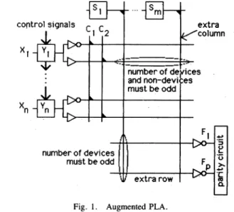
Fig. 1 showsa PLAaugmentedby adding 2 shift registers,a parity circuit, several control lines, 1 product line, and 1 sum line'. The productlines' shift register can disable all product lines but one, to allowthe effect ofa single product line on the outputs to be observed (e.g., to observe only product line "i", set
Si
to 0, and all otherSj's
to1). The other shift register is added to the input decoder so that it candirectly generatethe function independent test input sequence.When
eitherof the control lines Cl and C2 is set to 1, then allx's
and x's, respectively,are forced to zero. The extra product line is used to make both the number of devices (i.e., transistors) and nondevices (i.e.,lack of a transistor) on each bit line odd. If the original number ofproduct linesis odd, then 1 extra line (total m is even) suffices; otherwise two extra lines are used.Likewise,
the extra sum line is usedto forceeveryproduct
line(OR
array partonly)
to haveanodd numberofdevices, The parity
circuitplaced
after theoutputdecoderFig. 1. Augmented PLA.
consists of a cascade of Exclusive-OR gates which determines the parity of the output vector. Unlike the scheme in [3], [7], we do not use a second parity circuit on the product lines, which saves area.
The augmented PLA is tested with the patterns shown in Table I. We apply these test patterns in the following order, called the
'universal
test sequence," where rI represents repeated concatena- tionm n m m n m
/1 (1(2)* 171 (14) * (l)* 1Ij( )
j=I i=1 j=l j=1 i=iIj'.=I
Every new outputvectoris
compressed
into asingle parity bit,
and then this bit isExclusive-oRedwith a bit representing the cumulative parity of all previous output vectors, to obtain a new cumulative parity bit (CPB). By examining the CPB only (2n + 2m + 1) specific times, we can detect all single faults andalmostall multiple faults.Definition:
Let the term cumulative parity comparison refer to the comparison scheme shown in Fig. 2. The asterisks indicate the (2n + 2m + 1) times when the cumulative parity bit (CPB) is compared to its expected value (i.e., during 11, 1] and l3 the cumulative parity iscompared after everyclockcycle, for a total of 2m + 1 comparisons; during 14. and 15. the cumulative parity is comparedonly after every mth clockcycle,and is ignored the rest of the time, for a total of 2n comparisons). Note that thecumulative paritycomparison
scheme is function independent because the CPB sequence of length (2n + 2m + 1) is simply an alternating sequence of0'sand I's (i.e., 0101010101 * ). Hence, the fault-free CPB sequence can be generated on-line by a simple circuit, and thus does not have to be stored in (2n +2m
+ 1) bits. The nMOSimplementation
detailsarein[6]. Ifthetestpatterns wereappliedin anorder different from the "universal testsequ4ence,"
the test pattern generation circuit and the cumulative parity comparison circuit would bemore complicated and hence occupy more silicon area; thus, the universal test sequence was chosen for practical reasons. The expected parity bits of individual output vectors are derived as follows (useFig. 3).11: If the PLA isfault-free,then theoutputvector is a string of all zeros, whose parity is zero.
lj2:
If the PLA is fault-free, then each of the m output vectors has an oddnumber of l'sbecause eachproduct line in the OR array has an odd number of devices. Thus, the paritypf
each outputvector is 1. (Similarly for1>.)
14.:
Assume the PLA to befault-free. Forsimplicity, considerthe partial test patternHj(14(l),
with i being constant, which activates the crosspointson bit linexi
only.If the crosspoint (xi,j)
has a device, thenthe
product line j is pulled down to 0, whichproducesan output370
TABLEI
DEFINITIONS OFTESTPATTERNS
Y1.
i-
I i ...xn c1l 2 SI Sj
Is5j Si+I Sm
21.
g
0 0 0 1 0 1 101 112j
1 ... 1 ... 1 0 1 ... 1 0 1 .. 1oi
I 1 0.0o
1 1... 0 1 114
0115~... 1 0 1 0 1 1... 0 1 1~~~~
.I.1 ...
..of allzeroes,andthusa
parity
bit ofzero. If thecrosspoint (xi, j)
has NOdevice,
then theproduct
linej
stays at1,
which produces an output withanodd number ofones,and thusaparity
bitof1. Recallfrom
Fig.
1 thatthe number of nondevices of each bitline isodd,
therefore an odd number of l'sparity
bits arecreated for each bit line.(Similarly
for15.)
III. FAULT COVERAGE This sectionprovesthefollowingtheorem.
Theorem 1: All
single
and(1
- 2-(m2n))
of allmultiple
crosspoint, stuck,
andbridging
faults aredetectedby
thecumula- tiveparity comparison
scheme whenthe universal test sequence,,47Expected
Parity 1itsq/
OutputVector Cumulative0...0 1... *0 *0
2
o- *
odd
I ° LI 21
number* of is
*1
*0
* I
* O=mmod2
(sincemis even)
J*1 =(m 1 mod 2
* (mr+lmod2
* (m+n)mod 2 t =nmod2
odd
_
OFig2. i number
~of I's ji (n+I)mod2
ij n*Ws
*(n+i)mod2
1
oQ
ddJ~
num ber.=0
Fig. 2. Cumulative parity comparison scheme.
AT
0I
0~~~
0~~~
_t~~~~ 1
11.
2 14
0 0
in n m m n m
/1* ('])* fj
jj(1
(14)* fj(1;)j=1 i=1 j=1 j=1 i=1 j=1
is
applied.
Forexample, a PLA with n = 25 inputs and m = 50
product
terms, wouldhaveover(1
- 2-100)
of itsmultiple faults detected. Theproofispresentedbya sequenceof 8 lemmas in "dominostyle." Thismeansthat later lemmasusein theirproofsthe results of earlier lemmas. This- is possible because of the high degree of"equiva-
lence" between the faults of different faultmodels where"equiva-
lent"meansthat theoutputresponsesareidenticalgivenaspecificset ofinput
vectors. Dueto spacelimitations, mostproofsareabridged,
but fulllength proofscanbe obtained from the authorsuponrequest. Lemma 1: All single and (1 - 2-2n) of all multiple
crosspoint
faults in theAND arraycanbedetected by thetestpatternsn m n m
IIHIIH(14J)
i=1 j=1and 11
i=1 j=I(15..).
Proof:Acrosspointfaultat
(xi, j)
inverts the expected valueofproduct
linej,
hencealsoinverts theoutputparity. 14 and1.activate allmcrosspointsofabit linetoproduceonenewCPB. If thetotal number offaultson abitline iseven,the CPB indicatesnofaultsince the numbers ofdevicesandnondevices for the line remainodd. Thus, theonly multiple faults thatarenotdetectedarethose which havean even number offaults (or zero faults) on each bit line. The total number of possible multiple crosspoint faults in the AND array is2(2n)(m).Thenumberof possibleevenfaults (includingzerofaults) for
asinglebit line is2(m-1). Thus, thefraction of undetectable faults in theANDarray is: (2m-1)2n/22nm = 2-2n.c
-We do not try to improvethis fault coverage by increasing the number of comparisons of CPB's during 1. and15.fromntimestonm
times, because this renders the CPB comparison scheme
function
dependent, which requiresvery much extra hardwareto store the expectedCPB's for the individual crosspoints of theAND array.Lemma 2: All single and (1 - 2-m) of all of the multiple crosspointfaults in theORarray canbe detected by applying either
m m
i1(12) or
j=l j=l
Proof:A crosspoint fault in the product linesegmentcircled in Fig. 3 inverts the output parity. As in Lemma 1, undetectable multiple faults have an evennumber of faults perproduct line(OR
array part). The fraction of undetectable faults in the OR array is
(2P-I)m/2Pm
= 2-mLemma3: All single and all multiple extradevice faults in the input decoderaredetected when
n m n m
(14J.)
and(15 )
i=l j=l i=l j=l Fig.3. Effectsof testpatterns.
Xl"Xn Sil**Sm
A 0 0 1
B 0 1 1
are
applied.
i_10Proof:
Anextradeviceatintersection(Cl,
x,) causes bit linexi
tobeconstantly 0.
while14 isapplied.
Similarly, for (C2,£i)
and15..Hence,
anymultiple
extra device fault in the input decoder isequivalent,
inthecontext of14,
and1,
to a "Lemma1 detectable"multiple crosspoint
fault in theAND array (i.e., an odd number ofmissing
devices on eachaffected bit line). H Lemma 4: Allsingle
and all multiple missing devicefaults in theinput
decoder aredetected whenm m
J7
(1P) and JI (13)
j=1 j=1
are
applied.
Proof:
Whenthedevice at(C1, £,)
ismissing, bit linex,- has the value1while1]
isapplied.
Similarly for (C2,xi)
and13.Any multiplemissing
devicefaultinthe inputdecoder isequivalent, in the context of12
and13,
to a"Lemma2detectable" multiple crosspoint faultin theORarray(i.e.,
anoddnumberofmissing deviceson each affectedproduct
line(OR part)).
OLAlthough only
one of13 or /3 is needed to detect OR arraycrosspoint
faults(see
Lemma2), both
12 and /3 are needed to detect missingcrosspoint
faults inthe input decoder (see Lemma4).Lemma5: Undetectable multiple crosspointfaults in the OR array cannotmaskdetectable
multiple
crosspointfaults in the AND array in thecontextof/.
and15.. Also,
undetectable multiple crosspointfaults intheANDarraycannot maskdetectable multiple crosspointfaults in the OR array inthecontextof13
and/3.
Proof. /1
and 15. detectANDarray faults when the OR arraypart
of everyproduct
line hasanodd numberofdevices. UndetectableOR arrayfaults cause aneven number ofdevices in eachproductline to appearordisappear,
hence thetotal number of devices per productline remains odd. O
Lemma6: All
single
stuck-atfaults aredetectedby thecumulativeparity
comparison scheme.Proof:
There aresix cases toconsider.a)
sum line stuck-at 0: this fault is detected by1'.
The
remaining
five stuck-at fault cases are equivalent, in the contextsspecified below,
to multiple missing device (crosspoint)faults,
and thus aredetectable by Lemmas 1 and 2.b)
sumline stuck-at 1:equals
alldevices on sum linemissing, in thecontext of /3 and/3.
c) product
line stuckat0: has no effect upon sum lines, hence this fault- = all devices in the OR array part of the product linemissing,
in thecontextof/3 andI/3.
id) product
line stuck-at 1: equals all devices in ANDpart
ofproduct
linemissing,
context 14 and 15..e)
bit line stuckat0:hasnoeffect
uponproduct lines, hence this faultequals
all devicesonthe bitlinemissing,in thecontextof1/
and15..
f)
bit line stuck-at 1: sinceall product lines which thestuck-at 1 bit line connects with are forced to 0, this fault equals all the affectedproduct
linesstuck-at 0(i.e.,
multiple Case c) above). C: Lemma7:Atleast(1
- 2 -(m+2n))
of allmultiplestuckfaultscan bedetectedby
the cumulativeparity
comparisonscheme.Proof:.
Therearethreecases toconsider.Case
(c
+ e +f.): The three fault types: product line stuck- at0,
bit line stuck-at0,
and bit line stuck-at 1, combined intomultiple
stuck faultsequal
always detectable multiple crosspointfaults,
since both bit linesand OR array parts of product lines haveonly
odd numbers ofcrosspoint
faults.Case
(b
+d.):
Whensum linestuck-at 1 and product line stuck-at 1aremultiple
stuckfaults, then(1
- 2-(m+2n)) of themequal multiple crosspoint
faultswithodd numbersofbit/productlinefaults.
Case
(a
+.):
In thecontextof/2
and/3
Ithe sumline stuck-at0 fault = multipleextradevice fault where each faultysumlinehas a device at every one ofits crosspoints; now use Lemma2. H Lemma 8: All single and at least
(1
- 24m+2n))
of all multiple bridgingfaults aredetected by the Cumulative Parity Comparison scheme.Proof:
There are five cases to consider: 1) two product lines shorted together, 2) two bit linesshorted
together, 3) a productline and a bit line shorted together, 4) a product line and a sum line shorted together, and 5) two sumlinesshorted
together.The first four cases are equivalent to stuck-at faults.
1) Since a bridging fault (in nMOS) causesboth lines to be 0 when at least one of them is 0, bridged product lines equal stuck-at 0 product lines inthe contextof/3 and
/3.
Hence, Lemmas 6c) and7-c), e),and f)assuredetectionofallsingleand allmultiple pairedproduct line bridging faults.2) Bridged bit lines equal stuck-at 0 bit lines, context 1. and
/5..
Now use Lemmas 6-e) and 7-c), e), and
f).
3) In the contextof /3 and
/3,
allbitlinesnormallyhavethe value0, so any product lines bridged with bit lines equal stuck-at 0 product lines. Now use Lemmas 6-c) and 7-c), e), and f).4) In the contextof
11, 2,
and/3,
product lines almostalways equal 0, so any sum linesbrid'ged with
product lines are almost always equal to stuck-at0 sum lines-. Now use Lemmas 6-a) and7-a).
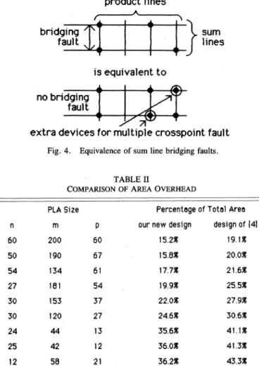
5) If 2 sum linesA and B arebridged, then theircommon value V is the logical AND of A and B. In the context of
/2
and3,
Vhasthe value 1 only when neither line A and Bhas a device on thecurrently active product line. Thus, this bridging fault equals a multiple crosspoint fault where both A and B have extradevices everywhere, except along the productlines where bothA and B wereoriginally without devices, as shown in Fig. 4. Now use Lemma 2. OThese lemmas complete the proof of Theorem 1. It is also possible to show that almost all physical failures in the extra hardware are detected by thecumulativeparity comparison scheme. To prove this statement we must specify the exact nature of these "physical failures," but such a formal proof is very long and is therefore omitted. By inspection of Fig. 1, it is evident that physical failures in the augmented input decoder and in the product lines' shift register will cause bit lines and product lines, respectively, to have wrong values sometimes, and hence such failures will seem equivalent to various bit line and product line faults. Similarly, physical failures in the parity circuit (i.e., output response compressor) will generate wrong parity values sometimes, and such failures will seem equiva- lent to various sum line faults. For greater testability, we can program the OR array segment of the extra product line (recall that only the AND array segment of the extra product line is used to force bit lines to have certain parities, while the OR array segment is unused) to guarantee that all 4 combinations {00, 01,
10,
11} are applied to every Exclusive-OR gate in the parity circuit (since a nonfaulty pair of sum lines may generate only 2 or 3 of the combinations { 00, 01,10,
ll}).
IV. CONCLUSION
A new approach to design low overhead and high
fault
coverage self-testing PLA's has been presented. Thefaultcoverage isproven to consist of all single faults and atleast(1
- 2-(m+2))
of allmultiple
faults of crosspoint, stuck, and bridging types. We claim that our design provides a greater fault coverage than all known BISTdesigns, since the papers describing these other designsdo not presentproofs of coverage of as many different kinds of faults as wedo.A companion paper [6] describes the implementationdetailsofthis approach and compares it with other previously published designs. Due mainly to the very "regular" nature ofthe cumulative
parity
scheme used in our approach, theadditional overhead requirements are quite small compared to all other known designs.Table II lists the percentage overhead for various PLA's. For large PLA's, the overhead can be as small as 15percent ofthetotal PLAarea,
which may be acceptable in such cases. This overhead includes all extra372
COMPUTERS, C-36, 3,
product lines
-.
-w I
I
t - t aT
is equivalent to
IL L I
The ComparisonApproach toMultiprocessor Fault
Diagnosis
}sum lines
T o
;;W
Textra devices for multiple crosspoint fault
Fig.
4.Equivalence
ofsumlinebridging
faults.TABLE II
COMPARISONOFAREA OVERHEAD
ANTONT. DAHBURA, KRISHAN K.
SABNANI,
AND LINDA L. KINGAbstract-In this correspondence a system-level, comparison-based strategy foridentifying faulty processors in a multiprocessor system is described. Unlike other strategies which have been proposed in the literature, the comparisonapproach ismoreefficient and relieson more
realistic assumptions about the system under consideration. The new
strategyis shown tocorrectly identify thesetoffaultyprocessors witha
remarkablyhighprobability, making itanattractive andviable addition or alternative topresent faultdiagnosistechniques.
Index Terms-Comparison assignment, diagnosis, fault tolerance, multiprocessorsystems, self-diagnosable systems,syndrome.
I.
INTRODUCTIONTheproblemofidentifying failuresinmultiprocessorsystems has
PLA Size Percentage ofTotalArea become importantwith both thegrowing
complexity
of thesystems
design design [41 and the critical application areas in which they
used. Further-
more, the classical techniques for identifying system-level
failures,
60 200 60 15.2% 19.1% such as error-detecting codes and massive
redundancy
withvoting,
15.6% are unable to yield the high level of reliability required without a
tremendous amount of hardware overhead and/or performance
54 134 61 17.7% 21.6% degradation.
27 181 54 19.9 25.5% Consequently, severalelegant, albeittheoretical, models have been
proposed as a foundation on which to construct more effective 30 153 37 22.0% 27.9% system-level faultdiagnosis strategies [1], [4]. The classical model
30 120 27 24.6% 30.6% forconsidering system-level failures in distributedcomputer
systems
isthatintroduced by Preparata, Metze, andChien [1]. In thePMC 24 44 13 35.6% 41.1% model,aset ofprocessorsisassembledsuchthateachprocessortests 25 42 12 36.0% 41.3% asubset of theothers. It isassumedthatabounded size subset of the
12 58 21 36.2% 43.3% processors is faulty and that the test results generated by faulty
*___ _ _ _ ___ processors are unreliable. Hakimi and Amin [2] characterized the class of testingassignments such that thesetoffaulty processors can
testing
testing
circuitry andcircuitry, andt is based on actual nMOS layouts [6].
Anexact beresults, uniquely assuming identified
thatonthethe
number ofbasis of any faulty given
processorscollection of does test
notcomparison (see
TableII)
ofarea overhead canbe madeonly
with exceedthegivenbound. AnO(n2.5) algorithm foridentifying
theset[4],
where theoverheadiscalculated withrespecttoactuallayouts.
offaulty in such systemshas beengivenbyDahburaand Allotherpublished designs report
overheadintermsofthe number of Masson[3] and dlstrlbuted diagnosisalgorithm hasbeengivenby
additional
logic
gates, which does not reflect the actual areaoverhead. However, bysimplycomparing the quantities and types of Kuhl andReddy [10].
components usedin eachdesign, iteasily follows thatour newdesign Inthiscorrespondence, wetakeanewapproachto the problem of
uses lessarea. system-level fault identification. We introduce a simple algorithm
which, while notguaranteedtosuccessfully identify thesetoffaulty REFERENCES processorsinasystem,will dosowitha
remarkably high probability.
Testing, The advantages of our approach are as follows: 1) we make more
Williams Ed. Amsterdam, The Netherlands: North-Holland, 1986, realistic assumptions about the system, and 2) the strategy is
pp. 65-93. performed inat mostO(n2)operations,
making
itmoreefficientthan[2] W.Daehn and J. Mucha, "A hardwareapproachtoself-testingoflarge any other. These issues aredescribed in detail in the
following.
programmable logic arrays," IEEETrans. Comput., vol. C-30,pp. Although the PMCmodelisareasonable
starting point
forsystem-
829-833, Nov. 1981. level approaches to fault diagnosis, it is plagued
by
severalrigid
[3] H. Fujiwara and K. Kinoshita, "A design of programmable logic assumptionsaboutthenatureoffaults and tests.Firstofall,the modelarrayswith universal tests," IEEE Trans. Comput., vol. C-30,pp. reliesontheexistence oftestswhich the processors administertoone
823-828, Nov. 1981.
1 othe Furteroeof tests area ss ors comlete,to a
[4] K. A.Hua, J.-Y. Jou, and J. A. Abraham, "Built-in tests for VLSI another- Furthermore, the tests areassumedto becomplete,in thata finite-state machines," in Dig. 14thInt. Symp. Fault-Tolerant fault-free
Comput. (FTCS-14), 1984,pp. 292-297. processor which it tests. Secondly, the faults are assumed to be [5] S. Z. Hassanand E. J. McCluskey, "Testing PLA's usingmultiple permanent, meaningthatafaultyprocessorexhibits
logical
behaviorparallelsignatureanalyzers," inDig. 13thInt. Symp.Fault-Tolerant which is consistent and different from that which is
specified.
Comput., (FTCS-13), 1983, pp. 422-425. Thirdly, the tests are assumed to be run
alternately
withsystem
[6] R.Treuer, H. Fujiwara, and V. K. Agarwal, "Implementingabuilt-in workload,allowingfaultswhichmanifestthemselves between
testing
self-test PLAdesign,"
IEEE Des. TestComput.,
vol.2,
pp. 37-48,Apr. 1985.
[7] S.
Yajima
andT. Aramaki,"Autonomously
testableprogrammable
logicarrays,"
inDig. Ilth Int. Symp.
Fault-TolerantComput.
(FTCS-11),
1981,pp. 41-43.ManuscriptreceivedJuly 31, 1985; revised December22, 1986. Theauthors arewith AT&T BellLaboratories, Murray Hill, NJ07974. IEEELog Number8612064.
0018-9340/87/0300-0373$01.00 © 1987IEEE
bridging
fault
no bridging
fault
-