A Functional Test Method for State Observable FSMs
Toshinori Hosokawa and Hideo Fujiwara
College of Industrial Technology, Nihon University
1-2-1, Izumicho, Narashino, Chiba 275-8575, Japan
Graduate School of Information Science, Nara Institute of Science and Technology (NAIST)
8916-5, Takayama, Ikoma, Nara 630-0192, Japan E-mail: [email protected], [email protected]
Abstract
Scan testing is the most popular test method for VLSIs. However, because the shift operation during the test causes over testing, the yield loss of VLSIs may occur. It is important to test VLSIs using the given function. On the other hand, it is well known that state-observable and completely specified FSMs are completely functionally tested by performing all possible state transitions. This method, however, drastically increases the test cost. This paper proposes two test methods, a fault independent functional test method and a fault dependent test generation method, for state-observable FSMs to reduce the yield loss while improving the test quality over scan testing at a reasonable test cost. Fault dependent test generation is based on a single pattern test for a logical fault model and a two- pattern test for a timing fault model. Experimental results using MCNC'91 benchmark circuits show that the proposed method reduces the average area by 13.2% while increasing the state transition coverage 4.3 times by using only 29.4% additional test sequences compared with the conventional non-scan test method for FSMs.
keywords : State-observable FSMs, Constrained ATPG, Over testing, Fault dependent test generation, Fault independent functional test, State transition coverage
1. Introduction
In recent years, VLSI (Very Large Scale Integrated circuit) testing has become more important because the number of gates on VLSIs is rapidly increasing and their complexity is growing with advances in semiconductor technology. Currently, scan testing for the stuck-at fault model [1, 2] is one of the most popular test methods for VLSIs. However, it has been reported that scan testing for the stuck-at fault model may not detect defective VLSIs [4] and
delay testing [3] and at-speed functional testing can effectively improve test quality.
VLSI design methodologies employing hardware description languages have recently been adopted to reduce VLSI design time. VLSIs are designed at RTL (Register Transfer Level) and the RTL circuits consist of a data path part and a controller part. The data path contains a hardware element (e.g., registers, multiplexers, and operational modules) and signal lines and the controller is represented by an FSM (finite state machine). A non-scan based DFT (Design For Testability) method of data path parts is proposed in [5], while a non-scan based DFT method for controller parts is proposed in [6]. At-speed testing is easily applicable and test patterns for a stuck-at fault model are completely generated by the non-scan based DFT methods. As mentioned above, if at-speed functional testing and/or delay testing are applied to VLSIs with a non-scan based DFT, the test quality can be further improved. It was reported in [7] that state-observable and completely specified FSMs are thoroughly functionally tested by performing all of the state transitions. Thus, complete at-speed functional testing can be applied to FSMs whose states are made observable by performing all of the state transitions at-speed.
As mentioned above, scan testing is currently the most popular test method. Scan testing is not based on the function, but the structure of the circuit. In this method, the states of the circuits are transferred to invalid states by shift operation during the testing in order to detect faults. This method is considered over testing and a yield loss of VLSIs may occur. It is important to test using the function, and the test method described in [7] can functionally test state- observable FSMs completely, but at a dramatically increased test cost.
This paper proposes two test methods, a fault independent functional test method and a fault dependent test generation method, for state- observable FSMs in order to reduce the yield loss
IEEE 6th Workshop on RTL and High Level Testing, pp. 123-130, July 2005.
caused by over testing while improving the test quality over that of scan testing within a reasonable test cost. This paper also proposes state transition coverage as the measure of test quality for functional testing. State transition coverage is defined as the ratio of the number of state transitions executed by a test sequence to the entire number of state transitions. Moreover, problems are formulated from the points of view of both fault independent functional tests and fault dependent tests for state-observable FSMs, and test generation methods are proposed to solve these problems.
This paper is organized as follows. In Section 2, a functional testing method for state-observable and completely specified FSMs is detailed. In Section 3, the optimization problems for both functional and fault dependent tests are formulated for state- observable FSMs, and their test generation methods are proposed. The proposed methods are applied to MCNC’91 FSM benchmarks [9] in Section 4, and the experimental results are presented. Finally, Section 5 concludes the paper and discusses future research possibilities.
2. Functional Test for State-Observable
and Completely Specified FSMs
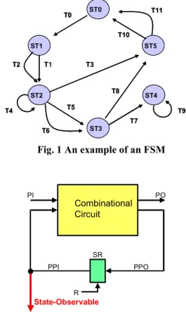
Fig. 1 shows an example of an FSM. In this figure, ST0 through ST5 and T0 through T11 show the states and the input values of the state transitions (the value of each primary input
∈
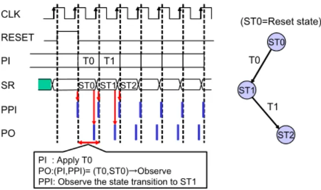
{0, 1, X}, where X denotes don’t care), respectively. The DFT makes the outputs of the status registers in the FSM observable and a synchronous sequential circuit is synthesized from the FSM using logic synthesis. Fig. 2 shows the logic circuit model that corresponds to an FSM after logic synthesis. Because the PPI, which is the outputs of the status registers, is observable in this figure, the PPI is treated as the primary output. PI, PO, SR, PPI, PPO, and R denote primary inputs, primary outputs, status registers, pseudo primary inputs (the outputs of the status registers), pseudo primary outputs (the inputs of a the status registers), and a reset input, respectively. The combinational circuit part is called the test generation model because combinational test generation is applied to the circuit.It has been reported that state-observable and completely specified FSMs are completely functionally tested by performing all of the possible state transitions [7]. Thus, complete at-speed
functional testing can be applied to FSMs whose states are made observable by performing all of the state transitions at-speed.
3. A Test Method for State-Observable
FSMs
From now on, state-observable and completely specified FSMs will only be called state-observable FSMs due to simpkification.
3.1 Preliminaries
(Definition 1: Functional test for state-observable FSMs)
In this test, the PI value is applied to a state- observable FSM, the state is then transferred from the current state to the next state, and the resulting PPI and PO values are observed. A series of these procedures are referred to as a functional test for state-observable FSMs.
Fig. 1 An example of an FSM
Fig. 2 A logic model for a state-observable FSM
ST0
ST1
ST4
ST3
ST5
ST2 T0
T1 T3
T4 T5
T10
T7
T9 T2
T6
T11
T8 ST0
ST1
ST4
ST3
ST5
ST2 T0
T1 T3
T4 T5
T10
T7
T9 T2
T6
T11
T8
Combinational Circuit
State-Observable
PO PI
SR
PPI PPO
R
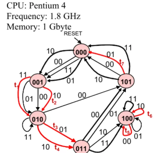
Example 1: In Fig. 1, T0 is applied to state ST0 on the state-observable FSM and the state is transferred from ST0 to ST1. T1 is then applied, and the state is transferred from ST1 to ST2. Fig. 3 depicts the timing chart for this functional test for a state- observable FSM. R is activated and the values of the status registers are initialized to ST0 at the first cycle. At the second cycle, T0 is applied and the values of the POs for (PI, PPI)=(T0, ST0) are observed just before the rising edge of the clock. Here, (PI, PPI) denotes that the value of PI is applied to the PPI value (state) for a state-observable FSM. Moreover, the PPI value is observed after the rising edge of the clock. Thus, it is verified that the state is successfully transferred from ST0 to ST1. At third cycle, T1 is applied and the PO values for (PI, PPI) =(T1, ST1), which are observed just before the rising edge of the clock. The resulting PPI value is observed after the rising edge of the clock. Thus, it is verified that the state is successfully transferred from ST1 to ST2. (Definition 2: FSM test generation graph)
An FSM test generation graph is a directed graph G(V, E, r, s) where a vertex v ∈ V denotes a state. Each vertex has a label s: V → A (A={PPI1PPI2… PPIm}, PPI1, PPI2,…, PPIm ∈ {0, 1}, where m denotes the number of status registers). The label s indicates the state assignment. For any vertices u, v
∈ V, an edge (u, v) ∈ E denotes the state transition from u to v, and each edge has a label r: E → B (B={PI1PI2…PIn}, PI1, PI2, …, PIn∈ {0, 1}, where n denotes the number of primary inputs). The label indicates the input values for a state transition.
Example 2: Fig. 4(a) shows an example of the state- observable FSM and Fig. 4(b) shows an example of an FSM test generation graph. A code is assigned to each state in Fig. 4(b), and input values containing
“don’t care” for a state transition are expanded into those without “don’t care.” (ST0, ST1) and XX, represented by a cube, are expanded into four edges and 00, 01, 10, and 11 are represented by vectors.
(Definition 3: State transition coverage)
State transition coverage is defined as the ratio of the number of state transitions executed by a test sequence to the total number of state transitions. When state transitions are executed by a test sequence, it is referred to as the state transitions are covered by the test sequence. In this paper, only state
transitions specified in an FSM are used to calculate the state transition coverage. On state-observable FSMs, the input value for each state transition is represented using two types of notation. One notation is a cube that consists of 0’s, 1’s, and don’t cares (Xs). The other notation is a vector that consists of 0’s and 1’s. While generating an FSM test generation graph, state transitions and their input values initially represented by a cube in a state-observable FSM are expanded into state transitions and input values that are represented by a vector. If the input value for a state transition includes k don’t cares in an FSM, the state transition is expanded into 2k state transitions in an FSM test generation graph. Thus, state transitions with an input value represented by a vector in an FSM test generation graph are used to calculate the state transition coverage. State transition coverage is then used as a measure of the test quality for a functional test.
Fig. 3 A functional test for a state-observable FSM
Fig. 4(a) A state-observable FSM
PI : Apply T0
PO:(PI,PPI)= (T0,ST0)→Observe PPI: Observe the state transition to ST1
ST0
ST1
ST2 CLK
RESET
ST0 ST1 ST2 SR
T0
T1
PI T0 T1
PPI PO
(ST0=Reset state)
ST0
ST1
ST2
ST3
ST4 ST5 RESET
XX
X1 X0 00
01 10 11
0X
1X XX XX
Fig. 4(b) An FSM test generation graph for a state-observable FSM
Example 3: When the test sequence (11, 00, 00) is applied to the FSM test generation graph in Fig. 4(b) on the current state 000, the state transition coverage is 12.5% (3/24).
(Definition 4: Detectable stuck-at faults on valid states)
When a state is defined in a state-observable FSM and is reachable from the reset state, the state is called a valid state. Stuck-at faults detected by performing a state transition on a current state are called detectable stuck-at faults on valid states. Example 4: The input value for state transition 00 is applied to the valid state 001 shown in Fig. 4(b), and the subsequent state 010 and output value are observed. Stuck-at faults detected by the above- mentioned procedures are detectable stuck-at faults on valid states.
(Definition 5: Detectable delay faults on the transition between valid states)
The transition between valid states refers to performing state transitions between valid states in state-observable FSMs. After a transition between valid states, delay faults detected by performing a continuous state transition are defined as detectable delay faults on the transition between valid states. Example 5: The input value for state transition 11 is applied to the valid state 000 shown in Fig. 4 (b), and the state is transferred to valid state 001. Next, the input value for state transition 00 is continuously applied to valid state 001, and the subsequent state 010 and output value are observed. Delay faults detected by the above-mentioned procedures are
detectable delay faults on the transition between valid states.
3.2 Fault Independent Functional Test Method State-observable FSMs are considered to be completely functionally tested for a specified function by performing all of the state transitions. The following two problems are formulated for a functional test of state-observable FSMs.
(Formulation 1a)
Input: a state-observable FSM
Output: a test sequence such that the state transition coverage is 100% (All state transitions in the FSM test generation graph are performed.) Optimization: minimizing the test length
The test generation for Formulation 1a does not use ATPG (Automatic Test Pattern Generation) for a specific fault model. An FSM test generation graph is generated from the state-observable FSM and it searches the path so that all of the edges are traversed at least once. If the path length is minimized, the test length is also minimized. This test sequence can functionally test a state-observable FSM completely, although this method generates a huge amount of test sequences, causing the test cost to drastically increase. (Formulation 1b)
Input: a state-observable FSM
Output: a test sequence such that state transitions with an input represented by a cube and state transitions with an input represented by a vector in a state observable FSM are covered (Hence, on each state transition with an input represented by a cube, at least one state transition from among the corresponding state transitions in the FSM test generation graph is performed.)
Optimization: minimizing the test length
The test of Formulation 1b aims at improving the quality of the functional test by formulating a more reasonable test length. The test generation for this method also does not use ATPG for a specific fault model. An FSM test generation graph is generated from a state-observable FSM. When the graph is generated, each state transition with an input represented by a cube is expanded into state transitions with inputs represented by vectors. The method then searches the path so that all of the original state transitions with an input represented by a vector and at least one state transition from among
000
001
010
011
100 101 RESET
00
01 00 00
01 10 11
00
10 01
11 00 01 10
11
10
01
11 00
10 11 01
10 11
the expanded state transitions are traversed at least once. If the path length is minimized, the test length is also minimized. This test generation is expected to have a longer test length, but the state transition coverage becomes higher than the fault dependent test generation formulated in the next sub-section. 3.3 Fault Dependent Test Generation Method
In this sub-section, problems are formulated for both one pattern testing for a logical fault model and two pattern testing for a timing fault model on state- observable FSMs. In this paper, a stuck-at fault model is used as the representative of one pattern testing and a delay fault model is used as the representative of two pattern testing. The purpose of these test generations is to reduce the yield loss caused by over testing while maintaining a high quality test sequence. Problems are formulated for a stuck-at fault model and a delay fault model in the following two test generations.
(Formulation 2a) Input:
- a state-observable FSM
- a test pattern set with 100% stuck-at fault efficiency
Output: a test sequence for a state-observable FSM so that all detectable stuck-at faults on valid states are detected
Optimization: minimizing the test length
After logic synthesis, a combinational circuit part (test generation model) is extracted from the synthesized sequential circuit. The valid states are assigned to the PPI values as constraints. A constrained ATPG is performed on the stuck-at faults for a test generation model and a test pattern set is generated. After that, an FSM test generation graph is generated and test patterns are assigned to the corresponding edges of an FSM test generation graph. Finally, paths are searched on the FSM test generation graph so that all of the edges where test patterns are assigned are traversed at least once. If the path length is minimized, the test length is also minimized. For this test generation, it is expected that the state transition coverage decreases, but the test length become shorter than those for the functional test in Formulation 1b.
Example 6: Fig. 5 shows an FSM test generation graph that is generated from the state-observable FSM shown in Fig. 4(a) and a test pattern set with
100% stuck-at fault efficiency for the test generation model. Each test pattern is assigned to the corresponding edge in this graph. For example, t1 is assigned to the edge that represents the state transition from the state 001 through the input value 11.
(Formulation 2b) Input:
- a state-observable FSM
- a two test pattern set with 100% delay fault efficiency
Output: a test sequence for a state-observable FSM so that all detectable delay faults on the transition between valid states are detected Optimization: minimizing the test length
After logic synthesis, a time expansion model [10] for two time frames is generated from a synthesized sequential circuit. The valid states are assigned to the PPI values as constraints. A constrained ATPG for delay faults is performed for the time expansion model and a two test pattern set is generated. Because the delay fault test generation for state-observable FSMs is a future work, the test generation method is not discussed in this paper.
4. Experimental Results
The test generation methods for Formulations 1a, 1b, and 2a were implemented and were applied to MCNC’91 benchmark circuits [9].
The platform used for the experiments is as follows.
CPU: Pentium 4 Frequency: 1.8 GHz Memory: 1 Gbyte
Fig. 5 An FSM test generation graph for stuck-at fault testing
000
001
010
011
100 101 RESET
00
01 00 00
01 10 11
00
10 01
11 00 01 10
11
10
01
11 00
10 11 01
10 11
t1
t2
t3
t4
t5 t6 t7
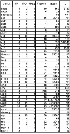
The characteristics of MCNC’91 benchmark circuits are shown in Table 1. In this figure, Circuit,
#PI, #PO, #Reg, #Vertex, #Edge, and TL denote the circuit names, the number of primary inputs, the number of primary outputs, the number of status registers, the number of states, the number of state transitions and the test length with 100% state transition coverage generated by the test generation of Formulation 1a, respectively. “NA” indicates that the test generation was not completed within 10 hours. It was discovered that extremely large test lengths and CPU times were required to perform a complete functional test. In these experiments, FSMs were made state-observable by DFT and the three test generations were performed for state-observable FSMs.
The logic syntheses for the FSMs were performed by the Synopsys Design Compiler® and the test generations for the combinational circuits were performed by Synopsys TetraMax®.
Table 2 compares the experimental results for the proposed methods with those for [6], denoted by
“JETTA’00” in the table. In [6], testing for both valid and invalid states was performed for FSMs and stuck-at faults were completely tested. “Proposed methods” denotes the experimental results of the proposed methods. “1b” denotes the experimental results of the functional test method for Formulation 1b and “2a” denotes the experimental results of the stuck-at fault test generation method for Formulation 2a. Circuit, FE, Area, TL, #CE, STC, and FC denote the circuit name, the stuck-at fault efficiency, the area of synthesized sequential circuit with DFT that was calculated based on the standard library for logic synthesis, the test length, the number of edges covered by the test sequence, the state transition coverage, and the stack-at fault coverage, respectively.
Compared to “JETTA’00,” “2a” reduced the area by 1.9 to 27.7% (average 13.2%), while increasing the state transition coverage from 1.5 to 10.8 times (average 4.3 times) by using -18.1 to 160.4% (average 29.4 %) additional test sequences. After the state is transferred to a test state in [6], the PI values of the test patterns are applied one after another while holding the PPI value in the status registers. Therefore, the path is searched so that all of the test states are traversed at least once. This method reduced the test length, making it smaller than that of
“2a.” On the other hand, because the stuck-at faults
were tested by performing state transitions in “2a,” the state transition coverage was higher than for
“JETTA’00.” As for the area, “2a” made the outputs of status registers observable by DFT, while
“JETTA’00” made the inputs of status registers observable. Moreover, “JETTA’00” added the circuit that was going to be transferred to invalid test states, the multiplexers switched the valid state transitions and the invalid state transitions, and the hold function of status registers by DFT. Therefore, “2a” reduced the area compared to “JETTA’00.”
Test length of “1b” compared “2a” was 1.3 to 13.3 times longer (average 3.4 times), and the state transition coverage was 0.5 to 8.2 times higher (average 1.8 times). “1b” detected all of the detectable stuck-at faults on the valid states for the FSMs, but the ratio of detected faults to detectable stuck-at faults on the valid states was 92.4 to 97.7% for cse, ex6, lion, opus, s386, and train11.
5. Conclusion
This paper proposed both a fault independent functional test method and a fault dependent test generation method for state observable FSMs. This paper also proposed state transition coverage as the measure of test quality for a functional test. The following conclusions were obtained from applied the proposed methods to MCNC’91 benchmark circuits.
(1) The test generation of Formulation 2a reduces the average area by 13.2% while increasing the state transition coverage by 4.3 times, while adding only 29.4% test sequences compared with [6].
(2) The functional test of Formulation 1b increases the average state transition coverage 1.8 times by using 3.4 times additional test sequences compared with that of Formulation 2a.
Future work includes proposing a test generation for a delay fault model in state-observable FSMs (Formulation 2b).
Acknowledgements
The authors would like to thank Mr. Seiji Hamamoto of System JD Co., Ltd. for his invaluable discussion and comments.
Table 1 FSM benchmark characteristics
References
[1] H. Fujiwara, “Logic Testing and Design for Testability,” The MIT Press, 1985.
[2] M. Abramovici, M. A. Breuer, and A. D. Friedman, “Digital systems testing and testable design,” IEEE Press, 1995.
[3] A. Krstic, and K.-T. Cheng, “Delay Fault Testing for VLSI Circuits,” Kluwer Academic Publishers, 1998.
[4] P.C. Maxwell, R.C. Aitken, R. Kollitz, and A. C. Brown, “IDDQ and AC Scan: The War Against Unmodelled Defects,” Proc. of IEEE Int. Test Conf., pp.250-258, Oct., 1996.
[5] H. Wada, T. Masuzawa, K.K. Saluja, and H. Fujiwara, “Design for strong testability of RTL data paths to provide complete fault efficiency,” Proc. of 13th Int. Conf. on VLSI Design, pp.300-305, 2000.
[6] S. Ohtake, T. Masuzawa, and H. Fujiwara, "A non-scan approach to DFT for Controllers Achieving 100% Fault Efficiency," Journal of Electronic Testing: Theory and Applications (JETTA), Vol. 16, No. 5, pp.553-566, Oct. 2000. [7] H. Fujiwara, and K. Kinoshita, “Design of Diagnosable Sequential Machines Utilizing Extra Outputs,” IEEE Trans. on Computers, Vol. C-23, pp.138-145, Feb., 1974.
[8] T. Sasao, “Switching Theory for Logic Synthesis,” Kluwer Academic Pub., 1999. [9] S. Yang, "Logic synthesis and optimization
benchmarks user guide," Technical Report 1991-IWLS-UG-Saeyang, Microelectronics Center of North Carolina, 1999.
[10] T. Inoue, T. Hosokawa, T. Mihara,, and H. Fujiwara, “An optimal time expansion model based on combinational ATPG for RT level circuits”, IEEE Proc. Asian Test Symp., pp.190- 197 , Dec. 1998.
A
A
A A
A A A A A A A A A A A A A A A A L
C # # # #V #
Table 2 Experimental results
L #C C C L #C C C
. % . % . % . % . % . % . %
. % . % . % . % . % . % . %
. % . % . % . % . % . % . %
. % . % . % . % . % . % . %
. % . % . % . % . % . % . %
. % . % . % . % . % . % . %
. % . % . % . % . % . % . %
. % . % . % . % . % . % . %
. % . % . % . % . % . % . %
. % . % . % . % . % . % . %
. % . % . % . % . % . % . %
. % . % . % . % . % . % . %
. % . % . % . % . % . % . %
. % . % . % . % . % . % . %
. % . % . % . % . % . % . %
. % . % . % . % . % . % . %
. % . % . % . % . % . % . %
. % . % . % . % . % . % . %
. % . % . % . % . % . % . %
. % . % . % . % . % . % . %
. % . % . % . % . % . % . %
. % . % . % . % . % . % . %
. % . % . % . % . % . % . %
. % . % . % . % . % . % . %
. % . % . % . % . % . % . %
. % . % . % . % . % . % . %
. % . % . % . % . % . % . %
. % . % . % . % . % . % . %
. % . % . % . % . % . % . %
. % . % . % . % . % . % . %
. % . % . % . % . % . % . %
. % . % . % . % . % . % . %
. % . % . % . % . % . % . %
. % . % . % . % . % . % . %
. % . % . % . % . % . % . %
. % . % . % . % . % . % . %
. % . % . % . % . % . % . %
. % . % . % . % . % . % . %
. % . % . % . % . % . % . %
. % . % . % . % . % . % . %
. % . % . % . % . % . % . %
L #C C A
C
A' [ ] A