A Non-Scan DFT Method for Controllers to Achieve Complete Fault Efficiency
Satoshi Ohtake Toshimitsu Masuzawa Hideo Fujiwara Graduate School of Information Science, Nara Institute of Science and Technology
8916-5, Takayama, Ikoma, Nara 630-0101, Japan E-mail: satosi-o, masuzawa, fujiwara @is.aist-nara.ac.jp
Abstract This paper presents a non-scan design-for-test- ability method for controllers that are synthesized from FSMs (Finite State Machines). The proposed method can achieve complete fault efficiency: test patterns for a combi- national circuit of a controller are applied to the controller using state transitions of the FSM. In the proposed method, at-speed test application can be performed and the test ap- plication time is shorter than previous methods. Moreover, experimental results show the area overhead is low.
1. Introduction
Testing of large VLSI circuits is a well-known hard prob- lem. It is necessary to reduce the cost of testing and to en- hance the quality of testing. The cost of testing is estimated by test generation time and test application time. The qual- ity of testing is estimated by fault efficiency1. Therefore, we have to reduce test generation time and test application time and to enhance fault efficiency.
For combinational circuits, efficient test generation algo- rithms are proposed[1] to generate test patterns and com- plete (100%) fault efficiency can be achieved. On the other hand, for sequential circuits, any test generation al- gorithm generally can not attain complete fault efficiency within reasonable time since the search space of test gen- eration grows explosively as the number of flip-flops (FFs) increases. Therefore, several design-for-testability (DFT) methods for sequential circuits are proposed.
One of the most commonly used DFT methods for se- quential circuits is the full-scan DFT method[1]. A sequen- tial circuit consists of a combinational logic block and a state register (set of FFs). In order to control and to observe the value of the state register, the full-scan DFT method re- places each FF in the state register with a scannable FF. By considering the state register as primary inputs/outputs, a combinational test generation algorithm can be used to ob- tain a test sequence with short test generation time and to achieve complete fault efficiency. However, as the num- ber of FFs of the state register becomes larger, test applica-
1Fault efficiency is the ratio of the number of faults detected or proved redundant to the total number of faults.
tion time becomes longer because of scan in/out operations. Furthermore, this method excludes at-speed test application (test application at the operational speed). Maxwell et al.[2] show that the number of physical faults detected by apply- ing test patterns for stuck-at faults at the operational speed is larger than that at slow speed. Therefore, at-speed test application is important.
A non-scan DFT method which allows at-speed test ap- plication is proposed by Patel et al.[3]. In their method, for a sequential circuit, a set of FFs in the state register is selected to control the values of those FFs directly from pri- mary inputs. To make those FFs controllable, multiplexers are inserted in front of those FFs. If the number of primary inputs is larger than or equal to the number of FFs in the state register, all the FFs in the state register can be con- trolled from primary inputs, and thus a combinational test generation algorithm can be used. On the other hand, if the number of primary inputs is smaller than the number of FFs in the state register, some FFs are not directly controllable from primary inputs. Therefore, a sequential test generation algorithm must be used, and hence complete fault efficiency is not always guaranteed.
In this paper, we present a non-scan DFT method for controllers which guarantees complete fault efficiency. In this method, test patterns for a combinational logic block of a controller is generated using a combinational test genera- tion algorithm. Each generated test pattern consists of the values of primary inputs and the state register. If the value of the state register can be stored by state transitions from the reset state, the test pattern can be applied using the state transitions. However, some test patterns may contain values of the state register that cannot be stored by state transitions from the reset state. We call states corresponding to such values invalid states. We append an extra logic to the con- troller so that it generates those invalid states. The proposed method has the following advantages:
1. Test patterns can be generated by combinational test generation algorithms.
2. Complete fault efficiency can be achieved.
3. Test application time is shorter than previous methods. 4. At-speed testing can be performed.
IEEE the 7th asian test symposium (ATS'98), pp. 204-211, Dec. 1998.
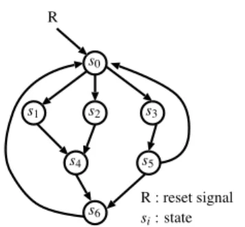
s1 s2 s3
s4 s5
s6 s0 R
si: state R : reset signal
Figure 1: A finite state machine (FSM).
In this paper, we also evaluate the effectiveness of the proposed method by experiments with MCNC’91 FSM benchmarks. The experimental results show that the pro- posed method is effective and the area overhead is low.
This paper is organized as follows: Section 2 gives some definitions. Section 3 describes an overview of our ap- proach. Section 4 presents a non-scan DFT method for con- trollers. Section 5 presents a test generation method and a test application method. Section 6 shows comparison of the proposed method with previous methods and presents experimental results.
2. Preliminaries
In register transfer level (RTL) description, a VLSI cir- cuit generally consists of a controller and a datapath. In this paper, we consider only controllers. A controller is described by a finite state machine (FSM). An FSM (see Figure 1) has one reset state, and it goes to the reset state regardless of the current state when reset signal is supplied. A controller is realized by a sequential circuit (see Figure 2) which is synthesized from an FSM by logic synthesis. A se- quential circuit consists of a combinational logic block (CC) and a state register (SR). In the logic synthesis, a state as- signmentis determined to assign a value of the SR to each state of the FSM. In this paper, for simplicity, we assume that only a single value is assigned to each state. This as- sumption makes no restriction on sequential circuits under consideration. Even if the case that two or more values are assigned to one state for a sequential circuit, our method can be applied to the sequential circuit by regarding those values as different states of the FSM.
Let n be the number of FFs in the SR of a sequential circuit synthesized from an FSM. Then the SR can represent 2nstates which can be classified into valid states and invalid statesas follows.
Definition 1 For any value of the SR in a sequential circuit synthesized from an FSM, if the corresponding state of the value is reachable from the reset state, then the state is called a valid state. Otherwise, the corresponding state is called an invalid state.
CC
SR
PIs POs
NS PS
R
CC : combinational logic block
SR : state register PS : present state NS : next state PIs : primary inputs
POs : primary outputs R : reset signal
Figure 2: A sequential circuit.
PIs CC POs
PPIs PPOs
PPIs : pseudo primary inputs PPOs : pseudo primary outputs
Figure 3: A combinational test generation model.
In this paper, we consider testing of the combinational logic block in a sequential circuit under the single stuck-at fault model. In order to guarantee complete fault efficiency, we first extract a combinational test generation model from a given sequential circuit, and then generate test patterns for the combinational test generation model. The combina- tional test generation model is defined as follows.
Definition 2 For a sequential circuit (Figure 2), a com- binational circuit extracted from the sequential circuit by replacing the SR with pseudo primary inputs and pseudo primary outputs is called a combinational test generation model(Figure 3).
Each test pattern for the combinational test generation model consists of two values; one corresponding to pri- mary inputs (PIs) and the other corresponding to pseudo primary inputs (PPIs). We classify those test patterns into two classes as follows.
Definition 3 If the value of PPIs of a test pattern is a valid state, the test pattern is called a valid test pattern. Other- wise, the test pattern is called an invalid test pattern. A valid state that appears in some valid test pattern is called a valid test state, and an invalid state that appears in some invalid test pattern is called an invalid test state.
3. Overview
In this section, we give an overview of our non-scan DFT method.
For a sequential circuit synthesized from an FSM, our method achieves complete fault efficiency with short test
generation time and allows at-speed test. In order to gen- erate a test sequence and achieve complete fault efficiency with short test generation time, we generate test patterns for the combinational test generation model of the sequen- tial circuit using a combinational test generation algorithm. Each of test patterns consists of the values of primary inputs (PIs) and pseudo primary inputs (PPIs). In order to apply a test pattern to the combinational logic block, we have to set the value of PPIs of the test pattern to the SR of the sequen- tial circuit. If the value corresponds to a valid state (i.e., the test pattern is a valid test pattern), the value of PPIs can be set to the SR using original state transitions of the FSM.
On the other hand, if the value corresponds to an invalid state (i.e, the test pattern is an invalid test pattern), the value of PPIs can not be set to the SR using state transitions of the FSM. In order to set the invalid state to the SR, we append an extra logic which generates all invalid test states to the synthesized sequential circuit. Note that we just append the extra logic but do not change the combinational logic block. This guarantees complete fault efficiency.
We show details of the non-scan DFT method in Section 4 and the corresponding test generation method and test ap- plication method in Section 5.
4. Design for Testability
In this section, we propose a non-scan DFT method for controllers.
4.1. Processes of DFT
We assume that a controller is given as an FSM. A non- scan DFT method for a controller consists of the following four steps.
Step 1: Logic synthesis
Given an FSM, we synthesize a sequential circuit from the FSM. Here, we assume that the information of the state assignment can be utilized in the following steps. Step 2: Combinational test generation
From the synthesized sequential circuit, we extract the combinational test generation model. Then, we gen- erate test patterns for the combinational test genera- tion model using a combinational test generation algo- rithm.
Step 3: Appending an extra logic
We append an extra logic that can set all invalid test states to the SR as follows.
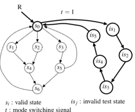
Step 3.1: SynthesizingI SG
We synthesize a combinational logic called an in- valid test state generator(I SG) that can generate all invalid test states as follows. First, we gener- ate an FSM that can traverse all invalid test states from the reset state of the given FSM (see Fig- ure 4). The traversing order and the input val-
is1
is2
is3 is5
is4
t 1
si: valid state isj: invalid test state t: mode switching signal
s1 s2 s3
s4 s5
s6 s0 R
Figure 4: An FSM traversing invalid test states.
ues causing these transitions can be determined arbitrarily. We can achieve complete fault effi- ciency despite of them while the amount of hard- ware overhead depends on them. Then, theI SG is synthesized from the generated FSM. Notice that, the state assignment of these invalid test states is already determined at Step 1 and Step 2.
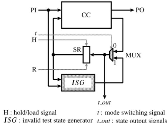
Step 3.2: AppendingI SG
TheI SGgenerated above is appended to the se- quential circuit synthesized at Step 1 with a mul- tiplexer (MUX), a mode switching signal t and state output signals t out (Figure 5). The mode switching signal t controls the MUX and is set to one only when an invalid test state must be set to the SR during test. The state output signals t out is used to observe the responses of test patterns. The SR of the sequential circuit can represent 2n(n: the number of FFs of the SR) states. The number of invalid test states is at most the number of test patterns. It is conceiv- able that the number of invalid test states is much smaller than that of states represented by the SR. Thus we expect that the test application time does not become long and the hardware overhead caused by the extra logic is not high. The transitions to invalid test states are used only during test application. Therefore, we can append the extra logic to the synthesized sequential circuit without changing the combinational logic block.
Step 4: Adding hold mode to the state register
Finally, we add hold mode to the SR. This hold mode is utilized to reduce test application time. We give the details in Section 5.
While we assume a controller is given as an FSM, this assumption makes no restriction on controllers under con- sideration. Even in the case that a controller is given as a gate-level circuit, this method can be applied by extracting an FSM from the circuit using a state machine extraction algorithm (e.g. one available in SIS[4]).
PI CC PO
SR
t out t
H
R
I SG
t: mode switching signal t out: state output signals H : hold/load signal
I SG: invalid test state generator
MUX 0 1
Figure 5: A controller augmented with an invalid test state generator.
4.2. Delay overhead
For a sequential circuit (a controller), the proposed DFT method appends an MUX in front of the SR and add hold mode to the SR. Thus, a delay overhead is caused at nor- mal operation of the controller due to the MUX and an extra logic for hold mode of the SR. However, the delay overhead is the same as the full-scan DFT method. Moreover, con- trollers can be designed and synthesized with taking the de- lay overhead into consideration because the delay overhead can be estimated at the first step of designing controllers.
On the other hand, anI SGgives no affect to the normal operation of a controller. If we can synthesize theI SGwith shorter delay than the combinational logic block, we can perform test application at the normal operation speed.
4.3. Area overhead
For a sequential circuit (a controller), the proposed DFT method has an area overhead due to the I SG, the MUX, and an extra logic for hold mode of the SR. The areas of the MUX and the extra logic are the same as that of the full- scan DFT method. This method appends theI SG which generates the invalid test states to the sequential circuit. The order of the invalid test states generated by theI SG does not affect fault efficiency. However, it is conceivable that the order affects the area of theI SG. Therefore, we can minimize the area overhead by considering the appropriate order of the invalid test states.
If we design a sequential circuit as shown in Figure 6, we can control the values of some FFs in the SR directly from primary inputs. In this case, only the values of the FFs which can not be controlled directly from primary inputs have to be generated by theI SG, and thus, the number of invalid states generated by theI SGare reduced. Therefore, the area of theI SGcan be reduced.
PI CC PO
SR
t out t
H
R
I SG MUX
1 00
1
Figure 6: An example of invalid test state generation using primary inputs.
4.4. Observation points
We suppose that t out shown in Figures 5 and 6 is an observation point for testing. Thus primary output pins for t outare required. However, due to limitation of the number of primary output pins, we may not use sufficient primary output pins for t out. An RTL circuit generally consists of a controller and a datapath. When testing the controller, the datapath is not used. Hence we can use the primary output pins of the datapath as the observation points of the con- troller. Thus, t out can be observed at the primary output pins of the datapath by inserting an extra MUX in front of the primary output pins. In the case when the datapath does not have sufficient primary output pins, we can observe a parity of t out using an XOR tree. If an error of a fault is observed at an odd number of t out, the fault can be de- tected. If an error of a fault is observed at an even number of t out, the fault can not be detected. Fujiwara et al.[5] show that, for most faults, an error of a fault is observed at an odd number of outputs by experiments with ISCAS’89 benchmarks.
5. Test Application Method
In this section, we propose a test application method cor- responding to the proposed non-scan DFT method for con- trollers. Here, we only discuss application of test patterns because we assume that responses of test patterns can be observed as mentioned above.
5.1. Applying valid test patterns
Each valid test pattern can be applied to a sequential cir- cuit using normal operation of the sequential circuit as fol- lows.
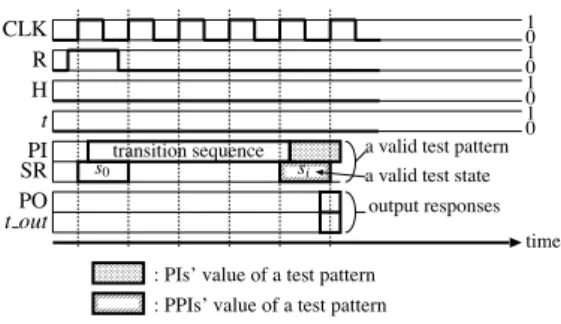
Step 1: Applying PPI value of a test pattern
First, we find a transition sequence from the reset state to the valid test state corresponding to the PPI value of the test pattern. Then, we set the valid test state to the
: PIs’ value of a test pattern : PPIs’ value of a test pattern PI
SR PO t R H CLK
t out
time 10 10 10 10 transition sequence
output responses a valid test pattern a valid test state
s0 si
Figure 7: Applying valid test patterns.
SR (see Figure 7) by applying the transition sequence under the normal operation mode (the mode switching signal t 0).
Notice that, if the combinational logic block contains a fault, we may not set the valid test state to the SR. However, the fault can be detected during the above step because the value loaded into the SR can be observed from t out. Step 2: Applying PI value of a test pattern
We apply the PI value of the test pattern to the primary inputs of the sequential circuit (see Figure 7). For a valid test state, there may exist two or more valid test patterns which contain the valid test state. Therefore, the length of the test sequence can be reduced if we apply the PI values of the test patterns one after another with hold- ing the PPI value at the SR (see Figure 8).
Moreover, a valid test state sjmay be reached from an- other valid test state siby transitions of the normal operation without reset. Therefore, we can reduce the length of a test sequence if we can set sj to the SR using the transitions without reset (see Figure 8). Notice that, in this case, we have to hold the state si in the SR for one more cycle af- ter applying all test patterns that contain the state sias (2) in Figure 8. Hence a transition sequence which starts from the reset state and traverses all valid test states can set all PPI values to the SR. We call such a transition sequence a valid test state traversing sequence. Here, there always ex- ists such a valid test state traversing sequence because any valid test state is reachable from the reset state and the reset state can be reached from any state using the reset signal. Let Lvtand Nvpbe the length of a valid test state traversing sequence and the number of valid test patterns, respectively. The length of a test sequence required to apply all valid test patterns is Lvt Nvp.
We can obtain the shortest test sequence required to ap- ply all valid test patterns, if we obtain the shortest valid test state traversing sequence. We can obtain the shortest valid test state traversing sequence by solving the traveling salesman problem (TSP)[6] at a directed graph where nodes are all valid test states and the weight between nodes is the length of the shortest transition sequence between the two states. Although TSP is an NP-hard problem, we can ob-
10 10 10 10
PI trans.
SR PO t R H CLK
t out
time
s0 si sj
trans.
(1) (2)
Figure 8: Applying valid test patterns using hold mode of state register.
PO t R H CLK
t out
10 10 10 10
time
s0 is1 is2 is3 is4
PI SR
Figure 9: Applying invalid test patterns.
tain the shortest (or may be nearly shortest) valid test state traversing sequence using existing heuristic algorithms for TSP.
Notice that, time required to solve TSP is much shorter than the total test generation time of our method because the number of states of the FSM is generally much smaller than that of gates of the test generation model of the sequential circuit synthesized from the FSM.
5.2. Applying invalid test patterns
Each of invalid test patterns can be applied in the same way as valid test patterns using theI SG (invalid test state generator). In the rest of this paper, for simplicity, we as- sume that primary inputs are not used as inputs of theI SG. The transition modes are switched as shown in the timing chart of Figure 9.
The length of the shortest invalid state transition se- quence (included applying reset signal at the beginning) is the number of invalid test states plus 1 because the I SG generates all invalid test states in turn. Therefore, letting Nis and Nipbe the numbers of invalid test states and invalid test patterns, respectively, the length of a test sequence required to apply all invalid test patterns is Nis Nip 1. In the worst case, the length of the test sequence is only Nip 2 1.
5.3. Testing of extra logic
Appended logic circuits in the DFT process are anI SG and an MUX added in front of the SR. Since theI SG is not used at the normal operation, we test theI SGonly to confirm that the invalid test states are generated correctly.
It is performed by observing state output signals t out at in- valid test pattern application, simultaneously. Testing of the MUX is performed as follows. Since appending the MUX in front of SR is known beforehand, we can generate test patterns for a combinational test generation model includ- ing the MUX.
6. Advantage of Our Method
In this section, we compare our DFT method with the full-scan DFT method[1] and Patel’s non-scan DFT method[3] in test generation time, fault efficiency, test ap- plication time and area overhead. Then we present the re- sults of experiments.
6.1. The full-scan DFT method
Given a sequential circuit, the full-scan DFT method guarantees complete fault efficiency and can generate a test sequence with short test generation time because a test gen- eration model of the sequential circuit is a combinational circuit. However, the method requires scan in/out opera- tions for applying and observing test patterns, and thus it requires extremely long test application time. Letting AMUX and NFFbe the area of a MUX (two one bit inputs and one bit output) and the number of FFs, respectively, the area overhead of the method is NFF AMUXbecause each FF of the SR is replaced with a scannable FF. Letting Npatbe the number of test patterns, the test application time required to apply all test patterns and to observe the responses is Npat NFF 1 NFF. Therefore, if the number of FFs of the SR is larger, the test application time is longer.
This method does not allow at-speed test application be- cause the speed of scan sifting operation is slower than the normal operation speed.
6.2. Patel’s non-scan DFT method
Given a sequential circuit, Patel’s non-scan DFT method appends an MUX to control the values of some FFs in the SR directly from primary inputs. The controllable FFs are selected to cut feedback loops except self loops and to max- imize controllability. The observability of the circuit is im- proved by inserting observation points which are connected to an XOR tree circuit with a primary output.
If the number of primary inputs is equal to or larger than that of FFs in the sequential circuit, all FFs can be controlled directly from the primary inputs, and thus this method can guarantee complete fault efficiency and can generate a test sequence with short test generation time because the test generation model is a combinational circuit. In this case, the area overhead is NFF AMUX. In order to apply each of test patterns, two system clock cycles are required because the value of the SR is set through primary inputs. The test
application time required to apply all test patterns and to observe the responses is Npat 2 1 cycles.
On the other hand, if the number of primary inputs is smaller than that of FFs in the sequential circuit, this method can not guarantee complete fault efficiency and re- quires long test generation time generally because the test generation model is a sequential circuit. Moreover, the gen- erated test sequence tends to become longer because the se- quence contains initialization sequences of FFs which are not controlled directly from primary inputs. In this case, letting NPIbe the number of primary inputs, the area over- head is NPI AMUX. Letting Lseqbe the length of obtained test sequence, the test application time required to apply all test patterns and to observe the responses is Lseq 2 1 cycles.
In this method, at-speed test application can be per- formed.
6.3. Our method
Given a sequential circuit, our non-scan DFT method can guarantee complete fault efficiency. Test generation of our method for a controller consists of generating test patterns for the test generation model and obtaining a valid test state traversing sequence of the FSM. Test sequence for the controller is constructed from these test patterns using the valid test state traversing sequence. Those test patterns can be generated with short test generation time because the test generation model is a combinational circuit. Notice that, time required to obtain the valid test state traversing sequence is negligible compared to the combinational test generation time. Letting AI SG be the area of theI SG, the area overhead is NFF AMUX AI SG. TheI SGis a com- binational logic which generates only invalid test states. In Section 6.4, we evaluate the area with experiments using FSM benchmarks. Letting Lvt and Nis be the length of a valid test state traversing sequence and the number of in- valid test states, respectively, the test application time re- quired to apply all test patterns and to observe the responses is Lvt Nis Npat 2 cycles.
In this method, at-speed test application can also be per- formed.
6.4. Experimental Results
We show experimental results with MCNC’91 FSM benchmark set[7]. The benchmark characteristics and re- sults of logic synthesis are shown in Table 1. In our experi- ment, we used a logic synthesis tool AutoLogic II (Mentor- Graphics) with sample libraries of MentorGraphics on S- 4/20 model 712 (Fujitsu) workstation. Columns “circuit”,
“#states”, “#PIs” and “#POs” denote FSM name, the num- ber of states, the number of primary inputs and the number of primary outputs of original FSMs, respectively. Columns
Table 1: FSM benchmark characteristics and areas af- ter logic synthesis.
circuit #states #PIs #POs #FFs area (gates)
bbara 10 4 2 4 410.30
bbsse 16 7 7 4 781.20
bbtas 6 2 2 3 87.60
beecount 7 3 4 3 331.50
dk14 7 3 5 3 295.10
dk16 27 2 3 5 510.40
dk27 7 1 2 3 92.00
dk512 15 1 3 4 220.80
ex1 20 9 19 5 2740.50
ex2 19 2 2 5 416.90
ex3 10 2 2 4 192.80
ex4 14 6 9 4 479.20
ex5 9 2 2 4 183.70
ex7 10 2 2 4 189.60
keyb 19 7 2 5 1835.40
lion9 9 2 1 4 322.10
opus 10 5 6 4 567.60
planet1 48 7 19 6 2791.10
planet 48 7 19 6 2791.10
pma 24 8 8 5 1068.60
s1488 48 8 19 6 6190.20
s1494 48 8 19 6 6242.80
s1 20 8 6 5 2396.00
s208 18 11 2 5 2361.30
s27 6 4 1 3 416.30
s298 218 3 6 8 8720.80
s386 13 7 7 4 1241.10
s420 18 19 2 5 2217.50
s510 47 19 7 6 1184.20
s820 25 18 19 5 4411.00
s832 25 18 19 5 4543.70
sse 16 7 7 4 781.20
styr 30 9 10 5 2748.90
tma 20 7 6 5 802.70
train11 11 2 1 4 364.50
“#FFs” and “area” denote the number of FFs and circuit ar- eas after synthesis, respectively. Here, areas are estimated using gate equivalent of the library cell area.
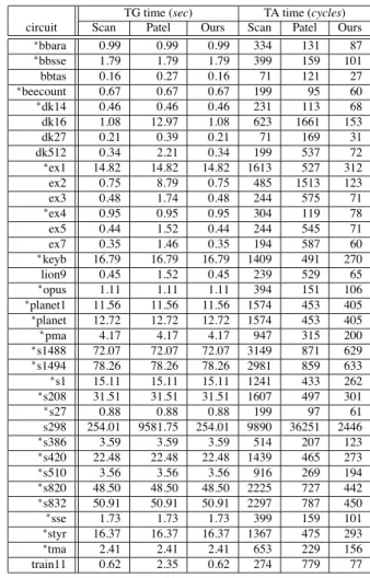
Table 2 shows test generation results of each method. We used a combinational/sequential test generation tool Test- Gen (Sunrise) on the workstation. Columns “Scan”, “Pa- tel” and “Ours” in column “TG time” denote test generation time in seconds of the full-scan method, Patel’s method and our method, respectively. Similarly, column “TA time” de- notes test application time in cycles.
Test generation time of the proposed method is the same as that of the full-scan DFT method because test patterns are generated for the same combinational test generation model. In the column “circuit”, symbol “ ” denotes that the number of primary inputs is larger than or equal to the number of FFs. In Patel’s method, the combinational test generation algorithm can also be applied to these circuits. Thus Patel’s method guarantees complete fault efficiency for these circuit. Experimental results show that fault ef-
Table 2: Test generation results of each method.
TG time (sec) TA time (cycles) circuit Scan Patel Ours Scan Patel Ours
bbara 0.99 0.99 0.99 334 131 87
bbsse 1.79 1.79 1.79 399 159 101
bbtas 0.16 0.27 0.16 71 121 27
beecount 0.67 0.67 0.67 199 95 60
dk14 0.46 0.46 0.46 231 113 68
dk16 1.08 12.97 1.08 623 1661 153
dk27 0.21 0.39 0.21 71 169 31
dk512 0.34 2.21 0.34 199 537 72
ex1 14.82 14.82 14.82 1613 527 312
ex2 0.75 8.79 0.75 485 1513 123
ex3 0.48 1.74 0.48 244 575 71
ex4 0.95 0.95 0.95 304 119 78
ex5 0.44 1.52 0.44 244 545 71
ex7 0.35 1.46 0.35 194 587 60
keyb 16.79 16.79 16.79 1409 491 270
lion9 0.45 1.52 0.45 239 529 65
opus 1.11 1.11 1.11 394 151 106
planet1 11.56 11.56 11.56 1574 453 405
planet 12.72 12.72 12.72 1574 453 405
pma 4.17 4.17 4.17 947 315 200
s1488 72.07 72.07 72.07 3149 871 629
s1494 78.26 78.26 78.26 2981 859 633
s1 15.11 15.11 15.11 1241 433 262
s208 31.51 31.51 31.51 1607 497 301
s27 0.88 0.88 0.88 199 97 61
s298 254.01 9581.75 254.01 9890 36251 2446
s386 3.59 3.59 3.59 514 207 123
s420 22.48 22.48 22.48 1439 465 273
s510 3.56 3.56 3.56 916 269 194
s820 48.50 48.50 48.50 2225 727 442
s832 50.91 50.91 50.91 2297 787 450
sse 1.73 1.73 1.73 399 159 101
styr 16.37 16.37 16.37 1367 475 293
tma 2.41 2.41 2.41 653 229 156
train11 0.62 2.35 0.62 274 779 77
ficiency of s298 is 99.55% and other circuits are 100% in Patel’s method. The full-scan method and our method guar- antee complete fault efficiency for all circuits.
Test application time of the full-scan and Patel’s methods are calculated from the formulas mentioned in Sections 6.1 and 6.2, respectively. Test application time of our method is calculated from the formula mentioned in Section 6.3. In order to obtain a valid test state traversing sequence, we implemented a simple algorithm to solve the TSP. In our method, for all circuits, the length of each test sequence is shorter than other two methods. Particularly, in s298, the ratio of our method to the full-scan method is one to four and of our method to Patel’s method is one to fifteen. If a more efficient algorithm is used to solve the TSP, the test application time of our method may become shorter.
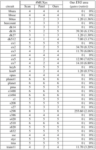
Table 3 shows area overheads of each method. Columns
“Scan”, “Patel” and “Ours” in column “#MUXes” denote the number of MUXes of each method. The MUXes over- head of our method is equal to the full-scan method and is generally larger than Patel’s method. Column “Our I SG
Table 3: Area overheads of each method.
#MUXes OurI SGarea
circuit Scan Patel Ours (gates (ratio))
bbara 4 4 4 0 ( 0%)
bbsse 4 4 4 0 ( 0%)
bbtas 3 2 3 1.20 (1.36%)
beecount 3 3 3 0 ( 0%)
dk14 3 3 3 0 ( 0%)
dk16 5 2 5 39.30 (6.13%)
dk27 3 1 3 1.20 (1.30%)
dk512 4 1 4 7.00 (3.17%)
ex1 5 5 5 0 ( 0%)
ex2 5 2 5 34.70 (8.32%)
ex3 4 2 4 11.70 (6.06%)
ex4 4 4 4 0 ( 0%)
ex5 4 2 4 12.90 (7.02%)
ex7 4 2 4 14.10 (6.80%)
keyb 5 5 5 0 ( 0%)
lion9 4 2 4 1.20 (0.37%)
opus 4 4 4 0 ( 0%)
planet1 6 6 6 0 ( 0%)
planet 6 6 6 0 ( 0%)
pma 5 5 5 0 ( 0%)
s1488 6 6 6 0 ( 0%)
s1494 6 6 6 0 ( 0%)
s1 5 5 5 0 ( 0%)
s208 5 5 5 0 ( 0%)
s27 3 3 3 0 ( 0%)
s298 8 3 8 255.60 (2.16%)
s386 4 4 4 0 ( 0%)
s420 5 5 5 0 ( 0%)
s510 6 6 6 0 ( 0%)
s820 5 5 5 0 ( 0%)
s832 5 5 5 0 ( 0%)
sse 4 4 4 0 ( 0%)
styr 5 5 5 0 ( 0%)
tma 5 5 5 0 ( 0%)
train11 4 2 4 11.70 (3.20%)
area” denotes I SG area overhead in gate equivalent and percentage of the area for the corresponding controller. Here, each I SG was synthesized as Figure 6. Although the order of generating valid test states affect the area of the I SG, in this experiments, we determined simply the order. Area overheads of circuits with “ ” in Table 2 are all zero because these circuits do not requireI SGs. The average of I SG area overhead over the circuits requiringI SGs (ex- cluding the circuits with “ ”) is only 3.5%. The smallest overhead is 0.37% and the largest is only 8.32%. TheI SG area overhead can be more reduced as mentioned in Section 4.3.
Experimental results show that the proposed method guarantees complete fault efficiency and generates test pat- terns with short test generation time. Although some bench- marks requireI SGs, theI SGarea overhead is very small (the average of the area overhead is only 3.5%). More- over, we also show that test application time of the proposed method is shorter than other two methods for all bench- marks.
7. Conclusion
Although the full-scan DFT method can achieve com- plete fault efficiency with short test generation time, it needs extremely long test application time. Moreover, it does not allow at-speed test application. Although Patel’s non-scan DFT method allows at-speed test application, it is not guar- anteed to achieve complete fault efficiency with short test generation time.
In this paper, we proposed a new DFT method for con- trollers to achieve complete fault efficiency with short test generation time. The DFT method allows at-speed test ap- plication. We also proposed a test application method cor- responding to the DFT method. Experimental results show that the test application time of the proposed method is shorter than that of previous methods for all FSM bench- marks. The average area overhead ofI SGis only 3.5% for FSM benchmarks which requireI SGs to be appended. Acknowledgments The authors would like to thanks Drs. Tomoo Inoue and Michiko Inoue of Nara Institute of Science and Technology for their valuable discussions. This work was supported in part by Semiconductor Technology Academic Research Center (STARC) under the Research Project.
References
[1] H. Fujiwara: Logic Testing and Design for Testability, The MIT Press, 1985.
[2] P. C. Maxwell, R. C. Aitken, V. Johansen and I. Chiang: “The effect of different test sets on quality level prediction: when is 80% better than 90%?,” in Proc. of International Test Confer- ence, pp. 358–364, 1991.
[3] V. Chickermane, E. M. Rudnick, P. Banerjee and J. H. Patel:
“Non-scan design-for-testability techniques for sequential cir- cuits,” in Proc. of 30th ACM/IEEE Design Automation Con- ference, pp. 236–241, 1993.
[4] E. M. Sentovich et al.: “SIS: A system for sequential circuit synthesis,” Technical Report UCB/ERL-M92/41, University of California, Berkeley, 1992.
[5] H. Fujiwara and A. Yamamoto: “Parity-scan design to reduce the cost of test application,” IEEE Transaction on Computer- Aided-Design, Vol. 12, No. 10, pp. 1604–1611, 1993. [6] M. R. Garey and D. S. Johnson: Computer and Intractability,
W. H. Freeman and Company, 1979.
[7] S. Yang: “Logic synthesis and optimization benchmarks user guide,” Technical Report 1991-IWLS-UG-Saeyang, Micro- electronics Center of North Carolina, 1991.
[8] H. Wada, T. Masuzawa, K. K. Saluja and H. Fujiwara: “A non-scan DFT method for RTL data paths to provide complete fault efficiency (in Japanese),” Technical Report VLD97–79, IEICE, 1997.