Bidirectional Delay Test of FPGA Routing Networks
Elena Hammari
1, Michiko Inoue
2, Einar J. Aas
1, Hideo Fujiwara
21
Norwegian University of Science and Technology, 7491 Trondheim, Norway
2
Nara Institute of Science and Technology, Kansai Science City, 630-0192, Japan
E-mail: {elena.hammari, einar.j.aas}@iet.ntnu.no, {kounoe, fujiwara}@is.naist.jp
Abstract
This paper documents a novel test method for detection of small delay faults in FPGA routing networks. Such delays may be caused by resistive open defects, which are considered to be major contributions to test escapes.
According to previous research the form of a test path affects the capability of fault detection. In this work, detection accuracy is defined, calculated and measured in SPICE for test paths with different lengths and number of fan-outs. It is shown that the accuracy of detection depends on the defect site relative to the point of test pattern application.
Based on the results of the evaluation, test configurations are developed that exercise the routing network of FPGA by short branched test paths, and a test procedure is proposed where test patterns are applied to both ends of all bidirectional segments.
Comparison with previous test methods shows that the proposed method is more accurate, while keeping the number of test configurations. More test configurations yield improved detection accuracy.
Keywords
FPGA interconnect testing, delay testing, resistive open defects, branch-adding technique
1. Introduction
A Field Programmable Gate Array (FPGA) is being used in a wide range of commercial applications. The main trend in FPGA development has been to increase operating frequency and increase the number of programmable resources, while reducing transistor sizes. However, FPGAs with small and tightly packed transistors are more vulnerable to defects in the fabrication process. Small defects induce increased delays that may fail FPGAs at higher frequencies. In [1] it was reported that resistive open defects, i.e. partial opens, in vias between each layer are the major type of defects escaping tests.
To assure that FPGA operates correctly at higher frequencies, several tests have been proposed to detect small defects [2], [3], [4]. These works target defects in the routing network of FPGAs since routing occupies typically 80% of the FPGA area [5].
The common approach is to check the delay of the segment under test relative to the delay of the fault-free segment. The test clock period must allow small delay defects on the segment due to process variation. This acceptable delay margin determines the smallest delay fault that can be detected by the test. [2] introduced relative delay measurement by comparing delays of identically configured test paths. For absolute delay measurement, [3] pointed out that delay margin decreases with the length of the test path, and suggested using short test paths. [4] observed that delay increase in segments with resistive open defects can be boosted by adding extra branches to the test path, and proposed a test utilizing branched test paths. However, only accuracy of defects located in a stem of a test path was considered.
In this paper, the branch-adding technique is developed further through examination of detection accuracy in the branches of a test path. Detection accuracy is defined as the smallest defect size that can be detected. Subsequently, a test is proposed, where all segments outside switch matrices are tested by test path stems, and segments inside switch matrices are tested in both directions. The main contribution is a trade-off between detection accuracy and test application time.
This paper is organized as follows. Section 2 gives the theoretical background for the delay testing of FPGA. Section 3 defines detection accuracy and shows how it is calculated for different defect locations. Section 4 presents measured detection accuracies from SPICE simulation on an FPGA interconnect model. Section 5 describes the proposed test method, which is evaluated in Section 6. Finally, Section 7 concludes the paper.
2. Model of FPGA routing network
2.1 FPGA architecture13th IEEE European Test Symposium (ETS'08), May, 2008.
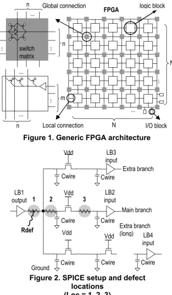
Figure 1 illustrates the generic FPGA architecture used in this paper. It is a symmetrical island-style SRAM FPGA, and employs an NxN array of logic blocks interconnected by a routing network. On the periphery, the array is boarded by input/output blocks. The function of each logic block and connection in the routing network is selected by configuring SRAM memory cells. The routing network consists of global and local routing resources. The global resources are comprised of parallel wiring channels in the horizontal and vertical directions consisting of lines interconnected by programmable switch matrices. The channel width between neighboring switch matrices is n lines.
The local routing resources connect logic blocks to the line segments in the channels. They include m lines at each side of a logic block and programmable connectors.
All programmable connections are realized by pass transistors controlled by SRAM cells. Any path from a logic block output to a logic block input emanates from an output buffer, passes through some pass transistors and ends at an input buffer. The shortest reconfigurable path passes through one pass transistor. A fan-out can be added to the path either at the local connectors or in the switch matrices. The maximum fan-out in a switch matrix is 3 branches.
The functionality of the logic block is used for test generation and propagation of test responses. Flip-flops apply test patterns to the test path, and capture test responses. Look-Up Tables (LUTs) configured as AND/OR gates combine test responses from several test paths.
The basic idea for delay fault testing given here is applicable to more advanced architectures as well, e.g. Virtex or Stratix.; as long as they employ several combinational logic blocks, and are interconnected by switch matrices.
2.2 Delay fault testing
The objective of delay testing is to detect delay faults, and ensure that the design meets the desired performance specifications. Delay faults are activated and observed by propagating signal transitions through the circuit [6]. If a signal transition doesn’t appear at the output in time, a delay fault is detected on the tested path. Two signal transitions are required: low-to-high and high-to low.
When circuits are designed, they have a delay margin, allowing for signals having small delay variations due to process variations. Delay margin is the allowable increase of the propagation time of a signal above the nominal value. A typical delay value margin is 10 % [3]. We used this value in our calculations and simulations.
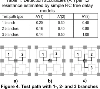
2.4 A model of FPGA interconnect
In our simulations we used a model of FPGA interconnect similar to [4], shown on Figure 2. The connection between two neighboring logic blocks (LBs) is modeled as a line that goes through a pass transistor and connects two buffers. The pass transistor may be the transistor in a local connection, or in a switch matrix. Extra branches are added by switching on other pass transistors in the same local connection or switch matrix.
We assumed zero wire resistance and modelled wire capacitance separately for each segment, to be able to measure propagation delays more accurately. Capacitor Cwire represents total capacitance in each segment. The same capacitance value was used for all segments, and all transistors were chosen to have equal sizes.
Local connection n
m
FPGA
... switch matrix
. . .
... ...
...
. . . . . .
N
N
I/O block . . .
n
n
Global connection logic block
Figure 1. Generic FPGA architecture
Cwire Cwire
Cwire Cwire
Cwire
Cwire Cwire
1
Extra branch
Rdef
2 3
LB2 input LB1
output
Vdd
LB4 input LB3
input
Vdd
Vdd Vdd
Main branch
Ground
Extra branch (long)
Figure 2. SPICE setup and defect locations
(Loc = 1, 2, 3)
Resistive open defects were inserted as extra resistors, one at a time, to three different locations: (1) – at the output of LB1, in the beginning, or stem, of a test path; (2) – in the branch of the test path just after the fan-out point, (3) – in the branch of the test path at the input to LB2 or LB4.
3. Detection accuracy
3.1 Definition of detection accuracy
In this paper, detection accuracy A of a test path is defined as the smallest resistive defect size RDEF that can be detected by the path. Let T(RDEF, loc), TM and TDO be delay of the test path with defect of size RDEF at a location loc, the delay margin of the test path and the delay of the fault-free path, respectively. The delay fault is detected if the delay ratio of the faulty path T(RDEF)/TD0 exceeds the delay margin ratio t=TM/TD0. Thus, the detection accuracy A(loc) of the location loc is defined as follows:
0 0
( ) min DEF DEF, D (3.1)
D
T(R loc) T
A loc R t
T
⎧ − ⎫
⎪ ⎪
= ⎨ ≥ ⎬
⎪ ⎪
⎩ ⎭
3.2 Simplified view with RC tree structures
We will first study simplified RC structures. In particular, we will look for locations of highest sensitivity with respect to resistive open defects. We will apply two widely used delay models: the Elmore delay formula [7] and Penfield-Rubinstein-Horowitz theorem [8].
First, let us employ the Elmore delay model [7] of an RC chain, see Figure 3. The delay T from the input to the output of an N-stage RC chain is computed as:
1 1
(3.2)
N k
N k m
k m
τ C R
= =
=
∑ ∑
Consider a 1-branch shortest test path (Figure 4a): the test path goes through three pass transistors – at the output of logic block 1, in a switch matrix and at the input of logic block 2. We replace each transistor by a resistor with the value equal to its on-resistance and model the test path as a 3-stage RC chain (Figure 3). For simplicity, we assume that all resistors are equal, and all capacitors are equal.
We notice that equation (3.2) may be written as:
3 3
( ) ( ) (3.3)
1 1 2 3 2 2 3
T =R C +C +C +R C +C +R C
The sensitivity of any Ri can be studied. We set all capacitances to the same value: Ci =C. Then, after some manipulation, (3.3) may be written as:
(4 ) i i (3.4)
T = −i R C+B
where Ri is any one of the resistances (R1, R2, R3), and Bi is the rest of the terms of (3.3), independent of R i.
If a defective resistance value, δRi, is added to Ri, the corresponding increase in delay is given from (3.4) as:
(4 ) (3.5)
i i
T i R C
δ = − δ
Obviously, δTi / δRi is maximum for i=1. When we consider Figure 3, (3.5) is in conformance with what we expect; a resistance closer to the stem (input) yields a bigger IR drop than those far away from the input, and will influence the delay value most.
Let us simplify more to focus on the effect of a defect RDEF (δRi) at various locations. If every pass transistor is equal, then we can set Ri = R, which yields T = 6RC from (3.3). We may then compute the relative delay increase due to the resistive change δRi from (3.5):
/ ((4 ) / 6) / (3.6)
i i
T T i R R
δ = − δ
We choose the value δTi /T = 0.1 as the delay margin value, as in [3]. Inserted into (3.6), and rearranging, we obtain:
(0.6 /(4 )) / (3.7)
Ri i R
δ = −
This δRi is the detection accuracy defined in (3.1). Obviously, the best sensitivity, i.e. lowest value of Ri
before a delay fault of 10% is observed, will be for i=1; which is closest to the input (or stem).
For the 2-branch and 3-branch test paths (Figure 4b, 4c), we exploit similar RC tree models. The Penfield- Rubinstein-Horowitz theorem is a generalization of the Elmore delay formula, see e.g. [8]. Due to the space limitation, we omit the derivation of the detection
GND C1
R1
GND C2
R2
C3
R3
GND
1 2 3
1 2 1 2
3
1 2
a) b) c)
Figure 4. Test path with 1-, 2- and 3 branches
Figure 3. 3-stage RC chain model of 1-branch test path
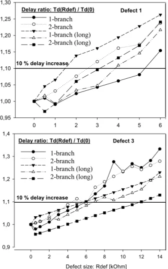
Table 1. Detection accuracies (A*) per Ω resistance estimated by simple RC tree delay
models
Test path type A*(1) A*(2) A*(3)
1 branch 0.20 0.30 0.40
2 branches 0.16 0.40 0.80
3 branches 0.14 0.50 1.00
accuracies for the test paths with 2 and 3 branches. We obtain similar dependency between a Ri and the delay for corresponding test paths. This equation may be written as:
/ ( ) / (3.8)
i i
T T k i R R
δ = δ
where k(i) can readily be found in a similar manner as for (3.6). (3.8) may be used to compute an equation for δRi, the margin for 10% delay increase.
These RC delay models yield the figures in Table 1. We observe that the best detection accuracy (lowest resistive value) is obtained when employing 3 branches with defect location 1. In general, it appears that defect location should appear as close to the test path source (stem) as possible.
In the next section, we will use SPICE simulations to verify that Table 1 in fact shows the correct tendencies of accuracy with respect to defect location and the number of branches activated.
4. SPICE simulations and measurements
We performed SPICE simulation on the interconnect model of Figure 2. During the simulation, low-to-high and high-to-low voltage transitions were applied to the buffer
of LB1 and the delay was measured at the outputs of branch buffers. The detection accuracy was found by adjusting defect resistance until the increase of the delay of the path became equal to the delay margin of 10 %.
Figure 5 and Table 2 show the measured delay ratios and detection accuracies for test paths with 1, 2, and 3 branches. For defects in the stem of the test path (Figure 5, top) it can be seen that adding extra branches increases detection accuracy, in conformity with the results in [4] and our calculations (Table 1). Test path with 3 branches is the most optimal. However adding longer branches gives less increase in delay ratio than adding shorter branches.
For defects in the branches (Figure 5, bottom), detection accuracy decreases as the distance from the fan- out point becomes larger. When the defect is located in 3, the detection accuracy is the lowest. Best detection accuracy is achieved for the test path with 1 branch. This result also supports our calculations (Table 1).
Another interesting observation can be made for the case of 1-branch test path (Table 2): the detection accuracy is the highest for defects located in the beginning of the path. This has a useful consequence. If defects located in the end of a test path can be retested such that they appear in the beginning of a test path, the accuracy of test can be improved. We employ this technique in our novel test presented in the next section.
Note that there is a difference in measured detection accuracies for the low-to-high and high-to-low transitions. It may be caused by the use of equal sizes for p- and n- transistors, or by varying on-resistance in the pass transistors. We are in progress of investigating this.
5. A novel test method
In this section we develop a new test method based on our observations and previous work.
5.1 Accurate test
From previous work we know that short test paths has better detection accuracy than long test paths, and that adding extra branches to a test path increases detection
Table 2. Measured detection accuracies (kΩ)
A(1) A(2) A(3)
Test path type
LH HL LH HL LH HL
1 branch 6 2 6 2 7 6
2 branches 3 2 7 2 7 6
3 branches 2 1 6 2 6 9
LH / HL = low-to-high / high-to-low transition
Defect 3
Defect size: Rdef [kOhm]
0 2 4 6 8 10 12 14
0,9 1,0 1,1 1,2 1,3 1,4
Simple 1 Branch 2 Branches 1 Long Branch 2 Long Branches
10 % delay increase Delay ratio: Td(Rdef) / Td(0)
0 1 2 3 4 5 6
0,95 1,00 1,05 1,10 1,15 1,20 1,25 1,30
Simple 1 Branch 2 Branches 1 Long Br. 2 Long Br.
10 % delay increase
Defect 1 Delay ratio: Td(Rdef) / Td(0)
Figure 5. Delay increase in presence of defects 1-branch
2-branch 1-branch (long) 2-branch (long)
1-branch 2-branch 1-branch (long) 2-branch (long)
accuracy of the stem of the test path. We combine these techniques and use short test paths with 1, 2 or 3 branches to test all segments of the FPGA routing network. The shortest reconfigurable test path starts at the output of a flip-flop in a logic block and ends at the input to a flip-flop in the neighboring block. Each test path goes through one switch matrix, where fan-out can be added. We consider all possible cases for the fan-out in a switch matrix.
Our calculations and simulation showed that in contrast to detection accuracy in the stem of a test path, detection accuracy in the branches becomes worse when extra branches are added. We therefore test all segments outside switch matrices by test path stems.
Segments inside switch matrices cannot be tested by stems of the shortest test paths, as shown on Figure 6. Instead we utilize bidirectional test for this purpose. Our results showed that detection accuracy becomes better when defect location moves towards the point where test pattern is applied (Table 1). By testing switch matrix segments in both directions we ensure that the detection accuracy in this part of the routing network is always close to the detection accuracy of the stem.
Test application time in FPGA is dominated by the time of loading a configuration into FPGA. To reduce the total number of test configurations, as many segments as possible must be tested in the same test configuration.
The detailed steps of how it was done are explained below.
5.2 Test configurations
To find the minimum number of test configurations for each type of test path, first the requirement of
complete test coverage was fulfilled, i.e. the requirement that all segments in
FPGA routing network must be tested. This was done by starting with finding the complete test for the segments inside a switch matrix, separately for the case of 1-branch, 2-branch and 3-branch test paths. Because any test path
goes through a switch matrix, this approach usually gives almost complete test coverage also for the segments outside switch matrices [9] [3] [10].
Next, all switch matrices of the FPGA were identically configured and tthe maximum number of switch matrices that can be tested at the same time was identified. This number was limited by the number of available lines in the routing network of FPGA and represented one test configuration. The procedure was then repeated for the remaining switch matrices and switch matrix configurations until all of them were covered.
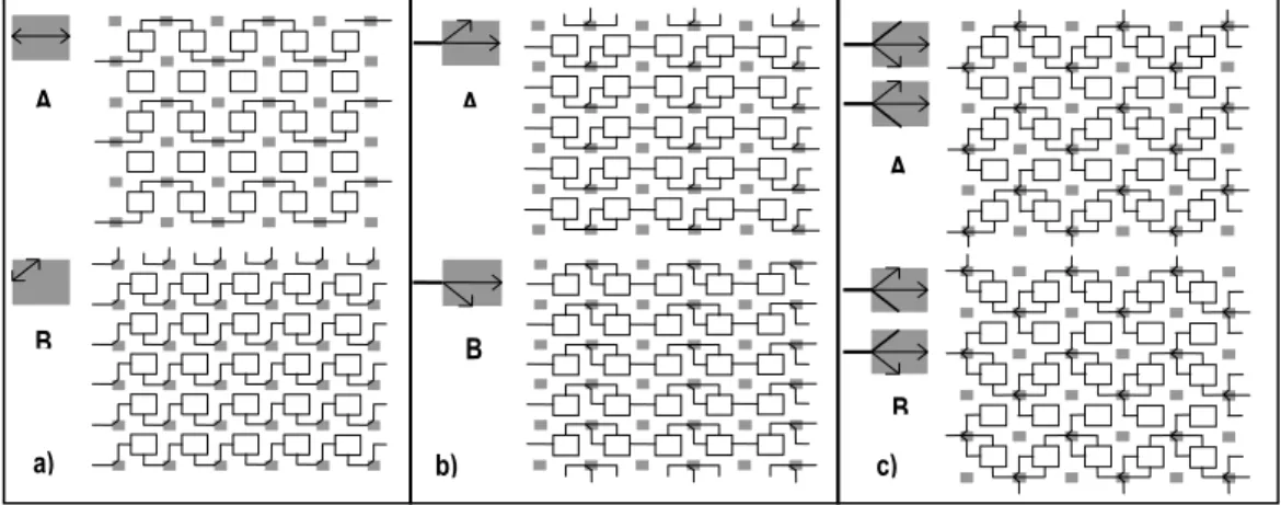
Next, the test was extended to satisfy the requirements of the accurate test (Sec. 5.1). This was done by rotating and mirroring the initial test configurations for the 2- branch and 3-branch test paths. In the case of 1-branch test path, no extra configurations were needed.
Figure 7 shows the resulting test configurations for 1- branch, 2-branch and 3-branch test paths, respectively. Test paths are connected together in chains from primary inputs to primary outputs. Logic blocks combine and forward test responses. Logic blocks with one input implement the identity function. Logic blocks with two inputs implement the AND function during rising delay fault test, and the OR function during falling delay fault
A
B
b) A
B
a)
A
c) B
Figure 7. Test configurations for a) 1-branch test path, b) 2-branch test path, c) 3-branch switch
matrix ...
...
. . .
. . . switch
matrix ... ...
. . . . . .
Tested by branch Tested by branch
Figure 6. Switch matrix test.
All segments are tested by branches of the shortest test paths
test.
In total, 8 test configurations were achieved for the 1- branch case, 32 test configurations for the 2-branch case and 32 test configurations for the 3-branch case. They can be directly derived by shifting and rotating the test configurations on Figure such that all switch matrices and switch matrix directions are covered. The test has 100% segment delay fault coverage.
6. Comparison to previous methods
In this section, the proposed test method is compared to the two previous methods mentioned in the introduction. In the first method [3], all segments of the routing network are tested by 1-branch shortest test paths between two flip-flops. The detection accuracy of the test path is the same as in our test (Table 1). However, in [3] test patterns are applied only in one direction. As a result, around 30 % of the routing network is tested with detection accuracy of defect location 3. In our bidirectional test these parts are tested with detection accuracy of defect location 1, giving an improvement in test accuracy as shown in Table 3.
For complete test of an XC4000 like FPGA architecture having n = 8 global lines and 2 local input lines, the same number of test configurations, 48, are required for both [3] and the proposed method.
In the second method [4] [10], test paths span over 6 switch matrices, and can have 1 or more branches. Using analysis similar to that in Sec. 3.2 we calculated detection accuracies for the test paths with 1-, 2 and 3 branches and compared them to the detection accuracies in the proposed test (Table 1). The results showed that the proposed test is more accurate (Table 4). The improvements come from bidirectional application of test patterns and use of shorter
test paths.
However, the number of test configurations has grown. In [4], 8 test configurations were required to test the whole FPGA for all cases of branched test paths. In the proposed test method 8 test configurations for the 1-branch test path, 32 test configurations for the 2-branch and 3- branch test paths are needed.The gain is the improvements in detection accuracy discussed above, ranging from 33% to 83 %. The real increase in test time is not known until we find the total test time. However, we expect the real increase in test time to be modest. For any particular FPGA, test times can be estimated, and the user may find out whether our method is worth while employing.
7. Conclusion
In this paper a new test method was developed for delay faults in the routing network of an FPGA that targets small resistive open defects. This approach is based on short branched test paths and bidirectional application of test patterns. With the proposed test 30 % of all segments in the routing network can be tested at 66,7 % better detection accuracy compared to the test by short test paths with one-directional application of test patterns. At the cost of four times more test configurations, detection accuracy of the branch-adding technique can be increased by more than 50 % for the 2-branch and 3-branch test paths.
References:
[1] W. Needham, C. Prunty, E. H. Yeoh, High Volume Microprocessor Test Escapes, An Analysis of Defects Our Test are Missing, Proc. Int. Test Conf., pp. 25-34, 1998
[2] E. Chmelar, FPGA Interconnect Delay Fault Testing, Proc. Int. Test Conf., pp. 1239-1247, 2003
[3] Y.-L. Peng, J.-J. Liou, C.-T. Huang, C.-W. Wu, An Application-Independent Delay Testing Methodology for Island- Style FPGA, Proc. of 19th IEEE Int. Symp. on Defect and Fault Tolerance in VLSI Systems, pp. 478-486, 2004
[4] M. B. Tahoori, Testing for Resistive Open Defects in FPGAs, Proc. Field Programmable Technology Conf., pp. 332-335, 2002 [5] M. B. Tahoori, S. Mitra, Interconnect Delay Testing of Designs on Programmable Logic Devices, Proc. Int. Test Conf., pp. 635-644, 2004
[6] K. Angela, C. Kwang-Ting (Tim), Delay Fault Testing, Kluwer Academic Publishers, Boston 1998, pp.44-50
[7] W. C. Elmore. The transient response of damped linear network with particular regard to wideband amplifiers, J. Applied Physics, 19:55–63, 1948.
[8] J. M. Rabaey, Digital Integrated Circuits: A Design Perspective, Prentice-Hall Inc., Upper Saddle River, 1996 [9] M. Renovell, J. M. Portal, J. Figueras, Y. Zorian, Testing the Interconnect of RAM-Based FPGAs, IEEE Design & Test of Computers, pp. 45-50, January-March 1998
[10] M. B. Tahoori, S. Mitra, Automatic Configuration Generation for FPGA Interconnect Testing, Proc. of the 21st IEEE VLSI Test Symp., pp. 134-139, 2003
Table 4. Improvement of detection accuracy
Loc 1 Loc 2 Loc 3
Test path type
A1 (A1-A) /A1 A1
(A1-A) /A1 A1
(A1-A) /A1 1 branch 0,30 33,3 % 0,72 58,3% 3,60 83,3% 2 branch 0,40 60,0% 0,96 58,3% 4,80 83,3% 3 branch 0,48 70,4% 1,16 56,8% 5,80 82,8% A1 = calculated detection accuracy for the test paths in [3]
Table 3. Improvement of detection accuracy
Defect loc. Loc 1 Loc 2 Loc 3
(A0-A)/A0 0 % 0% 66,7%
A0 = calculated detection accuracy for the test path in [2]