Chia Yee Ooi and Hideo Fujiwara Graduate School of Information Science Nara Institute of Science and Technology Kansai Science City, 630-0192 Nara, Japan
{chiaye-o,fujiwara}@is.naist.jp
Abstract—This paper introduces a new class of sequential circuits called acyclically testable sequential circuits which is wider than the class of acyclic sequential circuits but whose test generation complexity is equivalent to that of the acyclic sequential circuits. We also present a test generation procedure for acyclically testable sequential circuits and elaborate a design- for-test (DFT) method to augment an arbitrary sequential circuit into an acyclically testable sequential circuit. Since the class of acyclically testable sequential circuits is larger than the class of acyclic sequential circuits, the DFT method results in lower area overhead than the partial scan method and still achieves complete fault efficiency. Besides, we show through experiment that the proposed method contributes to lower test application time compared to partial scan method. Moreover, the proposed method allows at-speed testing while the partial scan method does not.
Index Terms—Acyclic test generation, design-for-test, sequential circuits, test generation complexity.
I. INTRODUCTION
est generation even for combinational circuits, was shown to be NP-complete almost three decades ago [1]. However, empirical observations tell us that the test generation complexity of practically encountered combinational circuits seems to be polynomial [2]. Based on this observation, several classes of sequential circuits whose test generation complexity is equivalent to combinational test generation complexity have been introduced. These include balanced sequential circuits [3] and internally balanced sequential circuit [4]. In our previous work [5], [6], we introduced τk notation to express the test generation complexity of a given circuit class relatively to the combinational test generation complexity denoted as τ(n)=Θ(nr) where n is the size of the combinational circuit and r is some constant larger than 2. Using time expansion model (TEM) [7], we showed in [5], [6] that the class of acyclic sequential circuits is τ2-bounded, which means the test generation complexity of acyclic sequential circuits is bounded by the square of the combinational test generation complexity, i.e. O(τ2(n)). Therefore, we regard acyclic sequential circuits as easily testable. Thru function has been used in [9] to reduce test generation complexity but the target circuit is datapath only and test generation complexity was not discussed explicitly. [10] also considered existing thru functions in a scan technique but those thru functions are activated by primary inputs only.
In this paper, we introduce a new class of sequential circuits called acyclically testable sequential circuits, which is τ2- bounded. The class of acyclically testable sequential circuits that is defined in this work covers some sequential circuits that are cyclic. The variables that activate a thru function are either primary inputs or registers. In other words, the class of acyclically testable sequential circuits is a proper superset of the class of acyclic sequential circuits. We also present a design-for-test (DFT) method to augment an arbitrary sequential circuit into a circuit that belongs to the class of acyclically testable sequential circuits. We exploit the fact that RTL design information including the existence of thru functions is available early in the design cycle. For a given sequential circuit, our DFT method augments the sequential circuit with thru functions so that the sequential circuit becomes acyclically testable.
The rest of the paper is organized as follows. In Section II, we define R-graph as a representation of sequential circuits and introduce a new concept of testability called acyclic testability. Moreover, we redefine time expansion model (TEM) based on R-graph. In Section III, we discuss the test generation of acyclically testable sequential circuits. In Section IV we present the DFT method to augment an arbitrary sequential circuit into an acyclically testable sequential circuit. Experimental result is presented in Section V and the discussion is concluded in Section VI.
II. PRELIMINARIES
This section introduces a circuit representation called R- graph and the new concept of acyclic testability. We also redefine TEM based on R-graph to facilitate the discussion of test generation model in the following section.
A. R-Graph
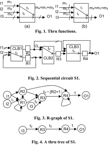
R-graph represents the topology of circuits by grouping flip-flops (FFs) into registers and including the information about thru functions available in the logic. Thru function t is a logic that transfers the signals from the input of the thru function to the output when the thru function is active. Note that the bit width of the input and output are equal. Fig. 1 shows two examples of thru function. Two thru functions are independent if they cannot be active at the same time. t1 and t2
in Fig. 1(b) are independent.
A New Class of Sequential Circuits with Acyclic Test
Generation Complexity
T
1-4244-9707-X/06/$20.00 ©2006 IEEE
24th IEEE International Conference on Computer Design (ICCD'06), pp. 425-431, October 2006.
(a) (b) Fig. 1. Thru functions.
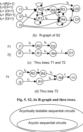
Fig. 2. Sequential circuit S1.
Fig. 3. R-graph of S1.
Fig. 4. A thru tree of S1.
Definition 1: A circuit representation called R-graph is a directed graph GR=(V,A,w,h,t) that has the following properties.
1. Let FFi denote a flip-flop. Let pre(FFi)={FFj | FFj→ c
FFi} (resp. suc(FFi)={FFj | FFi
→
c FFj}) where c is a combinational path. Vertex v∈V is a register, primary input or primary output where each register consists of a maximal set of flip-flops such that pre(FFp)=pre(FFq) and suc(FFp)=suc(FFq) for all FFp, FFq in the set of flip-flops; 2. (vi, vj)∈A denotes an arc if there exists a combinational path from the register corresponding to vi to the register corresponding to vj;3. w:VÆZ+ (the set of positive integers) defines the number of flip-flops in each register corresponding to a vertex;
4. r:VÆ{h, φ} defines the type of register where a register is a hold register if r(v)=h. Else, it is a regular register;
5. t:AÆT∪{φ} (T is a set of thru functions {t0, t1, …, ti}) where t(a)=φ if there is no thru function for a∈A and t(a)≠φ contains the signal values of a set of vertices that activate the thru function, in which each vertex corresponds to a register/flip-flop or PI. If t(a)=1 (identity thru function), the signal values are transferred from the source vertex of arc a to the sink vertex of arc a through a wire logic (not a gate logic) directly without assignment of any signal values.
The hold function of a hold register is regarded to be activated by a primary input in this work.
Example 1: Fig. 3 shows the R-graph of the sequential circuit S1 of Fig. 2. The notation CLB in Fig. 2 means combinational logic block. The thru functions t1—t3, which are the thru functions extracted from the high level netlist of S1, are contained in the R-graph. t3={R2=1} means thru function t3 is activated by signal value 1 at register R2.
In the following text, the vertex that corresponds to a primary input (resp. primary output) is called input vertex (resp. output vertex) while the vertex that corresponds to a register (resp. flip-flop) is called register vertex (resp. flip-flop vertex). Note that the only incoming arc of an output vertex has identity thru function.
B. Acyclic Testability
Prior to the formal definition of the class of ayclically testable sequential circuits, the concept of thru tree is introduced.
Definition 2. Let R-graph GR=(V,A,w,h,t) represent a given sequential circuit S. A thru tree is a subgraph of GR that satisfies the following conditions.
1. It is a rooted tree;
2. There is only one sink (root), which is corresponding to a primary output;
3. The sources are vertices that correspond to primary inputs;
4. All arcs are labeled with a thru function.
In the thru tree, each register is justifiable from a primary input and is observable at a primary output. Fig. 4 shows the only thru tree of the R-graph for S1. A thru function in a thru tree may depend on a signal of another thru tree to become active. Therefore, we introduce a dependency graph for a set of thru trees.
Definition 3. Let GR be the R-graph of a sequential circuit S, and let B be a set of thru trees in GR. The dependency graph of B is a directed graph GD=(VD,AD) such that
1. Vertex v∈VD is a thru tree in B;
2. (vi, vj) ∈AD denotes an arc if there exists a vertex (of GR) in thru tree vi that activates a thru function in thru tree vj.
Definition 4. Let R-graph GR=(V,A,w,h,t) represent a given sequential circuit S. A set of thru trees B in GR is said to be k- consistent with GR if the following conditions are satisfied. 1. The dependency graph of B is acyclic;
2. All thru trees in B are disjoint;
3. Let the maximum depth of thru trees in B be Dmax. Let the maximum length of paths in the dependency graph of B be Lmax. Dmax x Lmax is bounded by k;
4. Any vertex that activates a thru tree Ti in B is either an input vertex or a hold register vertex in B, and activates no other thru tree Tj in B;
5. For each pair of reconvergent paths p1 and p2 that start from u and end at v, there exists a hold register vertex w on p1 but not on p2 such that w is not the second vertex x of p1 and the length of the subpath wÆv of p1 is equal to or longer than the length of any other path pk that starts from w and ends at v if all vertices on p1 and p2 except u, O1
t1
I3
m3
I2
t1
t2
m4=m1=m3
I1 I3 O1
m1
m2
CLB1
t3={R2=1} I1
R1
R3 R4
t2
R2
I2
1
t2
t3 R4 1 I1
CLB2 t1
R3 I3 t2
I2
R1
R2 O1
CLB3 t3
R3 O1 I3
R4 I1
I3 m3 m1
m4=m1+m3
O1 t1
t1
I2 m2
v and x are not included in any thru tree in B and either of the following conditions i and ii is satisfied.
i. p1 and p2 are of equal length and the first arc (u,x) on p1 is labeled with a thru function of a thru tree in B; or ii. p1 is equal to or shorter than p2 and the vertex u
activates the thru function on an arc coming to the vertex x on p1.
Definition 5. A sequential circuit S is said to be k-acyclically testable if the R-graph GR of S contains a set of thru trees B that is k-consistent with GR and covers all the vertices of a feedback vertex set of GR. A sequential circuit S is said to be acyclically testable if S is k-acyclically testable for some constant k.
Example 2: For circuit S1 in Fig. 2, R1 and R4 are the vertices in the minimum feedback vertex set. However, only R4 is contained by the only thru tree in the R-graph as shown in Fig. 4. Therefore, S1 is not acyclically testable.
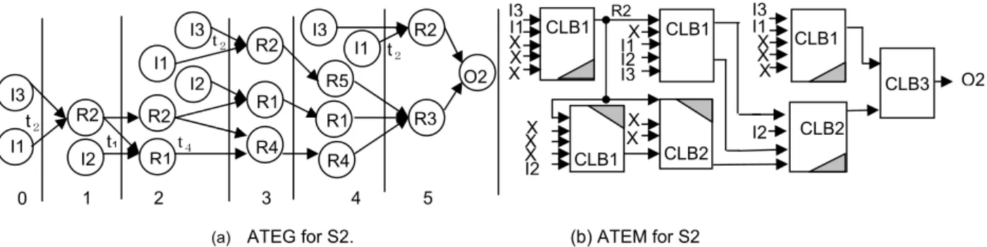
Example 3: Fig. 5(b) shows an R-graph of a sequential circuit called S2 (Fig. 5(a)) whose registers are hold registers. Thru functions t1={R2=1} and t4={R2=1} are activated by R2 and thru functions t2={I3=1}, t3={I3=1} and t5={I3=1} are activated by I3. S2 is an acyclically testable circuit because there are two thru trees, namely T1 and T2 (shown in Fig. 5(c)) that contain R1, R2 and R4, which are the vertices in the minimum feedback vertex set. Although T3 contains all the vertices in the minimum feedback vertex set, the thru tree does not satisfy Condition 1 in Definition 4. Thru functions t1 and t4
are activated by R2, which is also in the same thru tree. In other words, the dependency graph of T3 is cyclic.
An acyclic sequential circuit is an acyclically testable sequential circuit with empty minimum feedback vertex set. In other words, a sequential circuit is acyclically testable if it is acyclic but the converse is not correct. Therefore, we have the following theorem.
Theorem 1. The class of acyclically testable sequential circuits is a proper superset of the class of acyclic sequential circuits (Fig. 6).
(a) Sequential circuit S2
(b) R-graph of S2
T1 T2
(c) Thru trees T1 and T2
T3
(d) Thru tree T3
Fig. 5. S2, its R-graph and thru trees.
Fig. 6. Acyclically testable sequential circuits and acyclic sequential circuits.
C. Time Expansion Model
Time expansion model (TEM) has been introduced in [7], [8] as a test generation model for acyclic sequential circuits based on time expansion graph (TEG). A topology graph is a directed graph of circuit representation where a vertex v denotes a combinational logic block while an arc (u,v) represents a connection from combinational logic block u to combinational logic block v. The authors defined time expansion graph (TEG) for the topology graph of a given acyclic sequential circuit. To facilitate the discussion of test generation model for acyclically testable sequential circuits, we redefine the time expansion graph (TEG) that is used to derive a time expansion model for a given acyclic sequential circuit represented by R-graph.
Definition 6. Let S be an acyclic sequential circuit and let GR=(V,A,w,h,t) be the R-graph of S. Let GT=(VE,AE,T,l) be a directed graph, where VE is a set of vertices, AE is a set of arcs, T is a mapping from VE to a set of integer and l is a mapping from VE to the set of vertices in R. If graph GT satisfies the following five conditions, graph GT is said to be a time- expansion graph (TEG) of GR.
CLB2 CLB1
O2 t4 R3
t4 R4 t3
R1
1 I2 t1
I1 R2
t2
t1={R2=1} I1
R1
R3
O1 R2
t4 1 t2={I3=1}
t3= {I3=1} t4= {R2=1} t5= {I3=1}
t3
t5
R1 R4 1
I2 t1 t4
I1 R2
t2 t5
O2
O1
Acyclic sequential circuits O2
I2 R4
O1
Acyclically testable sequential circuits R5
I3
1
R5 1 t1
t2
I1
R1 O1 t2
t1
t3
I3
t5
R2 R5
R4 I3
CLB3 I2
C1 (Input/Output and register preservation): The mapping l is a surjective, i.e., ∀v∈V,∃u∈VE, s.t. v=l(u).
C2 (Logic preservation): Let u be a vertex in GR. For any direct predecessor v(∈pre(u)) of u in GR, there exists vertices x and w in GT such that l(w)=u, l(x)=v, x∈pre(w) and
|pre(w)|=|pre(u)|.
C3 (Time consistency): For any arc (u,v) (∈AE), there exists an arc (l(u),l(v)) such that T(v)-T(u)=1 if l(u) corresponds to a register or a primary input and l(v) corresponds to a register. T(v)-T(u)=0 if l(u) corresponds to a register and l(v) corresponds to a primary output.
C4 (Time uniqueness): For any pair of vertices u,v (∈VE), if T(u)=T(v) and if l(u)=l(v), then the vertices u and v are identical, i.e., u=v.
C5 (Hold consistency): Let u be a vertex in GT. Let v(∈pre(u)) be a direct predecessor of u. If |pre(u)|<|pre(l(u))| and l(u)=l(v)=w, then r(w)=h and |pre(u)|=1.
Definition 7. Let S be an acyclic sequential circuit. Let GR=(V,A,w,h,t) be the R-graph of S, and let GT=( VE,AE,T,l) be a TEG of GR. The combinational equivalent CE(S) obtained by the following procedure is said to be the time expansion model (TEM) of S based on GT.
1. For each time frame, replace each vertex with a connection without a register and replace each arc with the combinational logic block where the corresponding combinational path (represented by the arc) is located. Each combinational logic block appears at most once at each time frame.
2. A logic gate in each logic block is removed if it is not reachable to any input of other logic blocks.
Example 4: Fig. 7(b) shows the R-graph of one of the acyclic sequential circuit S3 in Fig. 7(a). Its time expansion graph (TEG) and its time expansion model (TEM) are derived in Fig. 7(c) and Fig. 7(d).
(a) Acyclic sequential circuit, S3.
(b) R-graph of an acyclic structure of S3.
0 1 2
(c) Time expansion graph of S3.
(d) Time expansion model (TEM) of S3. Fig. 7. Example of time expansion model.
III. TEST GENERATION MODEL AND PROCEDURE
This section introduces the test generation model called acyclically-extended time expansion model (ATEM) to perform test generation on acyclically testable sequential circuits. The procedure of test generation is also described.
A. Acyclically-Extended Time Expansion Model (ATEM)
An acyclically-extended time expansion model (ATEM) of an acyclically testable circuit is created using its R-graph and its thru trees. We define acyclically-extended time expansion graph (ATEG) and then ATEM. In the following text, pre(u) denotes the set of direct predecessors of u while |pre(u)| denotes the number of all direct predecessors of u.
Definition 8. Let S be an acyclically testable sequential circuit with thru trees B and let GR=(V,A,w,h,t) be the R-graph of S. The acyclically-extended time expansion graph (ATEG) GA=(VA,AA,T,l) with respect to B is a directed graph that satisfies the following conditions.
C1 (Input/Output and register preservation): The mapping l is a surjective, i.e., ∀v∈V,∃u∈VA, s.t. v=l(u).
C2 (Logic preservation for fault excitation): Let u be a vertex in GR. For any direct predecessor v(∈pre(u)) of u in GR, there exists vertices x and w in GA such that l(w)=u, l(x)=v, x∈pre(w) and |pre(w)|=|pre(u)|.
C3 (Thru tree for justification and propagation): Let u be a vertex in a thru tree Ti∈B. Let W⊂pre(u) be a set of all direct predecessors of u in Ti. For each u∈Ti, there exists a vertex v in GA which satisfies the following conditions.
i. l(v)=u;
ii. For each vertex x∈pre(v), the following conditions are satisfied.
a. If there exists a vertex w’ in W such that l(x)=w’ then x∉pre(z) for any z where l(z) is a vertex included in other thru trees except Ti and x∉pre(y) for l(y)=l(x); b. Let Tk be a thru tree that is activated by l(x). If l(x)=l(v),
then |pre(v)|=1 and x∉pre(z) for any z where l(z)≠l(v) and l(z) is a vertex not in thru tree Tk ;
c. If l(x) is a vertex that activates Ti, then x∉pre(z) for any z where l(z)≠l(x) and l(z) is a vertex not in thru tree Ti. C4 (Time consistency): For any arc (u,v) (∈AA), there exists an arc (l(u),l(v)) such that T(v)-T(u)=1 if l(u) corresponds to a register or a primary input and l(v) corresponds to a register. T(v)-T(u)=0 if l(u) corresponds to a register and l(v) corresponds to a primary output.
O1 I1
R2 I3
CLB3 CLB2
CLB1 I3 I1
I2 R1 R2
O1
I2 R1
I1
I3 R2 R1 I1
CLB3
CLB1 CLB2
O1 I3
I1 CLB1 I2
I2 I1
O1
I2
I2
C5 (Time uniqueness): For any pair of vertices u,v (∈VA), if T(u)=T(v) and if l(u)=l(v), then the vertices u and v are identical, i.e., u=v.
C6 (Hold consistency): Let u be a vertex in GA. Let v(∈pre(u)) be a direct predecessor of u. If |pre(u)|<|pre(l(u))| and l(u)=l(v)=w, then r(w)=h and |pre(u)|=1.
C7 (Input Independency): Let u, v be two vertices in GA. Let pi and pj be a pair of reconvergent paths that start from u and end at v. Let w be a vertex on pi such that u∈pre(w). Let x be a vertex on pj such that u∈pre(x). For each pair of paths pi, pj
where w≠x, |pre(w)|=|pre(l(w))| and |pre(x)|=|pre(l(x))|.
Definition 9. Let S be an acyclically testable sequential circuit. The acyclically-extended time expansion model (ATEM) of S is the combinational equivalent obtained by the following procedure.
1. For each time frame, replace each vertex with a connection without a register and replace each arc with the combinational logic block where the corresponding combinational path (represented by the arc) is located. Each combinational logic block appears at most once at each time frame.
2. A logic gate in each logic block is removed if it is not reachable to any input of other logic blocks.
3. Each input that corresponds to an output of a register is assigned don’t care value.
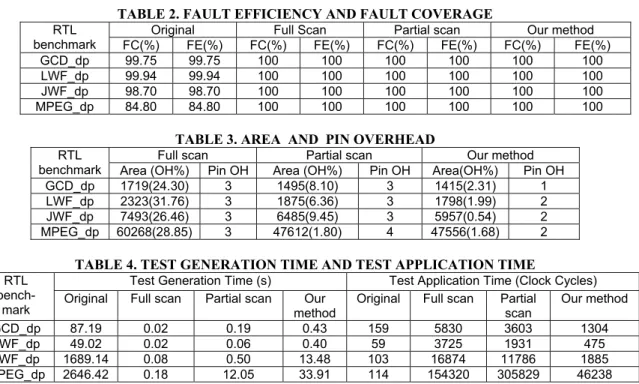
Example 5: For simplicity, Fig. 8 shows the ATEG and ATEM for the subcircuit of S2 which is fan-in cone with output O2. ATEG and ATEM for the whole circuit can be derived similarly. Note that T2 is dependent on T1. Justification of registers R1, R2 and R4 at time 3 is done from time 0 to 3. Note that when R2 of T1 is justified through I1 from time 2 to 3, R1 and R4 of T2 are in hold mode at time 4 (required by c of ii of C3 in Definition 8). R2 of T1 needs to be assigned certain signal value to activate thru functions t1
and t4 but R2 cannot be used for justification and activation simultaneously.
B. Test Generation Procedure
For each stuck-at fault, the test generation process is done as follows using ATEM test generation algorithm. The fault list include faults in thru functions. To guarantee the test generation for faults in thru functions, each register in the feedback vertex set are regarded as having reset function.
Step 1: Generate ATEM of the sequential circuit.
Step 2: Apply combinational ATPG for multiple fault model to the ATEM.
Step 3: Derive the test sequence from the test pattern obtained for the ATEM.
Lemma 1: The ATEM of an acyclically testable sequential circuit is sufficient to generate tests for all testable faults in the circuit.
From Lemma 1, the following theorem is concluded.
Theorem 2: The ATEM test generation algorithm can identify redundancy and all testable faults.
Theorem 3: The test generation complexity of the acyclically testable sequential circuits is τ2–bounded.
Proof: From the definition of ATEM, the number of time frames in the ATEM can extend at most dk + k+ d, where k is at most the total depth of all the thru trees and d is the depth of the acyclic structure of the acyclically testable circuit. By assuming d=O(n), the size of ATEM is (k+1)O(n2)+kO(n) where n is the size of the acyclically testable circuit. Since the test generation is done by applying combinational ATPG on ATEM, the test generation complexity is O(τ2(n)).
IV. DFT METHOD
In this section, a DFT method to augment a given sequential circuit into an acyclically testable sequential circuit is introduced. The DFT method performs some operations on R- graph and it is designed to induce minimum area overhead. The procedure consists of the following three steps.
Step 1: Identify the vertices of minimum feedback vertex set (MFVS).
Step 2: Group the vertices of MFVS into two groups, G1 and G2. One group contains input/output vertices and the vertices that activate a thru function. Another group contains input/output vertices and register vertices that are not in G1. The set of vertices in G1 is disjoint with G2.
Step 3: For each group, build a thru tree by adding minimum new thru functions. Each register is added a reset function if it does not have one.
Step 4: If G1 and G2 have registers, hold function is added to each register. Else, hold function is added to each register that is in neither G1 nor G2. The control input for hold registers in G1 is different from the control input for hold registers in G2.
Example 6: S1 in Fig. 2 is not acyclically testable because R1 and R2 are not contained by any thru tree. By adding new thru functions to arcs (R1,R3) and (R3,R4) that are activated by a new input I4, it becomes acyclically testable. Both R1 and R4 are justifiable from I2 and observable at O1.
V. CASE STUDIES
In the case studies, we conduct experiments on RTL benchmark circuits, which are datapaths of varying bit width. We apply our DFT method on GCD_dp, LWF_dp, JWF_dp, and MPEG_dp and compare the area overhead of the augmented circuits with that of the full scanned circuits and the partial scanned circuits. Partial scanned circuits are the circuits whose minimum feedback set of flip-flops are scanned so that the augmented circuits are acyclic. Thus, the circuits modified with partial scan and with our DFT method have same test generation complexity. Table 1 presents the characteristics of the benchmark circuit. Table 2 shows the fault coverage and fault efficiency of each benchmark circuit. Each fault testable in the partial scan designed circuits is also testable in the corresponding circuit augmented by our DFT method, and vice versa. Table 3 shows the area overhead where one unit of area corresponds to the size of an inverter and pin overhead. It shows that the area overhead of the
benchmark circuits augmented by our method is less than that of the full scanned circuits and the partial scanned circuits. The pin overhead in our method comes from the reset function and extra input to control the new thru functions. Table 4 tells that the test generation time for the original circuits is large while the test generation time for the partial scan designed circuits as well as the acyclically testable sequential circuits is small. Table 5 gives the information that the test application time of the circuits under our augmentation is more than the original circuits’ but less than the partial scan.
VI. CONCLUSION
A new class called acyclically testable sequential circuits has been introduced. The test generation complexity of the acyclically testable sequential circuits is τ2–bounded. On the other hand, acyclically testable sequential circuits are at-speed testable. The DFT method to augment an arbitrary sequential circuit into an acyclically testable sequential circuit has been introduced. Experimental results showed that the area overhead of the resulting augmented circuits is less compared to the partial scan designed circuits. Complete fault efficiency is also achieved and the test generation time is low. Moreover, the test application time is less than the test application time of the full scanned circuits and partial scanned circuits.
ACKNOWLEDGMENTS
This work was supported in part by Japan Society for Promotion of Science (JSPS) under Grants-in-Aid for Scientific Research B(2) (No. 15300018). The authors would like to thank Prof. Tomoo Inoue, Dr. Thomas Clouqueur and
other members of Fujiwara Laboratory who have given their valuable comments.
REFERENCES
[1] P. Goel, “Test generation costs analysis and projections,” Proc. 17th DAC, pp. 77-84, June 1980.
[2] M.R. Prasad, P. Chong, and K. Keutzer, “Why is ATPG easy?” Proc. 36th DAC, pp. 22-28, June 1999.
[3] R. Gupta and M. A. Breuer, “The BALLAST methodology for structured partial scan design,” IEEE Trans. Comput., vol. 39, no. 4, pp. 538-544, April 1990.
[4] H. Fujiwara, “A new class of sequential circuits with combinational test generation complexity,” IEEE Trans. Comput., vol. 49, no. 9, pp. 895-905, Sept. 2000.
[5] C. Y. Ooi and H. Fujiwara, “Classification of sequential circuits based on τk notation,” Proc. IEEE 13th ATS, pp. 348-353, Nov. 2004. [6] C. Y. Ooi, T. Clouqueur and H. Fujiwara, “Classification of sequential circuits based on τk notation and its applications,” IEICE Trans. on Info. and Syst., pp. 2738-2747, Dec. 2005.
[7] T. Inoue, T. Hosokawa, T. Mihara and H. Fujiwara, “An optimal time expansion model based on combinational ATPG for RT level circuits,” IEEE 7th ATS, pp. 190-197, Dec. 1998.
[8] D. K. Das, T. Inoue, S. Chakraborty and H. Fujiwara, “Max- testable class of sequential circuits having combinational test generation complexity,” IEEE the 13th ATS, pp. 342-347, Nov. 2004. [9] H. Iwata, T. Yoneda, S. Ohtake and H. Fujiwara, “A DFT method for RTL data paths based on partially strong testability to guarantee complete fault efficiency,” Proc. IEEE the 14th ATS, pp. 306-311, Dec. 2005.
[10] C. Lin, M. Marek-Sadowska, M.T. Lee and K. Chen, “Cost-free scan: A low-overhead scan path design,” IEEE Trans. CAD Integra. Circuit & Sys., Vol. 17, No. 19, pp. 852-861, Sept. 1998.
(a) ATEG for S2. (b) ATEM for S2
Fig. 8. Test generation model for acyclically testable sequential circuits.
TABLE 1. CHARACTERISTICS Original RTL
benchmark FF Area PI PO
GCD_dp 48 1383 40 19
LWF_dp 80 1763 39 32
JWF_dp 224 5925 106 80
MPEG_dp 1928 46772 499 128
X X X
t1 t4
R2
R3 R5 O2
R1 R4
0 1 2 3 4
I2
R1 I2
R2 I1
R1 R4
I1 I2
I2X X
I1X
O2
X X
t2 t
2
X I2 I1 I3
I3 I3
R2 I1
I3 t2
5 R2
XX
I1X CLB1 CLB1 CLB1
CLB3 CLB2
CLB2 CLB1
R2 I3
I3
TABLE 2. FAULT EFFICIENCY AND FAULT COVERAGE
Original Full Scan Partial scan Our method
RTL
benchmark FC(%) FE(%) FC(%) FE(%) FC(%) FE(%) FC(%) FE(%)
GCD_dp 99.75 99.75 100 100 100 100 100 100
LWF_dp 99.94 99.94 100 100 100 100 100 100
JWF_dp 98.70 98.70 100 100 100 100 100 100
MPEG_dp 84.80 84.80 100 100 100 100 100 100
TABLE 3. AREA AND PIN OVERHEAD
Full scan Partial scan Our method
RTL
benchmark Area (OH%) Pin OH Area (OH%) Pin OH Area(OH%) Pin OH
GCD_dp 1719(24.30) 3 1495(8.10) 3 1415(2.31) 1
LWF_dp 2323(31.76) 3 1875(6.36) 3 1798(1.99) 2
JWF_dp 7493(26.46) 3 6485(9.45) 3 5957(0.54) 2
MPEG_dp 60268(28.85) 3 47612(1.80) 4 47556(1.68) 2
TABLE 4. TEST GENERATION TIME AND TEST APPLICATION TIME
Test Generation Time (s) Test Application Time (Clock Cycles) RTL
bench-
mark Original Full scan Partial scan Our method
Original Full scan Partial scan
Our method
GCD_dp 87.19 0.02 0.19 0.43 159 5830 3603 1304
LWF_dp 49.02 0.02 0.06 0.40 59 3725 1931 475
JWF_dp 1689.14 0.08 0.50 13.48 103 16874 11786 1885
MPEG_dp 2646.42 0.18 12.05 33.91 114 154320 305829 46238