著者
Kondo Takahi r o
j our nal or
publ i c at i on t i t l e
Sc i enc e and t ec hnol ogy of advanc ed m
at er i al s
vol um
e
18
num
ber
1
page r ange
780- 804
year
2017- 10
権利
( C) 2017 The Aut hor ( s ) . Publ i s hed by N
at i onal
I ns t i t ut e f or M
at er i al s Sc i enc e i n par t ner s hi p
w
i t h Tayl or &
Fr anc i s .
Thi s i s an O
pen Ac c es s ar t i c l e di s t r i but ed
under t he t er m
s of t he Cr eat i ve Com
m
ons
At t r i but i on Li c ens e
( ht t p: / / c r eat i vec om
m
ons . or g/ l i c ens es / by/ 4. 0/ ) ,
w
hi c h per m
i t s unr es t r i c t ed us e, di s t r i but i on,
and r epr oduc t i on i n any m
edi um
, pr ovi ded t he
or i gi nal w
or k i s pr oper l y c i t ed.
U
RL
ht t p: / / hdl . handl e. net / 2241/ 00150663
doi: 10.1080/14686996.2017.1379856
Cr eat i ve Commons : 表示
Full Terms & Conditions of access and use can be found at
http://www.tandfonline.com/action/journalInformation?journalCode=tsta20
Science and Technology of Advanced Materials
ISSN: 1468-6996 (Print) 1878-5514 (Online) Journal homepage: http://www.tandfonline.com/loi/tsta20
Recent progress in boron nanomaterials
Takahiro Kondo
To cite this article: Takahiro Kondo (2017) Recent progress in boron nanomaterials, Science and Technology of Advanced Materials, 18:1, 780-804, DOI: 10.1080/14686996.2017.1379856
To link to this article: https://doi.org/10.1080/14686996.2017.1379856
© 2017 The Author(s). Published by National Institute for Materials Science in partnership with Taylor & Francis
Published online: 16 Oct 2017.
Submit your article to this journal
Article views: 579
View related articles
https://doi.org/10.1080/14686996.2017.1379856
KEYWORDS
Boron; borophene; boron nanotube; boron nanowires
ARTICLE HISTORY
received 31 May 2017 revised 12 September 2017 accepted 12 September 2017
© 2017 The author(s). Published by national institute for Materials Science in partnership with Taylor & francis.
This is an open access article distributed under the terms of the creative commons attribution license (http://creativecommons.org/licenses/by/4.0/), which permits unrestricted use, distribution, and reproduction in any medium, provided the original work is properly cited.
CONTACT Takahiro Kondo [email protected]
CLASSIFICATION
60 new topics / others; 105 low-dimension (1d/2d) materials
FOCUS ISSUE REVIEW
Recent progress in boron nanomaterials
Takahiro Kondoa,b,c
afaculty of Pure and applied Sciences, University of Tsukuba, Tsukuba, Japan;
bTsukuba research center for interdisciplinary Materials Science, and center for integrated research in fundamental Science and
engineering, University of Tsukuba, Tsukuba, Japan;
cMaterials research center for element Strategy, Tokyo institute of Technology, yokohama, Japan
ABSTRACT
Various types of zero, one, and two-dimensional boron nanomaterials such as nanoclusters, nanowires, nanotubes, nanobelts, nanoribbons, nanosheets, and monolayer crystalline sheets named borophene have been experimentally synthesized and identiied in the last 20 years. Owing to their low dimensionality, boron nanomaterials have diferent bonding conigurations from those of three-dimensional bulk boron crystals composed of icosahedra or icosahedral fragments. The resulting intriguing physical and chemical properties of boron nanomaterials are fascinating from the viewpoint of material science. Moreover, the wide variety of boron nanomaterials themselves could be the building blocks for combining with other existing nanomaterials, molecules, atoms, and/or ions to design and create materials with new functionalities and properties. Here, the progress of the boron nanomaterials is reviewed and perspectives and future directions are described.
1. Introduction
Boron is a promising material in a wide range of ields, such as high-temperature devices and lightweight rein-forcing illers, because of its high hardness, low density, and high melting point (above 2000 °C)[1–3]. Boron is also a unique material with structural complexity owing to its electron-deicient nature, and thus the allotropes of boron are constituted by large-sized unit cells with several atoms in every case. he common feature of three-dimensional (3D) bulk structures of boron is that they are composed of the building blocks of B12 ico-sahedra or icoico-sahedral fragments. he bonding in B12 icosahedra is thought to be achieved by the so-called three-center electron-deicient bonds originating from
the three valence electrons of boron, where the electron charge is accumulated at the center of a triangle formed by three adjacent boron atoms [2,4,5].
On the other hand, boron is similar to carbon in terms of its capability to form stable covalently bonded molecular networks. herefore, in parallel with the development of carbon nanomaterials, extensive stud-ies have also been conducted for boron nanomaterials. As early research, in 1966, Olempska et al. [6] reported boron whiskers and needles synthesized by the reduction of boron trichloride with hydrogen at 1300–1800 °C. In 1988–1991, Komatsu et al. [7–12] reported the synthesis of boron ilms, whiskers, ribbons, and platelets by several experimental methods. Subsequently, boron nanowires,
Sci. Technol. Adv. Mater. 18 (2017) 781 T. KONDO
nanotubes, nanoribbons, nanobelts, and/or nanosheets were theoretically predicted in the late 1990s [13–19], followed by the experimental realizations of these boron nanomaterials with detailed analysis of the elements, structures, and/or electronic states from several groups [20]. In the structures of the predicted boron nanoma-terials based on the Aubau principle, the B12 icosahedra building blocks are no longer included, owing to their low dimensionality, which results in unusual bonding and intriguing physical and chemical properties [13–45].
One of the recent focal points of boron nanomate-rial research is the experimental realization of a single- atomic two-dimensional (2D) layer of boron named borophene by growing the physically evaporated boron atoms on Ag(111) in ultra-high vacuum [46–48]. Ater the emergence of borophene, several theoretical works about borophene have been reported [49–78], as well as the experimental discovery of the Dirac fermion in borophene on Ag(111) [79].
Speciic advantages of the boron nanomaterials, including borophene, for applications such as hydro-gen storage, batteries, catalysts, electronics, supercon-ductors, and/or mechanically strong components have been demonstrated, predicted, and/or discussed together with novel structural, electronic, thermal, optical, and mechanical properties [20,49–78,80,81].
In this review, the progress of the boron nanomate-rials is described by focusing on experimental reports especially for the synthesis method and its charac-terization results rather than theoretical predictions. Here, the boron nanomaterials are classiied by the following three categories: zero-dimensional (0D), one- dimensional (1D), and 2D boron nanomaterials. he perspective and future directions for boron nanomate-rials are then described.
2. Zero-dimensional (0D) boron nanomaterials
In the case of carbon, fullerene (C60) or higher fullerenes (such as C70, C72, and C76) are oten considered as rep-resentative 0D nanomaterials, in contrast to the 1D car-bon nanotube, 2D graphene, and 3D graphite. However, other small molecules and/or clusters can also be cat-egorized as 0D nanomaterials in terms of the dimen-sionality in the physical and chemical properties due to their smaller size.
In the case of boron, the Lai-Sheng Wang group sys-tematically elucidated the structures and chemical bond-ing of size-selected boron clusters produced in gas phase (in vacuum) based on the photoelectron spectroscopy in combination with computational chemistry [24,82– 98]. hey studied small boron nanoclusters (composed of fewer than 100 B atoms) by comparing small carbon nanoclusters in terms of bonding and structure. For example, all-boron nanotubes [86], all-boron analogues of naphthalene [97], polyenes [90], anthracene [91], phe-nanthrene [91], and coronene [96] have been observed
in their size-selected boron clusters in gas phase and examined in detail to elucidate the structure and bond-ing by comparbond-ing with those of carbon nanoclusters. According to their review [92,98], small atomic boron clusters have planar or quasi-planar structures, stabilized by localized two-center–two-electron (2c–2e) σ bonds on the periphery and delocalized multicenter–two- electron (nc–2e) bonds in both σ and π frameworks. Among the observed clusters, a particularly interesting cluster is B36, which has been found to possess a pla-nar structure with a central hexagonal vacancy [94]. he hexagonal B36 can be viewed as a repeating unit to assemble boron monolayers. hese indings provide the irst indirect experimental evidence that 2D boron nano-materials, borophenes, with hexagonal vacancies are potentially viable. Another exciting discovery has been the observation and characterization of the irst all-boron fullerenes [95]. Photoelectron spectroscopy revealed that the B40− cluster consisted of two isomers with very
difer-ent electron binding energies. Global minimum searches led to two nearly degenerate isomers competing for the global minimum: a quasi-planar isomer and an unprec-edented cage isomer. In the neutral state, the B40 cage is overwhelmingly the global minimum, the irst all-boron fullerene to be observed, and is named ‘borospherene’ [95,98]. here is evidence that there exists a family of borospherenes with B28 being the smallest borospherene [95,98]. It is expected that the pace of discovery will con-tinue to accelerate in boron clusters, and more interesting structures and chemical bonds will be uncovered with heightened research interests and more sophisticated experimental and computational methods [92,98].
In contrast to the great progress in understanding such small boron nanoclusters, the synthesis of these nanoclusters has not yet been established. his is in sharp contrast to the 1D and 2D boron nanomaterials, where production is realized by several methods and superior properties for the applications are shown as described below.
3. One-dimensional (1D) boron nanomaterials
3.1. Boron nanowires
laser ablation, as summarized in a previous review by Tian et al. [80]. he shape, structure, and bonding nature of synthesized boron nanowires are diferent depending on the synthesis methods. In any method, the growth of boron nanowires requires a high temperature (500– 1500 °C) and the resulting boron nanowires with diam-eters of 10–300 nm tend to form crystalline structures if the growth is assisted by a catalyst, while amorphous boron nanowires are formed in the absence of a catalyst [80]. In this review, boron nanowires are summarized by classifying amorphous and crystalline boron nanowires with their growth mechanism. he applications of boron nanowires are then briely introduced.
3.1.1. Synthesis of amorphous boron nanowires
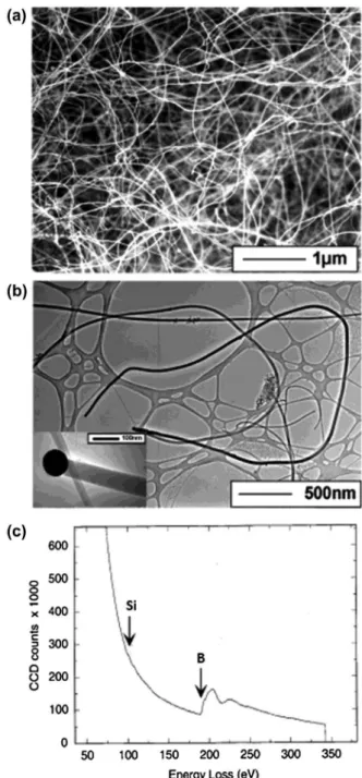
Amorphous boron nanowires with several μm length and 50–100 nm diameter were irst synthesized and clearly identiied by Wu et al. in 2001 [99]. Scanning electron microscopy (SEM) and transmission electron microscopy (TEM) images of their nanowires are shown in Figure 1(a) and (b). he nanowires were obtained as black product by growing on MgO substrate in a sealed quartz tube under BI3 vapor at 1000–1100 °C under evacuated condition at 100 mTorr. More speciically, powders of Si, I2, and B were put in one end of the tube and a MgO substrate coated by a 5-nm Au thin ilm was placed in the other end of tube, where a temperature gra-dient of 100 °C was maintained between source materials and the MgO substrate. At the hot zone, boron reacts with I2 and forms BI3 vapor. he vapor then decomposed in the low temperature zone to form boron nanowires on MgO. he obtained boron nanowires are amorphous and thus no difraction spots or rings were observed, even by selected area electron difraction (SAED). he nanowire tips were composed of Au, B, and Si, while the bodies of the nanowires were composed of B with a small amount of Si, as shown by the electron energy loss spectroscopy (EELS) results (Figure 1(c)). Based on the presence of the droplet of B/Au/Si alloy at the tip, the growth mechanism was suggested as a vapor-liquid-solid (VLS) process with Au as the liquid solvent at high temperature. he authors pointed out that the presence of Si is important to form boron nanowires because nanowires are not formed if Si was removed from the starting materials. he authors used the obtained boron nanowires as an intermediate product for the synthesis of MgB2 nanowires [99].
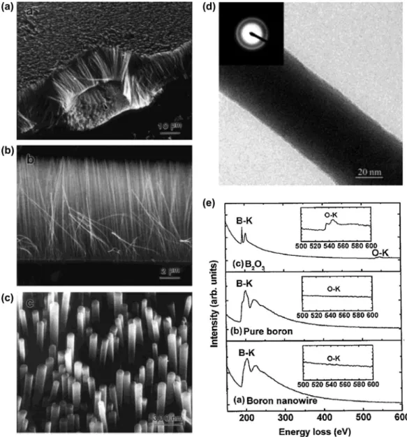
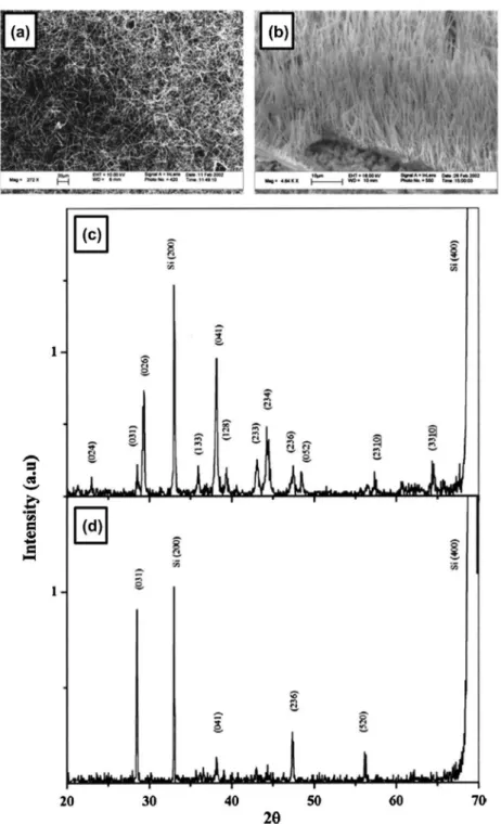
Subsequently, well-aligned amorphous boron nano-wire arrays were synthesized by Cao et al. [100] in 2001 in an argon atmosphere by a simple method of radio frequency magnetron sputtering (80 W at 800 °C and 2 Pa for 6 hours), with a target of highly pure boron and a boron oxide mixture (the authors concluded that boron nanowire arrays can also be formed without boron oxide). Boron nanowires with diameters of 20–80 nm and lengths of up to several tens of micrometers stand on the substrate Si surface to form well-aligned arrays with self-organized arrangements (Figure 2(a)–(c)). he
nanowire arrays can easily be stripped of (Figure 2(a)) with tweezers, suggesting that the boron nanowires are not strongly chemically bonded to the substrate surface. Most of the tips of wires are lat rather than hemispherical in morphology (Figure 2(c)). he TEM and SAED analysis for the boron nanowire peeled of from the arrays show a lat and smooth morphology and amorphous structure (Figure 2(d)). he amorphous phase was further conirmed by high-resolution TEM. he composition of the nanowires was revealed to be boron with a small amount of oxygen (less than 5%) based on EELS analysis (Figure 2(e)). he nanowire
Figure 1. amorphous boron nanowires synthesized by cvd
Sci. Technol. Adv. Mater. 18 (2017) 783 T. KONDO
in the radio frequency magnetron sputtering process, boron nanofeather-like arrays are grown, where each boron wire possesses Y and/or T junctions [102]. he authors concluded that this process might enable the cre-ation of nanometer-size heterojunctions of a wide variety of one-dimensional (1D) nanostructures [103]. Since no crystallization was observed up to a pressure of 103.5 GPa for these boron nanowires, the amorphous structure of boron nanowires is concluded as stable under high pressure at ambient temperature [104]. Here, it should be noted that according to a subsequent report by Wang and Duan [105], the amorphous structure of boron nanowires made by a similar radio frequency magnetron sputtering method can be converted to a rhombohedral crystalline structure (β-boron) with lattice parameters of a = 10.95 Å and c = 23.82 Å by annealing at 1050 °C
under a high vacuum for 3 hours followed by a quench. arrays in Figure 2 are then concluded to be composed
dominantly by boron atoms and no metal elements are included, which is in sharp contrast to the case of nano-wires shown in Figure 1.he authors pointed out that a high temperature at the substrate surface (above 700 °C) plays a crucial role in the nucleation and growth of boron nanowires, because the nanowire growth was not observed below 600 °C [100,101]. he growth of boron nanowire arrays is insensitive to the nature of the substrate, because the same size and shape of the boron nanowires were observed ater the growth on Si(100), Si(111), SiO2, metal plates (Ni, Fe, Co), and metal ilms (Pd, Au, Ag) on Si. he nucleation and growth of verti-cally aligned boron nanowires arrays are thus concluded to be entirely self-organized rather than catalyst-assisted processes. Interestingly, merely by increasing the Ar low rate to 60 cm3 min−1 (by a factor of approximately two)
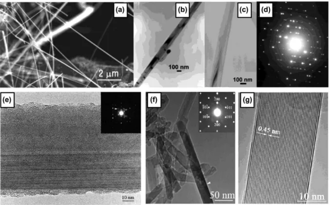
On the other hand, in the reports by Zhang et al. [113,114], single- and poly-crystalline boron nanowires were obtained as a part of the product of laser ablation. A mixture of boron rods with Ni and Co powder was placed as a target in a furnace kept at 1250 °C in a vac-uum with Ar low. A Nd:YAG laser was used for ablation of the target for 30 minutes with 532 nm wavelength, 10 Hz frequency, and 3.5 W power. Nanowires with a diameter less than 100 nm were then observed by SEM and TEM to be grown at the surface of the target. SAED analysis suggests that a portion of the nanowires are sin-gle crystal of tetragonal structure with lattice parame-ters of a = 0.875 nm and c = 0.506 nm (Figure 4(e)). At one end of the nanowire, a droplet composed of B, Ni, and Co was observed, indicating the VLS mechanism for growing boron nanowires. hey concluded that the boron nanowires with diameters ranging from several tens of nanometers to 1 μm can be synthesized by the laser ablation method on the surfaces of the targets, where the synthesis temperatures, intensities of the laser beams, and types of metal catalysts are the main synthe-sis efect factors on the growth.
Subsequently, well-aligned boron nanowires with single-crystalline structure were reported by Yang et al. in 2003 [115], using nanochannel-Al2O3 as a substrate and a CVD process. he nanochannel-Al2O3 was placed in a quartz tube furnace chamber and a mixture of Ar, H2, and diborane with a low rate of 10:10:1 was allowed into the chamber, which was maintained at 1500 Pa and 800 °C. he nanochannel-Al2O3 substrate with depos-ited materials was then dissolved in a dilute 1 M NaOH solution at 60 °C. Finally, the solution was dropped onto a copper grid for TEM measurements. Figure 4(f) is a TEM image of dispersed boron nanowires with a diameter of 25 nm. he SAED pattern illustrates that the nanowire is a single crystal tetragonal lattice struc-ture of elemental boron with the lattice constants of
a = 0.873 nm and c = 0.503 nm (inset in Figure 4(f)), which are nearly the same as the lattice parameters of the boron nanowire prepared by laser ablation as described above [113]. he distance between the parallel fringes of boron nanowire observed in high resolution TEM image (Figure 4(g)) is approximately 0.45 nm, corresponding to the spacing of the {1 1 0} planes of B with a P4n2 struc-̄ ture. he proposed formation mechanism is as follows: irst, diborane gas decomposed into boron atom clusters and H2 gas, and boron atoms reacted with the c-Al2O3 of a nanochannel-Al2O3 substrate and formed Al5BO9 layer on the surface of the channels of the nanochannel-Al2O3, which then prevented boron from reacting with Al2O3. Ater that, boron clusters conglomerated to generate boron nanowires by coninement of the channels of the nanochannel-Al2O3 substrate.
As described above, the diferent structure types of the crystalline boron nanowires, i.e. rhombohedral (β-boron) [105,116], orthorhombic [112], and tetrag-onal [113,114] structures, are formed depending on Additionally, Gao et al. [106] reported that crystalline
boron nanowires with 10 nm diameter can be directly synthesized by the same method of the radio frequency magnetron sputtering if Au catalysts are present via a VLS growth mechanism even at a lower temperature of 600 °C. Concerning the boron nanojunction, later works show that nanojunctions can also be formed by a thermal vapor transfer method [107,108] and an oxide- assisted VLS process [109].
Meng et al. [110] reported the synthesis of amor-phous boron nanowires with diameters of 30–60 nm and lengths of several tens of micrometers by a laser ablation method. A KrF excimer laser with a wavelength of 248 nm and a frequency of 10 Hz was used to con-tinuously ablate the target of pure boron in an alumina tube at 1300 °C for 5 hours under vacuum with Ar low (laser energy of 350 mJ per pulse and a pulse duration of 34 ns). Owing to the fact that the target material is only boron powder, the authors concluded that the growth of B nanowires is governed by a vapor-solid (VS) process rather than a VLS process.
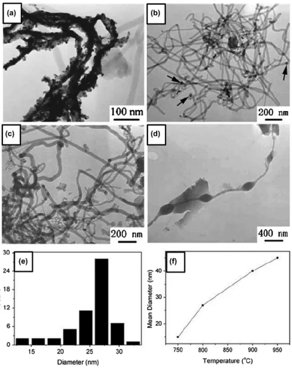
Yang et al. [111] demonstrated control over the mor-phology and diameter of amorphous boron nanowires, in CVD with VLS growth on silicon substrates, by altering the growth temperature and the thickness of the cata-lyst Au ilms on the substrate. A mixture of nitrogen, hydrogen, and diborane with a low ratio of 10:50:1 was introduced in the quartz tube with Au-coated Si substrate at 750–1000 °C and 5 × 10⁴ Pa for 5 hours. Smooth boron
nanowires were fabricated at a temperature ranging from 800 to 900 °C (Figure 3). he diameter of boron nanowires increased slightly from 10 to 50 nm as the growth tem-perature increased (Figure 3(f)). Boron nanochains with the periodically modulated diameter were also fabricated at 950 °C (Figure 3(d)). As the thickness of the Au ilms on the Si substrate increases, the diameter and length of the boron nanowires increase dramatically.
3.1.2. Synthesis of crystalline boron nanowires
In parallel with the irst reports on amorphous boron nanowires in 2001 [99,100], crystalline boron nanowires were synthesized and identiied by Otten et al. (CVD) [112] and Zhang et al. (laser ablation) in 2002 [113].
In the report by Otten et al. (CVD method), a mix-ture of 5% diborane (B2H6) in Ar gas was passed at a rate of 15 mL/min for 30 minutes over NiB powder on an alumina substrate in a tube furnace at 1100 °C [112]. he resulting brittle slag has dense entanglements of nanowires (Figure 4(a) with diameters ranging from 20 to 200 nm (mean value ~60 nm) (Figure 4(b) and 4(c)). Based on an electron difraction pattern (Figure 4(d)), the nanowires were concluded as dense, twinned, whisker crystals with an orthorhombic unit cell of a = 9.4 Å,
b = 7.1 Å, and c = 5.4 Å. he conductivity measurements of individual nanowires show semiconducting character with (1.3–5.5) × 10−5 (ohm cm)−1, which is in the range of
Sci. Technol. Adv. Mater. 18 (2017) 785 T. KONDO
indicating a signiicant efect of quenching on the improvement of crystallinity and alignment of boron nanowires.
3.1.3. Applications of boron nanowires
he excellent mechanical properties of individual crys-talline boron nanowires have been reported by a few groups [118–122]. According to the report by Liu et al. in 2013 [122], the mean fracture strength and the max-imum strain of individual crystalline boron nanowires prepared by CVD method (α-tetragonal lattice, [001] growth direction) were measured to be 10.4 GPa and 4.1%, respectively, during the tensile tests. he average Young’s modulus was calculated to be 308.2 GPa under the synthesis method and conditions. he method to
control the growth type of crystal structure of boron nanowires has not yet been well established. However, concerning the quality of the crystalline structure, Yun et al. [117] reported that single-crystalline boron nano-wires of a rhombohedral structure (a = 10.94 Å and
c = 23.83 Å) and (031) orientation aligned along the normal of the substrates can be predominantly synthe-sized by higher-temperature (⩾1100 °C) processing of a thermal vapor transport if it was followed by a quench. In the SEM images and X-ray difraction (XRD) patterns in Figure 5, a sharp contrast can be found between the cases for slow cooling of ~5 °C/min and quench ater synthesizing boron nanowires at 1100 °C for 30 minutes,
Figure 3. Size control of the diameter of amorphous boron nanowires in cvd method. TeM images of the boron nanowires
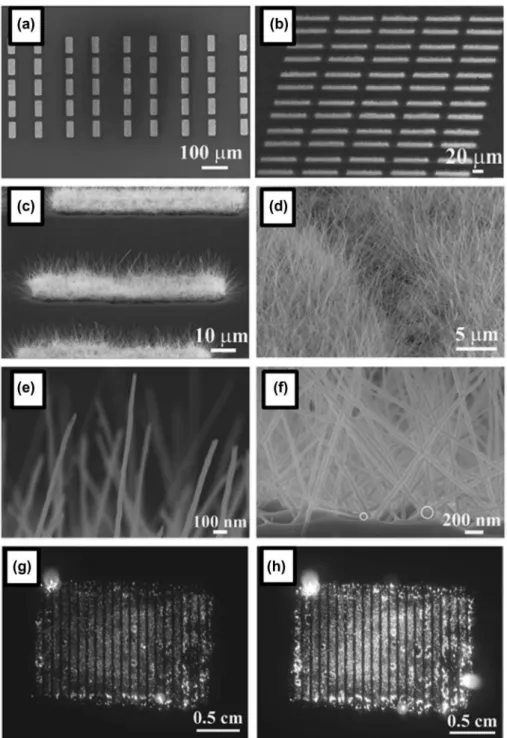
bright and uniform performance of ield emission. he side view in Figure 7(c) shows the high and uniform density of boron nanowires in each square of their pre-pared pattern. Most of the boron nanowires have an average length of approximately 6 μm with a uniform diameter of 30–40 nm (Figure 7(c) and (d)). here are no catalysts at the tips of the boron nanowires (Figure 7(e)), while Ni catalysts exist between the ends of the boron nanowires and the substrate (shown as white circles in Figure 7(f)), indicating that the boron nanowires are formed by a base-up growth mode. he authors also measured I–V curves of individual boron nanowires and estimated the electronic conductivity as 1.66 × 10⁻²
(ohm cm)−1 which is a few orders of magnitude greater
than that of bulk B of 10−4–10−7(ohm cm)−1. For the
patterned boron nanowires, a turn-on ield of 4.3 V/μm (at 10 μA/cm2 emission current density) and a threshold
ield of 10.4 V/μm (at 1 mA/cm2 emission current
den-sity) have been reported. hese values are comparable to those of many excellent cathode nanomaterials, such as ZnO nanowires, WO3 nanowires, and AlN nanowires, but are inferior to those of carbon nanotubes, graphene, and LaB6. Figures 7(g) and 7(h) show ield emission images of patterned boron nanowires at a current density of 1.4 mA/cm2 and 2.1 mA/cm2. Nearly all patterns are
simultaneously involved in the emission process and the emission brightness increases with the emission current tensile and compression tests. Bending experiments for
individual boron nanowires revealed that their maxi-mum bending strain could reach 9.9% (Figure 6) and their ultimate bending stress occurred at 36.2 GPa. hese values are much higher than those of Si and ZnO nano-wires, which are known for their high bending strength. he boron nanowires also show a very high speciic frac-ture strength of 3.9 GPa·cm3/g and speciic elastic
mod-ulus of 130.6 GPa·cm3/g, which are one to two orders
of magnitude larger compared to many reported nano-structures [122]. hese results suggest that the boron nanowires are a promising material for application as lightweight reinforcing illers.
he excellent ield emission properties of boron nanowires, such as low turn-on ield and high current endurance, have been reported [123–129]. For prac-tical applications in ield emission displays, there are two important additional issues: (i) patterned growth of boron nanowire arrays over a large area; and (ii) uniformity of physical properties of grown boron nanowires. According to the report by Liu et al. in 2014 [129], uniform crystalline boron nanowires (α-tetrag-onal lattice and the growth direction along the [001] orientation) with square (25 μm × 60 μm) patterns have been grown over a large area by CVD on a Si substrate with Ni catalysts patterned by an ultraviolet lithography technique (Figure 7(a) and (b)) and the patterns show
Figure 4. crystalline boron nanowires. Synthesized by cvd method: (a) SeM image of B nanowires, (b), (c) TeM images, and (d)
Sci. Technol. Adv. Mater. 18 (2017) 787 T. KONDO
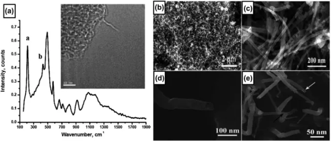
mesoporous silica template (Mg–MCM-41) as a cat-alyst and a mixture of BCl3 and H2 gases (volumetric ratio of approximately 1:6) as a source. he gas mixture was introduced at a rate of 1.5 L/min for 45 minutes in a quartz reactor (inner diameter 6 mm) with the Mg– MCM-41 catalyst at a steady state temperature of 870 °C under a continuous low of hydrogen. he reactor was then cooled to room temperature under He low. Figure
8(a) (inset) shows a TEM image of the single-wall boron nanotube obtained on the catalyst, which shows a tubu-lar structure. he Raman spectrum shown in Figure 8(a) contains distinct peak at 210 cm−1, which was attributed
to the characteristic radial breathing mode of the tubular density. It is worth noting that both the distribution of
the emission patterns and their brightness distribution are very uniform owing to the uniform growth of boron nanowires.
3.2. Boron nanotubes
Ater several theoretical studies in 1990s predicted the structure and intriguing properties of boron nano-tubes, such as metallic conductivity exceeding that of carbon nanotubes [10–16], the CVD synthesis of a pure boron single-wall nanotube was reported by Ciuparu et al. in 2004 [130]. hey used a magnesium-substituted
Figure 5. efect of quenching on crystallinity and alignment of boron nanowires. SeM images (scale bar 10 μm) and Xrd patterns
3.2 Å. he measurements of individual boron nano-tubes show that the conductivity is in the order of 102
(ohm cm)−1, showing the metallic transport property
of boron nanotubes. he conductivity is four orders of magnitude larger than that of the largest conductivity of boron nanowires described above. he individual boron nanotube also shows excellent ield emission properties, with a high stable current of approximately 80 μA and a current density of 2 × 10¹¹A/m2 which are very close to
those of carbon nanotubes.
3.3. Boron nanobelts and nanoribbons
Nanobelts and nanoribbons are materials that are mac-roscopically categorized as 1D rather than 2D (nano-sheets), since they have a rectangular cross-sectional shape and have a width-to-thickness ratio greater than one, which is also diferent from simple 1D tubes or wires. Nanoribbons have signiicantly larger width-to-thickness ratios (10–100) compared with nanobelts (~5), and thus they should have diferent chemical and physi-cal properties, depending on their size and shape as well as their bonding nature.
3.3.1. Boron nanobelts
he synthesis of single-crystalline tetragonal boron nanobelts was irst reported by Wang et al. in 2003 [132]. hey synthesized boron nanobelts by a laser abla-tion method (Nd:YAG laser with 355 nm wavelength, pulse width of 5–7 ns and 10 Hz pulse frequency) in a furnace without using a catalyst or boron vapor. he laser was introduced through a quartz glass window to the target of a hot-pressed boron pellet on a rotating holder placed at the center of the furnace. he boron nanostructures were deposited on the quartz glass sub-strate at 800 °C under Ar low at 25 Pa. A TEM image of a typical obtained boron nanobelt (Figure 9(a)) shows lat edges without the presence of nanoparti-cles and inhomogeneity, where EELS conirm that the structure. he author also attributed the spectral features
between 300 and 500 cm−1 (peak b) to tubular
struc-tures. Based on EELS results, the structure is revealed to be composed of pure boron. hus, the observed struc-ture is concluded as a pure boron single-wall nanotube. For the synthesis method, the authors pointed out the importance of the presence of Mg in the catalyst, since no boron nanotube formation was observed when they used a pure siliceous MCM-41.
he fabrication of a larger quantity of crystalline boron nanotubes was reported by Liu et al. in 2010 [131]. hey synthesized boron nanotubes with diam-eters ranging from 10 to 40 nm and an average length of several micrometers by growing on Fe3O4
nanopar-ticles with diameters less than 10 nm through high- temperature solution phase reaction at 1000–1200 °C for 4 hours, where a mixture of B2O3 and boron powders with mass ratio of 4:3 was used as the source material. Figure 8(b) shows the densely packed boron nanos-tructures on the silicon substrate, with lengths in the range of 2–4 μm. A typical high-resolution SEM image of the boron nanotubes is shown in Figure 8(c), in which some boron nanowires are mixed in the product. A side view of a typical boron nanotube is given in Figure
8(d), showing that the free end of the boron nanotube is open. A SEM image of the synthesized product with a growth time of 10 minutes is shown in Figure 8(e). he white and black arrows indicate the short boron nanotubes and boron nanowires, respectively, which coexisted at the early stage of growth. Initial growth precursors of the boron nanotubes are ascribed to the alloy nanodroplets of boron-magnetite and boron nanostructures are believed to be grown by the root-growth VLS mechanism. Based on the SAED pattern, the boron nanowires are revealed to be composed of perfect single crystals with an α-tetragonal structure and their growth direction is along [001]. he as-synthesized boron nanotubes are multi-layered nanotubes with the spacing between two adjacent layers of approximately
Figure 6. consecutive TeM images of an individual boron nanowire during diferent bending stages. reprinted with permission from
Sci. Technol. Adv. Mater. 18 (2017) 789 T. KONDO
an oxide layer is presumed to be molten or near-molten, which might enhance atomic absorption, difusion, and desorption. he synthesized crystalline boron nanobelts were revealed to be p-type semiconductors with elec-trical conductivity of the order of 10−3 (ohm cm)−1 at
room temperature, which can be enhanced by a factor of 100–500 by doping Mg [133–135].
In 2008, α-tetragonal crystalline boron nanobelts with [001] growth axis were also reported to be syn-thesized by combining the methods of e-beam evapo-ration and plasma ion bombardment [136]. Here, the boron was evaporated on an oxidized silica substrate coated with Au, which was heated to 1100 °C followed nanobelts are composed of boron. Boron nanobelts
have a width-to-thickness ratio of approximately 5 (several tens of nanometers to approximately 150 nm) and several micrometers to the order of millimeters in length. Figures 9(b) and 9(c) show the boron nanobelt with tetragonal crystalline structure (a = 0.884 nm and
c = 0.500 nm, [001] growth direction) with 55 nm width, where an amorphous structure can be seen along the surface of the nanobelt with 2–4 nm thickness. Some stacking faults were also observed along the growth direction, as shown by black arrows in Figure 9(c). he authors explained that the growth was progressed by an oxide-assisted-growth (OAG) mechanism, in which
belts, such as those with a width of 30–100 nm, thickness of 10–15 nm, and length of a few to over 15 μm were also formed.
On the other hand, in 2008, rhombohedral crystal-line boron nanobelts with a [111] growth direction and amorphous boron nanobelts were synthesized separately by controlling the condition of the method with a vapor-liquid-solid technique by Ni and Li [137]. Here, a mixture of boron, silicon, and iodine powders with the weight ratio 40:1:1 was placed into a smaller quartz boat and placed at one end of a quartz tube of diameter 19.05 mm, while a single crystal Si(100) substrate was placed at the other end of the tube ater coating with a 3- or 20-nm Au ilm (the former was used for crystalline boron nanobelt growth and the latter was used for amorphous boron nanobelt growth). Crystalline boron nanobelts were grown on Si(100) at 1100 °C with the source maintained at 1150 °C [137]. Most of the crystalline nanobelts have a width-to-thickness ratio of 2 and are covered with a layer of amorphous silicon oxide. Amorphous boron nano-belts were grown when the Si substrate temperature was 1050–1070 °C. From these results, the authors pointed out that the temperature gradient in the system is an important factor in addition to the high cooling rate to achieve crystalline boron nanobelts.
3.3.2. Boron nanoribbons
In 1990, Komatsu and Moriyoshi [9] reported that β-rhombohedral boron nanoribbons were synthesized on a Si(100) substrate, as well as whiskers and platelets by plasma-enhanced CVD with 2 kW from a gas mixture of B2H6 (0.25–1.5 vol%), H2 (5–30 vol%), and He at 700– 880 °C, where the lexible ribbon-like morphology was observed by SEM, though the precise width-to-thickness ratio was not examined.
by bombardment via a helicon plasma source. Most of the resulting nanobelts had a width of 0.1–1 μm and a thickness of 50–100 nm, while a few nanometer-sized
Figure 8. (a) raman spectrum and TeM image (inset) of boron nanotube. owing to the extreme beam sensitivity and charging of the sample, the image is blurred and out of focus. reprinted with permission from ref. [130]. copyright 2004 american chemical Society. (b) low-magniication SeM image of large-area boron nanostructures. (c) Magniied SeM image of the boron nanostructures. (d) SeM image of a boron nanotube tip. (e) high-resolution SeM image of the boron nanowires and boron nanotubes at the growth stage. Black and white arrows indicate a boron nanotube and a boron nanowire, respectively. reproduced from ref. [131] by permission of The royal Society of chemistry.
Sci. Technol. Adv. Mater. 18 (2017) 791 T. KONDO
found that all four structures of borophene nanoribbons (named P1, P2, P3, and P4) consist of the boron chains with diferent widths, separated by hexagonal hole arrays (Figure 11). More speciically, the structures of P1, P2, P3, and P4 are assigned as the same structure of so-called
χ3, β12, β, and β8 borophene sheet, respectively, predicted by the previous theoretical study [37]. To represent the nanoribbon character, the authors named them BC(2,2), BC(2,3), BC(3,4), and BC(4,4), respectively, where n and
m in BC(n, m) denote the number of atoms in the widest and narrowest regions of a single boron chain.
4. Two-dimensional (2D) boron nanomaterials
2D materials consisting of a single or a few layers of atoms exhibit superior performance compared to conventional materials or their bulk counterparts in a variety of appli-cations, because of their unique properties, including their lexibility, high speciic surface area, and quasi-2D elec-tron coninement [141–146]. In the case of boron, small clusters with 2D structures were predicted in the 1990s [13–19] and then synthesized in gas phase ater 2013 [84,94,147,148], while large-sized boron nanosheets or borophene were synthesized ater 2015 [46,47,81,149– 153]. he experimental realization of borophene stim-ulates the theoretical study and several applications of borophene, such as hydrogen storage, batteries, catalysts, electronics, superconductors, and/or mechanically strong components have been predicted together with novel structural, electronic, thermal, optical, and mechanical properties [20,49–78,80,81].
On the other hand, in 2004, single-crystalline α-tetragonal boron nanoribbons of a width of 200– 500 nm and thickness of ~20 nm were synthesized at low temperature (630–750 °C) and low pressure (200 mTorr) by pyrolysis of diborane gas in a quartz tube furnace without a catalyst by Xu et al. [138]. he nanoribbons were conirmed by EELS to be composed of boron. SEM images show that the nanoribbons are typically twisted and the edges of ribbons are sometimes not straight, but rather a zigzag shape. By applying the same method, crystalline α-tetragonal boron nanoribbons of thick-ness 16 nm were reported to be synthesized by Jash and Trenary in 2009 [139].
3.3.3. Borophene nanoribbons on Ag(110)
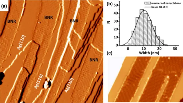
In 2017, Zhong et al. reported synthesis of single-at-om-thick borophene nanoribbons by self-assembly of boron on Ag(110) surface [140]. More speciically, boron with 99.9999% purity was evaporated using an elec-tron-beam evaporator on the Ag(110) surface, while the surface was kept at a temperature of 570 K in an ultra-high vacuum with base pressure of 2 × 10⁻¹¹ Torr. he
scanning tunneling microscopy (STM) studies reveal high quality borophene nanoribbons: all the ribbons are along the [−110] direction of Ag(110), and can run across the steps on the surface as shown in Figure 10(a). he width of ribbons is distributed in a narrow range around 10.3 ± 0.2 nm (Figure 10(b)). High resolution STM images revealed four ordered surface structures in borophene nanoribbons (Figure 10(c)). Combined with density functional theory (DFT) calculations, authors
Figure 10. Borophene nanoribbons on ag(110) surface. (a) a derivative STM image shows boronphene nanoribbons grown on
ag(110). The image size is 100 × 100 nm2. The nanoribbons run across the substrate steps without losing continuity. (b) histogram of
nanoribbon width. gaussian itting is shown as a black line. (c) high-resolution STM image of two boronphene nanoribbons. image size: 50 × 30 nm2. The bias voltages of STM images are (a) −4.5 v and (b) −1.9 v. reprinted with permission from ref. [140]. copyright
mobility of approximately 1.26 × 10⁻¹ cm2 V−1 s−1. he
photodetector device fabricated from single-crystalline ultrathin boron nanosheets further demonstrates good sensitivity, reliable stability, and fast response, obviously superior to other reported boron nanomaterials [81]. he reports by Xu et al. thus show the great potential of boron nanosheets as a material for applications in ield emitters, interconnects, integrated circuits, and opto-electronic devices.
4.2. Borophene on Ag(111)
A single-atomic two-dimensional layer of boron named borophene has been reported to be grown by the physi-cal evaporation of boron atoms on Ag(111) in ultra-high vacuum by parallel works of Mannix et al. [46] and Feng et al. [47]. hey have observed diferent phases of the borophene sheets on Ag(111). Subsequently, additional new two phases of borophene on Ag(111) are reported by Zhong et al.[153]. All of the borophene sheets on Ag(111) are reported to be metallic.
he fact that only a few structures were found on Ag(111) surface is rather surprising since freestanding borophene were predicted to be polymorphic with a tremendous number of boron structures sharing com-peting binding energy near the global minimum [37]. It may indicate that the speciic interfacial interactions between the substrate and borophene play important 4.1. Boron nanosheets
Xu et al. reported the synthesis and application of ultrathin single-crystalline boron nanosheets [81]. he nanosheets were synthesized on Si wafers by an efec-tive vapor-solid process via thermal decomposition of diborane without catalyst in a 30-mm external-diameter quartz tube at 950 °C by introducing a mixture gas (5% diborane and 95% argon) at a low rate of 5 sccm for 120 minutes at 8 Pa of the reaction pressure followed by cooling the sample to room temperature naturally (without quench). Figure 12(a) and (b) show SEM images of the nanosheets, which have a width rang-ing from tens of nanometers to 3 μm and a length of 3–20 μm. Owing to the large width, these products can be called nanosheets rather than nanoribbons. he nanosheets are almost transparent in the SEM image (Figure 12(c)), indicating the ultrathin thickness. he peaks in the Raman spectrum of the nanosheets shown in Figure 12(d) coincide with those of the α-tetragonal boron phase, which agrees with their SAED pattern anal-ysis. Based on the high-resolution TEM observations, the average thicknesses of the nanosheets are estimated as ≈8–12 nm. EELS revealed that the nanosheets consist of boron and there is no oxygen, carbon, or other impu-rities. hese nanosheets show excellent field emission performances with a low turn-on field of 3.60 V μm−1
and good stability. Moreover, the nanosheets have an intrinsic p-type semiconductor behavior with a carrier
Sci. Technol. Adv. Mater. 18 (2017) 793 T. KONDO
X-ray photoelectron spectroscopy show that these sheets are composed of boron atoms. his striped phase (boro-phene structure shown in Figure 13) corresponds to that of δ6-type borophene sheet theoretically predicted earlier [37]. Based on the scanning tunneling spectroscopy (STS) results with gapless local density of states, the authors con-cluded that the striped phase has a metallic nature. he other metastable phase, homogeneous phase, was pro-posed to arise from regular perturbations of the buckled triangular lattice, or a similar structure, occurring due to substrate interactions and phonon instabilities [46,154].
In a recent study, the striped phase observed by STM was explained by the undulated so-called β12-type boro-phene sheet (the structure of which was predicted in an earlier theoretical work [37]) on a reconstructed Ag(111) surface [152] as shown in Figure 14. Here, based on DFT calculations the authors show that the bending stifness of the β12-type borophene sheet is as small as 0.39 eV along the hollow hexagon, which is about one-fourth of the 1.5 eV for graphene, indicating the greater lexible nature of borophene compared to graphene.
In a more recent study, the self-assembly of lateral het-erostructures between homogeneous phase borophene and perylene-3,4,9,10-tetracarboxylic dianhydride (PTCDA) on Ag(111) was reported [155]. hey irst deposited boron on a Ag(111) thin ilm (~300 nm thick) on a mica substrate in UHV by electron beam evapora-tion of a pure boron rod. By maintaining the substrate at a temperature of ~480 °C, pure homogeneous-phase borophene is formed. Subsequently, PTCDA molecules roles in determining the morphology of borophene as
noted by Zhong et al. [140]. Here, the reported phases of borophene on Ag(111), namely striped, homogeneous, S1, S2, S3, and S4 phases are described.
4.2.1. Striped and homogeneous phases
In 2015, Mannix et al. [46] reported two types of monolayer crystalline boron sheets (borophene) synthe-sized by physical vapor deposition of boron on Ag(111) at 550 °C under ultrahigh vacuum. he phases are identi-ied as the striped and homogeneous phases. he striped phase consists of regions with prominent stripe features that are composed by the rectangular lattice. he homo-geneous phase is composed of chain-like atomic-scale features that are buckled vertically out-of-phase with respect to their neighbors. he relative concentration of the phases depends upon the deposition rate. Low deposition rates favored the striped phase and resulted in the growth of striped-phase nanoribbons on Ag(111). At higher deposition rates such as 0.1 monolayer/min more of the homogeneous islands are observed by STM. Increasing growth temperatures favored the striped phase, while the homogeneous phase could be observed when boron atoms were deposited at a lower tempera-ture such as 450 °C. hese results suggest that the homo-geneous phase is metastable relative to the striped phase. An STM image of the striped phase is shown in Figure
13(a). he observed STM image is well consistent with the simulated STM image (Figure 13(b)) as shown in Figure 13(c) and (d). Auger electron spectroscopy and
Figure 12. (a)–(c) SeM images for the ultrathin boron nanosheets at diferent magniications. (d) Micro-raman spectrum of the
was conirmed by the analysis with molecular dynam-ics simulations. he realization of a borophene-based heterostructure will inform emerging eforts to integrate borophene into nanoelectronic applications.
4.2.2. S1 and S2 phases
Independent of Mannix et al., in 2016 Feng et al. [47] reported two types of borophene sheets grown on Ag(111). Borophene with a diferent structure from striped phase was grown when the substrate Ag(111) were deposited by thermally evaporating PTCDA from
an alumina-coated crucible. Fine-tuning of the evapora-tion temperature and duraevapora-tion allows precise, layer-by-layer growth of self-assembled PTCDA on Ag(111). he preferential assembly of PTCDA on Ag(111) compared to borophene leads to the spontaneous formation of borophene/PTCDA lateral heterostructures. he pref-erential assembly of PTCDA was ascribed to the higher adsorption enthalpy of PTCDA on Ag(111) and lateral hydrogen bonding among PTCDA molecules, which
Figure 13. (a) Simulated empty states STM image (Vsample=1.0 v), with overlaid atomic structure and unit cell of 0.500 nm by
0.289 nm. (b) experimental STM image (Vsample = 0.1 v, It=1.0 na) of borophene was dominantly observed when it was grown at a high temperature of 700 °c, with overlaid unit cell of 0.51 nm by 0.29 nm. Top (c) and side (d) views of the low-energy monolayer structure corresponding to the δ6-type borophene sheet (unit cell indicated by the green box). from [46]. reprinted with permission from aaaS.
Figure 14. atomic geometry of periodically undulated borophene on ag(111). (a) front (top) and side (bottom) views of a β12-type borophene sheet on silver. (b) front (top) and side (bottom) views of an undulated β12-type borophene sheet on reconstructed ag(111). The topmost ag atoms are colored blue for clarity. (c), (d) Schematic continuum models for the (c) planar and (b) undulated β12-type borophene sheets on a compliant substrate. insets illustrate slices of charge redistribution between the B sheet (red) and ag (blue), where dark and light colors represent charge depletion and accumulation (0.001 e/Å3) regions, respectively [152]. copyright
Sci. Technol. Adv. Mater. 18 (2017) 795 T. KONDO
3D boron clusters is observed instead of the growth of multilayer borophene sheets, suggesting that the growth of monolayer boron sheets is assisted by the interaction with the substrate Ag(111). Later angle-resolved pho-toelectron spectroscopy measurements revealed that β12-type borophene sheets on Ag(111) (S1 phase) have a metallic nature [157] and exhibit Dirac fermions [79].
4.2.3. S3 and S4 phases
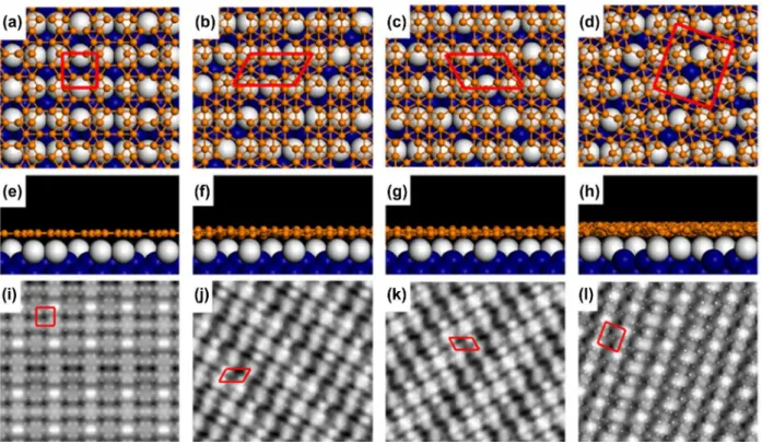
In a 2017 report by Zhong et al. [153], two additional reproducible new phases (named the S3 and S4 phases) have been found for borophene on Ag(111). Both of these phases are conirmed to be metallic based on STS measurements. hey deposited boron atoms on Ag(111) at 570 K, which is in a temperature window where the S1 phase formed as described above [47]. Figure 16(a) shows an STM image of the surface ater the boron deposition. he S1 phase (β12-type borophene sheet on Ag(111)) is indeed dominantly formed as much as 92%, temperature was 300 °C (a much lower temperature
com-pared with 550 °C for Mannix et al. [46]). Figure 15(a) is the corresponding STM image of borophene on Ag(111). his borophene was named as S1 phase and assigned as β12-type borophene sheet on Ag(111) with-out reconstruction (Figure 15(b) and (c)). he growth of β12-type borophene sheet on Ag(111) is consistent with a previous prediction of the borophene structure on Ag [156]. hey also found that the β12-type borophene sheet transformed to the diferent type of sheet named the S2 phase by annealing the sample to ~380 °C. An STM image of the S2 phase is shown in Figure 15(d). Mannix et al. noted that they have observed this S2 phase previously as the ‘homogeneous phase’ [46,154]. Feng et al. assigned the S2 phase as χ3-type borophene sheet [37] on Ag(111), the structure of which is schematically shown in Figure. 15(e) and (f). Both β12-type and χ3-type borophene sheets show a planar structure on Ag without corrugation. At higher boron coverage, the growth of
Figure 15. (a) STM image of β12-type borophene sheet on ag(111) (S1 phase) grown on 570 K. Unit cell of 0.50 nm × 0.30 nm is marked by a black rectangle. Top (b) and side (c) views of β12-type borophene sheet on ag(111). (d) STM image of χ3-type borophene
to that of S1 (6.32 eV per atom) based on the DFT cal-culations [47, 153].
he other new phase of S4 is more rarely observed compared to the S3 phase on the Ag(111) surface. As shown in Figure 16(d) of another area of the same sample, most islands in this image are S1 islands, while there is a small island exhibiting a diferent structure, as denoted by the S4 phase. Figures 16(e) and (f) are magniied STM images of the S4 phase where only the inner part of the island in Figure 16(e) exhibits a difer-ent structure, while the two edges of the island are still the S1 structure. As shown in the high resolution STM image of this phase (Figure 16(f)), it has a hexagonal crystal lattice in addition to the global moiré pattern. he rhombic unit cell, as marked in Figure 16(f) has a side length of 5.2 Å, which is very close to that of the so-called α-sheet (5.0 Å), which is the structure theoret-ically predicted [13–45]. Based on the comparison with a simulated STM image using DFT, the S4 phase was then assigned as the α-sheet on Ag(111) with buckles by 1.1 Å in the z-direction as shown in Figure 17(d)–(f). According to the atomic structure of boron sheets, the density of the hexagonal holes in S1 (1/6) is larger than S4 (1/9), which means that the β12 sheet (S1) is slightly while the other phase of 8% is one of the new phases
named S3. he S3 phase shares the identical atomic structure of the S1 phase but has a diferent rotational relationship with the substrate, and thus exhibits very diferent features in STM images as shown by the deriv-ative STM image in Figure 16(b). More speciically, the short side of the unit cell of the S3 phase is in the [1 -1 0] direction of Ag(111) (Figure 16(c)), while that of the S1 phase is in the [-1 -1 2] direction of Ag(111). As shown in Figure 16(a) and (b), no moiré patterns were then observed for S3 phase, while 1.5 nm-wide parallel stripes were observed for S1 phase which come from the commensuration between β12 structure and the lattice of the Ag(111) substrate in the [-1 -1 2] direc-tion. Interestingly, the lower population phase of S3 has a perfect lattice matching between borophene and Ag(111) compared with that for the higher population phase of S1. As shown in Figure 17(a)–(c), the triangu-lar lattice a and b for the S3 phase are 5.0 Å and 3.0 Å
for borophene, while the corresponding distances for Ag(111) are 5.02 Å and 2.9 Å. hus, no moiré patterns were observed for the S3 phase. he lower population of the S3 phase was ascribed to the slightly smaller total formation energy for S3 (6.24 eV per atom) compared
Figure 16. STM images of two metastable 2d boron sheets on ag(111). (a) STM topographic image of boron structures on ag(111).
Sci. Technol. Adv. Mater. 18 (2017) 797 T. KONDO
features orthorhombic γ-B28 cells with a unit cell of 28 atoms (a = 5.054 Å, b=5.620 Å, c=6.987 Å) and a space
group Pnnm, and it can be regarded as a boron boride (B2)δ+(B
12)δ- because of the charge transfer between these
two components [158]. he basic unit cell for b-c projec-tion is shown in Figure 18(c). he structure is built of B12 icosahedra linked into a 3D network by B2 dumbbells: the dumbbells are aligned almost parallel to the a axis, and
nearly rectangular channels along the axis are illed with boron chains. A boron thin ilm was controllably prepared over the entire surface of a Cu foil with a size of 2 × 3 cm2
(Figure 18(d)). he authors transferred it onto a 285-nm thick SiO2/Si substrate by removing the Cu foil using dilute ferric chloride (FeCl3) solution. Atomic force microscopy electron positive relative to the α-sheet (S4). From the
view of electric neutrality, the fact that the S4 resides with the S1 phase may help in stabilizing the electron surplus in S4 on the Ag(111) [47, 153].
4.3. Borophene on Cu foil
Tai et al. [150] reported atomically thin crystalline boron ilms synthesized on copper foils at 1000 °C for 1 hour by CVD using a mixture of pure boron and boron oxide powders at 1100 °C as the boron source and hydrogen gas as the carrier gas (Figure 18(a)). he structure was identiied as 2D γ-B28, which is composed of icosahedral B12 units and B2 dumbbells, as shown in Figure 18(b). It
Figure 17. Structure models of the S3 and S4 phases of boron sheets based on dfT calculations. (a) and (b) Top and side views of
of 130.6 GPa·cm3/g, which are one to two orders of
magnitude larger compared to many reported nano-structures [122]. hese results suggest that the boron nanowires are a promising material for application as lightweight reinforcing illers. he photodetector device fabricated from single-crystalline ultrathin boron nano-sheets demonstrates good sensitivity, reliable stability, and fast response [81], thus showing the great potential of the boron nanosheets as a material for applications in ield emitters, interconnects, integrated circuits, and optoelectronic devices.
Here, the concept of the building block for creating new materials is described together with the future directions of synthesis, functionalization, and mass production of boron nanomaterials rather than merely introducing theoretical predictions for the applications.
5.1. Boron nanomaterials as building blocks
As described above, boron consists of the building blocks of B12 icosahedra or icosahedral fragments, but nanoma-terials of boron (at least in the case of borophene except for the γ-B28 type) are not composed by them, owing to their low dimensionality. Here, it should be noted that a wide variety of boron nanomaterials themselves could be building blocks from the viewpoint of large-scale materi-als. Indeed, combining 2D materials through layer stack-ing in a controlled manner has already been focused on and is reported to produce several novel functionalities in the form of new 3D layered materials (van der Waals heterostructures) [159]. herefore, the synthesis of new boron nanomaterials opens several pathways for the applied use of new materials. hat is, boron nanowires, nanoribbons, nanobelts, nanotubes, and nanosheets are analysis of the transferred boron sheet on SiO2/Si shows
that the boron sheet consists of a monolayer. hus, the γ-B28 monolayer sheet can also be called borophene (γ-B28 type borophene). Interestingly, in the case of γ-B28 type borophene, the building block of B12 icosahedra is still pre-sented, contrary to the cases of β12-type, χ3-type, α-type and δ6-type borophene sheets.
5. Perspective and future directions of boron nanomaterials
A signiicant number of theoretical predictions have been reported about the advantages of boron nano-materials for applications such as hydrogen storage, batteries, catalysts, electronics, superconductors, and/ or mechanically strong components [20,49–78,80,81]. Compared to the theoretical predictions, experimental studies on the application of boron nanomaterials are limited. However, as described above, the individual boron nanotube shows excellent ield emission prop-erties, with a high stable current of approximately 80 μA and a current density of 2 × 10¹¹A/m2 which are
very close to those of carbon nanotubes [131]. he excellent ield emission properties of boron nanowires, such as low turn-on ield and high current endurance, have also been reported [123–129]. Uniform crystalline boron nanowires with square (25 μm × 60 μm) patterns have been grown over a large area by CVD on a Si sub-strate and the patterns show bright and uniform per-formance of ield emission [129]. hese results suggest that the boron nanotubes and nanowires are a promising material for application as ield emission displays. he boron nanowires also show a very high speciic fracture strength of 3.9 GPa·cm3/g and speciic elastic modulus
Figure 18. (a) Schematic representation of the two-zone furnace used to obtain atomically thin γ-B28 ilms by cvd. The temperatures of the source zone (T1) and substrate zone (T2) were set as 1100 °c and 1000 °c, respectively for the synthesis. (b) Top and side views
Sci. Technol. Adv. Mater. 18 (2017) 799 T. KONDO
characteristics of the bottom-up synthesis processes of boron nanomaterials. In the case of 2D materials, on the other hand, liquid exfoliation of 3D layered materials is widely used as a mass production method to obtain free-standing sheets, owing to its low cost and simplicity, which can be classiied as a top-down approach com-pared to syntheses involving material buildup (bot-tom-up approaches). Sheets are obtained in solution by exfoliation from 3D layered materials through sonica-tion in a surfactant solusonica-tion, ion/polymer intercalasonica-tion, or functionalization followed by exfoliation in solvent or suspension [161–164]. To date, numerous 2D materials, including graphene, hexagonal boron nitride (h-BN), transition metal dichalcogenides (e.g. WS2 and MoSe2), metal halides (e.g. MoCl2 and PbCl4), and oxides (e.g. MnO2 and LaNb2O7), have been produced by exfoliation in liquid. As the parent material in the top-down syn-thesis of borophene or borophene-related 2D sheets, we have focused on MgB2, a binary compound composed of hexagonal boron sheets alternating with Mg cations. Since MgB2 inherently contains 2D boron sheets, it is of interest to determine whether borophene could be formed by simple exfoliation and deintercalation of Mg. According to a recent report by Das et al., however, ultrasonication of water with MgB2 at room temperature produces Mg-deicient hydroxyl-functionalized boron nanosheets rather than pure boron sheets [165]. he presence of Mg and hydroxyl species in nanosheets can be explained by the instability of charged boron sheets in water derived from MgB2 by exfoliation. In our previous study, we clariied that MgB2 is exfoliated in water not by simple Mg deintercalation, but by cation-exchange reac-tions between protons and Mg careac-tions in MgB2, where the produced hydrogen boride sheets subsequently react with water to form Mg-deicient hydroxyl-functional-ized boron nanosheets as a result of hydrolysis [166]. We thus consider that the designed ion-exchange method between Mg cations and other cations is a way to pro-duce well-deined, borophene-related, and stable free-standing 2D materials through a top-down approach. In our most recent work, we report the experimental realization of 2D hydrogen boride (HB) sheets with an empirical formula of H1B1 created by the complete cation-exchange between protons and the magnesium cations in magnesium diboride (MgB2), where the ion-exchange was conducted in the acetonitrile or meth-anol without using water at room temperature [167]. he obtained hydrogen boride sheets can be considered as a new template material for the synthesis of boron nanomaterials. Moreover, the obtained hydrogen boride sheets themselves are very fascinating materials, since theoretical studies predicted that boron hydride sheets would have interesting electronic and mechanical prop-erties [168] as well as high hydrogen storage capacity [169]. Hydrogen boride sheets can also be considered as one of the building blocks of the combining materi-als, such as van der Waals hetero-structures described all building blocks and we can design and create
materi-als with new functionalities and properties by combining these boron nanomaterials with other existing nanoma-terials, molecules, atoms, and/or ions.
5.2. Transfer of borophene sheets for the application
In the case of γ-B28 type borophene grown on Cu, it was transferred to a 285-nm thick SiO2/Si substrate by removing the Cu foil using dilute ferric chloride (FeCl3) solution [150]. On the other hand, each type of borophene sheet on Ag(111) is currently just a super-structure of an adatom layer deposited on the single crystal surface from the viewpoint of surface science, because they are connecting with the substrate used for growth. It is thus uncertain whether we can obtain freestanding borophene sheets while keeping the struc-tures formed on Ag(111) because the borophene sheets grown on Ag(111) consist of the boron bonding con-iguration without the typical building blocks of B12 icosahedra.
he presence of a substrate is not a problem for elec-tronic applications, provided the substrate is compat-ible with the inal device. However, Ag(111) used for the growth of borophene is not suitable for some appli-cations, such as a ield-efect transistor. hus, we need to establish a transfer method of borophene from the substrate used for the growth, Ag(111), to the substrate desired for the application, such as an insulator. One promising transfer method has already been demon-strated in the case of single atomic layers of silicon (sili-cenes) grown on Ag(111) layers on mica, where capping the surface of silicene on Ag(111) in situ by Al2O3 enables encapsulated delamination transfer of silicene on SiO2, and native contact electrode formation can be achieved to realize back-gated silicene transistors [160]. In this case, the sheets are always connected with other elements and thus the stability originating from the interaction with the substrate can be preserved during the process. We can also apply this method to create van der Waals heterostructures or other types of new 3D materials by using borophene as one of the building blocks.
It should be noted that physical vapor deposition on Ag(111) is deinitely one of the most useful techniques for growing single-layer sheets composed by single or multiple element(s), as demonstrated by the synthesis of silicene and borophene. Further, new types of single-layer sheet materials will possibly be realized using this method.
5.3. Mass production of boron nanomaterials by top-down method
[14] Gindulytė A, Lipscomb WN, Massa L. Proposed boron nanotubes. Inorg Chem. 1998;37:6544–6545.
[15] Boustani I, Quandt A, Hernández E, et al. New boron based nanostructured materials. J Chem Phys. 1999;110:3176–3185.
[16] Boustani I, Rubio A, Alonso JA. Ab initio study of B32 clusters: competition between spherical, quasiplanar and tubular isomers. Chem Phys Lett. 1999;311:21–28. [17] Boustani I, Quandt A. Boron in ab initio calculations.
Comput Mater Sci. 1998;11:132–137.
[18] Boustani I, Quandt A. Nanotubules of bare boron clusters: Ab initio and density functional study. Europhys Lett EPL. 1997;39:527–532.
[19] Boustani I. Systematic ab initio investigation of bare boron clusters: determination of the geometry and electronic structures of Bn (n=2–14). Phys Rev B. 1997;55:16426–16438.
[20] Hosmane N. Boron science: new technologies and applications. Boca Raton, FL: CRC Press; 2011.
[21] Kunstmann J, Quandt A. Constricted boron nanotubes. Chem Phys Lett. 2005;402:21–26.
[22] Quandt A, Boustani I. Boron nanotubes. Chem Phys Chem. 2005;6:2001–2008.
[23] Kunstmann J, Quandt A. Broad boron sheets and boron nanotubes: an ab initio study of structural, electronic, and mechanical properties. Phys Rev B. 2006;74:3176. [24] Alexandrova AN, Boldyrev AI, Zhai H-J, et al.
All-boron aromatic clusters as potential new inorganic ligands and building blocks in chemistry. Coord Chem Rev. 2006;250:2811–2866.
[25] Cabria I, López MJ, Alonso JA. Density functional calculations of hydrogen adsorption on boron nanotubes and boron sheets. Nanotechnology. 2006;17:778–785.
[26] Tang H, Ismail-Beigi S. Novel precursors for boron nanotubes: the competition of two-center and three-center bonding in boron sheets. Phys Rev Lett. 2007;99:2906.
[27] Lau KC, Pandey R. Stability and electronic properties of atomistically-engineered 2D boron sheets. J Phys Chem C. 2007;111:2906–2912.
[28] Singh AK, Sadrzadeh A, Yakobson BI. Probing properties of boron α-tubes by ab initio calculations. Nano Lett. 2008;8:1314–1317.
[29] Lau KC, Pandey R. hermodynamic stability of novel boron sheet conigurations. J Phys Chem B. 2008;112:10217–10220.
[30] Yang X, Ding Y, Ni J. Ab initio prediction of stable boron sheets and boron nanotubes: structure, stability, and electronic properties. Phys Rev B. 2008;041402(R). [31] Er S, de Wijs GA, Brocks G. DFT study of planar
boron sheets: a new template for hydrogen storage. J Phys Chem C. 2009;113:18962–18967.
[32] Tang H, Ismail-Beigi S. First-principles study of boron sheets and nanotubes. Phys Rev B. 2010;115412. [33] Saxena S, Tyson TA. Insights on the atomic and
electronic structure of boron nanoribbons. Phys Rev Lett. 2010;245502.
[34] Bezugly V, Kunstmann J, Grundkötter-Stock B, et al. Highly conductive boron nanotubes: transport properties, work functions, and structural stabilities. ACS Nano. 2011;5:4997–5005.
[35] Zhang LZ, Yan QB, Du SX, et al. Boron sheet adsorbed on metal surfaces: structures and electronic properties. J Phys Chem C. 2012;116:18202–18206.
[36] Penev ES, Bhowmick S, Sadrzadeh A, et al. Polymorphism of two-dimensional boron. Nano Lett. 2012;12:2441–2445.
above. he method of synthesizing the hydrogen boride sheets can also be applied to synthesize other types of borophene-related nanosheets.
Disclosure statement
No potential conlict of interest was reported by the author.
Funding
Takahiro Kondo was supported by the PRESTO program of the Japan Science and Technology Agency (JST) [JSPS KAKENHI grant numbers JP16H00895 and JP16H03823] and MEXT Element Strategy Initiative to Form Core Research Center.
ORCID
Takahiro Kondo http://orcid.org/0000-0001-8457-9387
References
[1] Oganov AR, Solozhenko VL. Boron: a hunt for superhard polymorphs. J Superhard Mater. 2009;31:285–291.
[2] Albert B, Hillebrecht H. Boron: elementary challenge for experimenters and theoreticians. Angew Chem Int Ed. 2009;48:8640–8668.
[3] Okada JT, Sit PH-L, Watanabe Y, et al. Visualizing the mixed bonding properties of liquid boron with high-resolution X-Ray compton scattering. Phys Rev Lett. 2015;114:177401.
[4] Emin D. Icosahedral boron-rich solids. Phys Today. 1987;40:55–62.
[5] Newkrik AE. Boron, metallo-boron compounds and boranes (Ed: R. M. Adams). New York: Interscience, John Wiley and Sons, Inc.; 1964.
[6] Olempska Z, Badzian A, Pietrzak K, et al. Crystalline modiications of boron deposited on boron substrates. J Common Met. 1966;11:351–359.
[7] Komatsu S, Moriyoshi Y. Simultaneous growth of rhombohedral and amorphous boron ilms in a low pressure B2H6+H2+He plasma. J Cryst Growth. 1988;89:560–570.
[8] Komatsu S, Moriyoshi Y. Transition from thermal- to electron-impact decomposition of diborane in plasma-enhanced chemical vapor deposition of boron ilms from B2H6 +He. J Appl Phys. 1989;66:1180–1184. [9] Komatsu S, Moriyoshi Y. Growth of boron whiskers
and ribbons in a low-pressure B2H6 + He + H2 plasma. J Cryst Growth. 1990;102:899–907.
[10] Komatsu S, Moriyoshi Y. Transition from amorphous to crystal growth of boron ilms in plasma-enhanced chemical vapor deposition with B2H6 +He. J Appl Phys. 1989;66:466–469.
[11] Komatsu S, Moriyoshi Y. Growth forms of β-rhombohedral boron whiskers and platelets prepared in a low-pressure B2H6 + He plasma in terms of periodic bond chain method. J Cryst Growth. 1991;108:63–72.
[12] Komatsu S, Kasamatsu M, Yamada K, et al. Efects of plasma and/or 193 nm excimer laser irradiation on the surface in chemical vapor deposition of boron ilms from B2H 6 +He. Appl Phys Lett. 1991;59:608–610. [13] Boustani I. New quasi-planar surfaces of bare boron.