Graph Theoretic Approach for Scan Cell Reordering to
Minimize Peak Shift Power
Jaynarayan T Tudu
Indian Institute of Science
Bangalore, India
[email protected]
Erik Larsson
Linkoping University
Linkoping, Sweden
[email protected]
Virendra Singh
Indian Institute of Science
Bangalore, India
[email protected]
Hideo Fujiwara
Nara Institute of Science and
Technology
Nara, Japan
[email protected]
ABSTRACT
Scan circuit testing generally causes excessive switching ac- tivity compared to normal circuit operation. This excessive switching activity causes high peak and average power con- sumption. Higher peak power causes, supply voltage droop and excessive heat dissipation. This paper proposes a scan cell reordering methodology to minimize the peak power consumption during scan shift operation. The proposed methodology first formulate the problem as graph theoretic problem then solve it by a linear time heuristic. The exper- imental results show that the methodology is able to reduce up to 48% of peak power in compared to the solution pro- vided by industrial tool.
Categories and Subject Descriptors
B.7.3 [Reliability and Testing]: Low power testing
General Terms
Algorithm
Keywords
Peak power, Power droop, Scan chain reordering
1. INTRODUCTION
A scan chain is a set of sequential elements, which during test mode are connected to each other in a serial fashion. In scan testing, the test patterns are loaded into the scan chain by serial shifting. During the time of shifting, a num- ber of transitions occur in the scan chain. These transitions propagate and create excessive toggling in the combinational
Permission to make digital or hard copies of all or part of this work for personal or classroom use is granted without fee provided that copies are not made or distributed for profit or commercial advantage and that copies bear this notice and the full citation on the first page. To copy otherwise, to republish, to post on servers or to redistribute to lists, requires prior specific permission and/or a fee.
GLSVLSI’10,May 16–18, 2010, Providence, Rhode Island, USA. Copyright 2010 ACM 978-1-4503-0012-4/10/06 ...$10.00.
logic, which lead to high dynamic power consumption. The toggling activity that takes place during scan operation is in general much higher than the toggling during functional operation [18]. The excessive toggling during testing is the major concern for the modern circuit.
As most modern designs in the current era of deep sub- micron are functionally complex and operate at high speed, the power consumption becomes an important issue to ad- dress particularly during testing. Excessive average power can cause problems such as instant circuit damage, higher product cost, performance degradation and reduced battery life [13]; and excess peak power can result in IR drop and cross talk problems, leading to a good chip being falsely classified as defective. The IR drop and cross talk prob- lems are of increasing concern for at-speed testing. During at-speed launch and capture operation, the excessive peak power causes high rate of current in the power and ground rails and hence leads to excessive noise at power and ground. This excessive noise can change the state of logic unexpect- edly; hence, this may cause a good die to fail the test, which leads to yield loss [8]. Saxena et al. [3] discusses the IR drop and cross talk problems in detail.
Reduction of peak power during test becomes necessary for three important reasons: 1. high peak power causes yield loss due to power droop and cross talk, 2. to avoid chip be- ing damaged during testing, and 3. for an SoC with multiple module, a parallel testing can be performed to reduce the test time.
The main contribution of this paper is to provide a graph theoretic problem formulation for scan cells reordering that takes power consumption during load/unload cycle and shift
& launch cycle(also known as test cycle) into account. It also provides a heuristic to solve the formulated problem. The experimental results show that peak power can be signifi- cantly reduced.
The rest of the paper is organized as follows. Section II gives an overview of previous works. In Section III, a brief background to peak power problem and basic of scan reordering is presented. Section IV and V provides the prob- lem formulation and algorithm respectively. In section VI, time and space complexity for the proposed algorithm is an- alyzed. Section VII presents the experimental results and the paper is concluded in section VIII.
ACM Great Lake Symposium on VLSI (GLSVLSI 2010), pp. 73-78, May 2010.
2. PREVIOUS WORK
The problem of test power reduction has been an active area of research for quite sometime. The most straight for- ward approach to reduce the dynamic power is to test the circuit at reduced clock speed. However this solution is no longer a practical as modern designs are timing critical and sensitive to test application time. More over the peak power is independent of clock frequency.
Most of the previous approaches are aimed at average power reduction, however they have also achieved some re- duction in peak power as a by-product [1, 11, 9, 16, 14, 17]. The approach by Chou et al. [1] proposed the scheduling of test under power constraint, address power at module level, and not at circuit level. The work by Dabholkar et al. [11] has achieved average power reduction by test vector and scan latch reordering using some of the TSP heuristics. The work in the area of pattern compaction technique to control the average as well as peak power is done by Sankaralingam et al. [9]. The idea is to carefully merge the test patterns such that the power consumption in the resultant patterns is minimized. However, the scan reordering can still be ap- plied on power aware merged patterns to further minimize the power consumption. An technique based on scan par- tition called as adaptive scan architecture was proposed by [16]. Another work on average power reduction is done by Girard et al. [14] and Bonhomme et al. [12]. The basic idea behind these works is to reorder the scan cells. In both of these proposals, the problems are formulated as a graph theoretic problems. As the problems are NP-complete the solutions are heuristic based. Furthermore the proposal by Girard [14] also provides a power–area tradeoff. Wu et al. [17] proposed a graph theoretic formulation of scan cells re- ordering for average power reduction. In this work, the Xs are preserved during the time of scan cells reordering for further optimization using MT-fill. This work also reduces peak power consumption along with average power as by- product.
Butler et al. [5] and Li et al.[15] proposed X-filling tech- nique, specifying the don’t care bits in the test patterns, to minimize average power. Although the X-filling heuristic for average power also able to minimize peak power as by- product, the scan reordering can still be applied for further reduction.
As discussed in the previous section, peak power reduction is becoming increasingly important. A few works have been proposed in peak power reduction [10, 7, 6, 8, 2]. Sankar- alingam et al. [10] first identify the peak power violation patterns, and then perform simulation to identify the Xs in those patterns. This kind of methodology generally in- volves the simulation process which is time consuming for large circuits. More over the scan reordering can still be used along with this kind of X-fill approach. The work by Badereddine et al. [7] provids two possible approaches: scan chain stitching and X-filling technique to deal with the peak power. Badereddine et al. [6] evaluate the peak power re- duction using MT-fill. Corno et al. [2] also address the peak power problem. In this work X-bits are identified by simula- tion and specified for peak power reduction. A recent work reported by Tudu et al. [4] uses scan vector reordering to minimize peak power. However our approach of scan chain reordering can be applied along with such techniques. Hence further reduction can be achieved.
The work done by Badereddine et al. [8] is based on scan reordering to minimize peak power during test cycle. In this work, the problem is formulated as a simulated annealing problem. As the primary concern is peak power during test cycle, they have considered only test patterns and not the responses which limits their approach to reduce peak power during load/unload cycles. However, their approach could achieve nominal reduction in peak power during load/unload cycles as a by-product.
Given the above observation, in this paper we are propos- ing a methodology to explore the concept of scan cells re- ordering to minimize peak power during load/unload cycle and test cycle. The proposed methodology does not affect the stuck-at fault coverage and test time. However incur nominal routing area overhead and may affect the transi- tion fault coverage.
3. BACKGROUND
3.1 Overview of Peak Power During Scan
Operation
shif ti shif ti+1 shif t&
launch capture shif t1
Lp Cp
TCl SEn
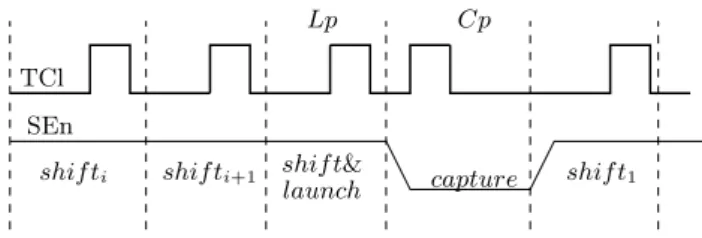
Figure 1: Timing digram for at-speed scan testing
In the above figure, TCl is test clock, SEn is scan enable, Lpis launch pulse, Cpis capture pulse and shif tiis the ith shift cycle.
The power consumed during entire scan operation at vari- ous clock cycle are, shift power during the shift cycles (which also include the launch pulse Lp) and capture power during the capture pulse Cp. The shift power at each cycle is known as instantaneous power and the maximum among all the in- stantaneous power (for all vectors) is known as peak power. The peak power during shift cycle causes excessive heat dis- sipation (when the peak power remain for several number of cycle) and the peak power during Lpcauses the IR drop problem which is especially problematic for at-speed testing [13], [3]. This paper addresses both of the problems.
3.2 Basis of Power Reduction by Scan Cell
Reordering
The scan cell reordering mechanism used for peak and av- erage power minimization basically rely on reduction of intra pattern transitions (the bit difference within a pattern). By looking at the differing bits in the patterns, each scan cell can be reconnected in a suitable order to reduce the intra pattern transitions. The reordering of scan cells brings all 1s close to each other as well as all 0s during the scan shift operation. Figure 2 demonstrates the basic principle of scan cell reordering. In this figure T is test and R is response.
Initial ordering of scan chain Reordered scan chain SF1→ SF2→ SF3→ SF4 SF1→ SF3→ SF4→ SF2
T 0 1 0 1 0 0 1 1
R 1 0 1 1 1 1 1 0
Figure 2: Basic principle of scan reordering
4. PROBLEM FORMULATION
In this section a graph theoretic problem is formulated by first constructing a graph from given scan related informa- tion and then a problem resembling to scan cells ordering is defined on that graph. The following subsections explains the complete procedure.
4.1 Construction of Graph
The important information that are needed to be reflected in the graph are, scan cells, possible scan connection and peak power information for any pair of consecutive scan cells. Below is the procedure for graph construction:-
• For every scan cell SFithere is a corresponding node Niin the graph.
• The scan path between any two possible scan cells is represented by an undirected edge between respective nodes. Note: The edges are undirected because, the pair- ing of scan cells is symmetric with respect to the number of transition. For example, in Figure 2 a revers ordering of the reordered scan chain will also results into one transition.
• The instantaneous power consumed by any test vector and response vector due to any possible pair of scan cells is represented as a pair of weight named as weight- pair of the edge between respective nodes of the scan cells. The first element of the weight-pair is the weight corresponds to test vector and the second element cor- responds to the response vector. Each element in the weight-pair are vector quantity, we name these element as testvector-weight (TVW) and responsevector-weight (RVW). The TVW and RVW are computed as follows: Computation of TVW and RVW: Each TVW and RVW keeps the instantaneous power information for all tests and responses respectively. Instantaneous power information for an individual pattern (test or response) is computed by find- ing the bit difference between the original position of scan cell pair.
Table 2 shows the TVWs and RVWs for the tests and responses shown in Table 1 respectively. The rows in Ta- ble 1 are tests Tiand their corresponding response Riand columns are scan flip flops SFi. In Table 2 the scan cell pairs
Table 1: Scan patterns and Original scan order
−→SF1−→SF2−→SF3−→SF4−→
T1 1 0 1 0
T2 0 1 0 1
T3 1 0 1 0
R1 1 0 1 1
R2 0 1 0 1
R3 1 0 0 0
Table 2: Computed TVW and RVW
scan cell pair TVW RVW
[SFi, SFj] t1 t2 t3 r1 r2 r3
[SF1, SF2] 1 1 1 1 1 1 [SF2, SF3] 1 1 1 1 1 0 [SF3, SF4] 1 1 1 0 1 0 [SF4, SF1] 1 1 1 0 1 1 [SF1, SF3] 0 0 0 0 0 1 [SF4, SF2] 0 0 0 1 0 0
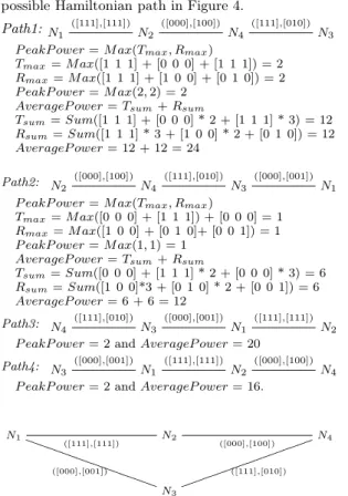
are given in column labeled with “scan cell pair” and corre- sponding TVW and RVW are given in columns t1to t3and r1to r3respectively. The columns t1to t3and r1to r3shows the peak power information for each test Tiand response Ri. The rectangular box in Table 1 shows the bit difference due to scan pair SF1 and SF2 and the corresponding transition information in Table 2 is shown inside a square box in t1mi- nor column. Figure 3 shows the complete graph constructed from the data given in Table 1 & Table 2. In the process of computation of weight-pair, we have considered tests as well as responses. Taking both tests and responses into ac- count is necessary to capture the peak power information as tests and responses both are shifted during load/unload operation.
4.2 Graph Theoretic Problem Formulation
The basic objective of problem formulation is that the for- mulation should consider the ordering of scan cells and the minimization of peak power.
The instantaneous power consumed by scan patterns dur- ing scan shift operation due to scan cell pair [SFi, SFj] is represented as the weight-pair of the edge(Ni, Nj) in the graph. For example, the instantaneous power consumed by scan pair [SF4, SF2] is represented as weight-pair ([0 0 0],[1 0 0]) shown in Table 2. As the graph is complete graph, it is always possible to find an order of scan cells by construct- ing a Hamiltonian path (which visits each node of the graph exactly once). Each Hamiltonian path in the graph has a corresponding cost, cost(Ns, Ne), of constructing the path Ns–∼–Ne, where Nsand Neare start and end nodes in the path. The computation of cost function cost(Ns, Ne) for a Hamiltonian path (let say Hp) is carried out in following manner:
• Sum up all the TVWs along the path Hp in vector addition manner and find out the maximum value in summation result.
• Similarly sum all the RVWs along path Hp and find out the maximum value in the summation result.
N1
([111],[111])
([111],[011])
([000],[001])
! !
! !
! !
! !
! !
! !
! !
! !
! !
! !
!
N2N4
([000],[100])
"
"
"
"
"
"
"
"
"
"
"
"
"
"
"
"
"
"
"
"
"
([111],[010])N3
([111],[110])
Figure 3: A complete vector-weighted graph
• The maximum of above computed maxima will be the cost(Ns, Ne) for path Ns–∼–Ne which resembles the peak power value for corresponding scan order Ss–∼– Se.
In a more formal way,
P eakP ower= cost(Ns, Ne) = M ax (Tmax, Rmax) (1)
where Tmax= M ax
l−1
X
i=1
T V W(ni, ni+1)
! and
Rmax= M ax
l−1
X
i=1
RV W(ni, ni+1)
!
, where niand ni+1are the ithand (i + 1)stvisited nodes in the path Ns–∼–Ne, and lis the length of scan chain(or total number of node). The following example illustrates the above described procedure. Example 1 Let N1
([111],[011])
N4
([000],[001])
N2 ([111],[110])
N3, be a Hamiltonian path from Figure 3. Then the Tmaxand Rmaxcan be computed as follow:
Tmax= Max(TVW(n1, n2) + TVW(n2, n3) + TVW(n3, n4))
= Max ([1 1 1] + [0 0 0] + [1 1 1]) = M ax([2 2 2]) = 2. Rmax= Max(RVW(n1, n2) + RVW(n2, n3) + RVW(n3, n4))
= Max ([0 1 1]+[0 0 1]+[1 1 0]) = Max ([1 2 2 ]) = 2. In this example n1 = N1, n2 = N4, n3= N2, and n4 = N3. Finally the cost(Ns, Ne) = M ax (Tmax, Rmax) = 2. Hence from the above illustration the graph theoretic prob- lem can formally be stated in following way:
Problem Statement: Given an undirected graph G(V, E, W), find a Hamiltonian path which has minimum cost over all other possible paths. Where V is set of vetices Vis, E is set of edges, and W is set of weight-pairs.
Note: The hardness of problem is NP-complete as this can be reduced to TSP which is a known NP-complete problem.
5. PROPOSED ALGORITHM
As the problem is NP-complete we are proposing a greedy based polynomial time (with respect to |V |) algorithm. The complete algorithm has two parts, Part-1 to find the Hamil- tonian cycle and Part-2 to find the path from Hamiltonian cycle. Following subsequent subsection gives the details of algorithm for Part-1 and Part-2.
5.1 Construction of Hamiltonian cycle
Problem Statement: Given a graph G(V, E, W) find a Hamiltonian cycle having minimum cost cost(Ns, Ne), in this case s = e.
Algorithm Part-1(with reference to Figure 3):
Step 1: Chose an initial node randomly and assign it to current-node and initialize corresponding cumulative-node- cost to ([0 0 0], [0 0 0]).
Note: cumulative-node-cost is an array of integers computed dynamically for a node visited currently.
Step 2: In this step, the decision parameter peak-power and average-power are computed. These are used in Step 3 to select the next node to visit. The peak-power and average- power are computed with respect to the set of nodes which are not yet visited and are neighbors of the current node. We call these node as candidate-node and any edge from
current node to a candidate-node is called as candidate- edge. A vector addition operation is performed between the cumulative-node-cost and weight-pair of each candidate- edge separately. We call these sum probe-path-weight. The peak-power for each of the candidate-edge is computed by finding M ax(probe-path-weight along the candidate-edge). And average-power is computed by finding Sum(probe-path- weight along the candidate-edge).
Step 3: A node Nifrom the set of candidate-node is selected as the next node if the peak-power along the edge(current- node, Ni) is minimum among all other peak-power. If there are more than one node having equal peak-power then the corresponding average-power is used as a tie breaker. In case of equal average power, the next node will be chosen randomly. Following example helps understanding the above procedure.
Example 2 Considering Figure 3, the initial node will be N1with cumulative-node-cost ([0 0 0], [0 0 0]). The neigh- boring node of N1 are N2, N3, and N4 which satisfies the property of being candidate-node because these are not yet visited. Based on the peak-power and average-power, a next node will be selected from these candidate-nodes. The cor- responding candidate-edges are edge(N1, N2), edge(N1,N3), and edge(N1,N4). The weight-pair of each of these candidate- edges are ([1 1 1], [1 1 1]), ([0 0 0], [0 0 1]), and ([1 1 1], [0 1 1]) respectively. Probe-path-weight along each of the candidate-edges will be vector addition of cumulative-node- cost of current node with the weight-pair of each of these candidate-edge which are,
([0 0 0], [0 0 0]) + ([1 1 1], [1 1 1]) = ([1 1 1], [1 1 1]), ([0 0 0], [0 0 0]) + ([0 0 0], [0 0 1]) = ([0 0 0], [0 0 1]), and ([0 0 0], [0 0 0]) + ([1 1 1], [0 1 1]) = ([1 1 1], [0 1 1]) respectively.
The peak-power and average-power along each candidate- edge can now be computed as follows,
peak-power :
along edge(N1, N2) = M ax(M ax([1 1 1]), M ax([1 1 1])) = 1 along edge(N1, N3) = M ax(M ax([0 0 0]), M ax([0 0 1])) = 1 along edge(N1, N4) = M ax(M ax([1 1 1]), M ax([0 1 1])) = 1 average-power :
along edge(N1, N2) = Sum([1 1 1]) + Sum([1 1 1]) = 6 along edge(N1, N3) = Sum([0 0 0]) + Sum([0 0 1]) = 1 along edge(N1, N4) = Sum([1 1 1]) + Sum([0 1 1]) = 5
The next task is to select a next node based on the above computed peak-power and average-power. In this example peak-power along each candidate edge is equal i.e. 1, hence average-power is used as a tie breaker. average-power along edge(N1, N3) is 1 which is less than the average-power of other candidate edge. Hence node N3will be selected as the next node to be visited.
Step 4: In this step cumulative-node-cost and current-node are updated. The cumulative-node-cost for next node to visit = cumulative-node-cost of current-node + weight-pair of edge(current-node, next-node-to-visit). For Example 2, current-node will be updated with node N3and cumulative- node-cost for N3 = ([0 0 0], [0 0 0]) + ([0 0 0], [0 0 1]) = ([0 0 0], [0 0 1]).
Step 5: Repeat the Algorithm from Step 2 until a Hamil- tonian cycle is constructed.
At the end Algorithm part-1 will produce a Hamiltonian cycle. For Figure 3 the Algorithm will give the Hamiltonian cycle shown in Figure 4 as output.
5.2 Construction of Hamiltonian path
Problem Statement: Given a Hamiltonian cycle H(V, E, W), find out a Hamiltonian path which have minimum cost cost(Ns, Ne).
Algorithm Part-2(Computation and Selection):
Computation: In this step the peak and average power consumption will be computed for every possible Hamilto- nian path. Peak power is the primary objective of power minimization where as average power is used a tie breaker which is the secondary objective. For a given H having to- tal node |V | there can be |V | number of possible Hamilto- nian path. For each path the peak and average power is computed. Computation of peak and average power for a Hamiltonian path Hpare done as follows:
Peak power is computed according to the Equation 1. Av- erage power is computed according to the weighted transi- tion metric method [9] as follows,
AverageP ower= Tsum+ Rsum (2)
where Tsum = Sum
l−1
X
i=1
TVW(ni, ni+1) ∗ i
! .
Rsum= Sum
l−1
X
i=1
RVW(ni, ni+1) ∗ (n − i)
!
, where l = |V | is the total number of node in H, and niand ni+1 are the ith and (i + 1)stnode in Hp.
Example 3 Computation of peak and average power for all possible Hamiltonian path in Figure 4.
Path1:N1 ([111],[111])
N2
([000],[100])
N4
([111],[010])
N3
P eakP ower= M ax(Tmax, Rmax)
Tmax= M ax([1 1 1] + [0 0 0] + [1 1 1]) = 2 Rmax= M ax([1 1 1] + [1 0 0] + [0 1 0]) = 2 P eakP ower= M ax(2, 2) = 2
AverageP ower= Tsum+ Rsum
Tsum= Sum([1 1 1] + [0 0 0] * 2 + [1 1 1] * 3) = 12 Rsum= Sum([1 1 1] * 3 + [1 0 0] * 2 + [0 1 0]) = 12 AverageP ower= 12 + 12 = 24
Path2: N2
([000],[100])
N4
([111],[010])
N3
([000],[001])
N1
P eakP ower= M ax(Tmax, Rmax)
Tmax= M ax([0 0 0] + [1 1 1]) + [0 0 0] = 1 Rmax= M ax([1 0 0] + [0 1 0]+ [0 0 1]) = 1 P eakP ower= M ax(1, 1) = 1
AverageP ower= Tsum+ Rsum
Tsum= Sum([0 0 0] + [1 1 1] * 2 + [0 0 0] * 3) = 6 Rsum= Sum([1 0 0]*3 + [0 1 0] * 2 + [0 0 1]) = 6 AverageP ower= 6 + 6 = 12
Path3: N4
([111],[010])
N3
([000],[001])
N1
([111],[111])
N2
P eakP ower= 2 and AverageP ower = 20 Path4: N3
([000],[001])
N1
([111],[111])
N2
([000],[100])
N4
P eakP ower= 2 and AverageP ower = 16.
N1
([000],[001])
# #
# #
# #
# #
# #
# #
# #
# #
# #
([111],[111]) N2 ([000],[100]) N4N3
([111],[010])
$ $
$ $
$ $
$ $
$ $
$ $
$ $
$ $
$ $
Figure 4: Hamiltonian cycle from Algorithm Part-1
Selection: In this step the optimal Hamiltonian path will be selected based on the following criteria,
• The path which have lesser peak power than other will be the final Hamiltonian path
• In case of multiple path having equal peak power value, the minimum average power path will the final Hamil- tonian path
• In case of failure of above criteria, the Hamiltonian path will be chosen with random choice.
For Example 3, the Path2 will be chosen as the final Hamil- tonian path as the peak power of this path is lesser than others. Hence the resultant scan chain which corresponds to Path2 will be SF2−→SF4−→SF3−→SF1.
6. TIME AND SPACE COMPLEXITY
6.1 Time Complexity
Algorithm Part-1(Hamiltonian cycle): The proposed heuristic has complexity of O(n ∗ l2) where l is the length of scan chain and n is number of test vector. The proposed heuristic takes additional 2n time to compute peak and av- erage power at Step 2 in comparison to any other heuristic of same nature whose edge weight in graph are just a scalar quantity unlike in our case.
Algorithm Part-2 (Hamiltonian path): Time complex- ity for this part of algorithm is O(n ∗ l).
6.2 Space Complexity
Proposed heuristic does not use explicit space to represent the graph as the weight of edges are computed dynamically. An array of size l is used to keep the visited information for each node. To store the cumulative-node-cost requires 2n size of array. A temporary space to keep the weight-pair needs 2n size of array. Hence the overall complexity will be O(l + n).
Hence the proposed heuristic does not suffer from any strain related to time and space.
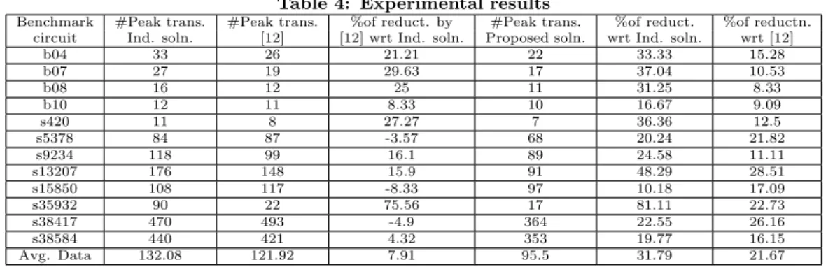
7. EXPERIMENTAL RESULTS
The experiments are carried out on ITC99 and ISCAS89 circuits. The algorithm is implemented in C++. Scan in- sertion, circuit synthesis, and test generation are performed using industrial tools. Test patterns are low power adjacent X-filled and compacted stuck-at fault pattern. Specification of benchmark circuits and experimental results are provided in Table 3 and Table 4 respectively.
Table 3: Specification of Benchmark Circuit
Benchmark #Test Scan chain #PI #PO #Gates Fault
circuit pattern length coverage
b04 49 66 11 8 628 92.85
b07 53 45 1 8 427 99.95
b08 40 21 9 4 171 100
b10 44 17 11 6 180 100
s420 53 16 18 1 218 99.32
s5378 107 179 35 49 2779 99.87
s9234 123 211 36 39 5597 99.93
s13207 115 638 62 152 7951 99.97
s15850 96 534 77 150 9772 100
s35932 13 1728 35 320 16065 100
s38417 69 1636 28 106 22179 100
s35854 111 1426 38 304 19523 100
Table 4: Experimental results
Benchmark #Peak trans. #Peak trans. %of reduct. by #Peak trans. %of reduct. %of reductn. circuit Ind. soln. [12] [12] wrt Ind. soln. Proposed soln. wrt Ind. soln. wrt [12]
b04 33 26 21.21 22 33.33 15.28
b07 27 19 29.63 17 37.04 10.53
b08 16 12 25 11 31.25 8.33
b10 12 11 8.33 10 16.67 9.09
s420 11 8 27.27 7 36.36 12.5
s5378 84 87 -3.57 68 20.24 21.82
s9234 118 99 16.1 89 24.58 11.11
s13207 176 148 15.9 91 48.29 28.51
s15850 108 117 -8.33 97 10.18 17.09
s35932 90 22 75.56 17 81.11 22.73
s38417 470 493 -4.9 364 22.55 26.16
s38584 440 421 4.32 353 19.77 16.15
Avg. Data 132.08 121.92 7.91 95.5 31.79 21.67
To show the effectiveness of the proposed work we have compared the experimental results with the scan order pro- vided by industrial tool and with the average power scan order proposed by Bonhomme et al. [12]. We have chosen [12] as the suitable reference to compare our results reason being this is the only work on scan cell reordering for min- imization of average and peak power. Another nearest can- didate would be the methodology by Badereddine et al.[8]. However, the careful observation of experimental results of [12] and [8] indicates that for most of the benchmarks the work by Bonhomme et al. [12] is performing better for shift cycle peak power.
Table 4 show that the proposed work is able to reduce the peak power up to 48.29% in comparison to the indus- trial solution and 28.51% in comparison to [12] for circuit s13207. For circuit s35932 the proposed work and the work by [12] are able to reduce the power singificantly due to the favourable combination of smaller number of pattern set and large scan chain. Also the proposed solution has achieved appreciable reduction for larger benchmark circuit. For some bench mark the %of reduction by [12] is negative because the peak power was not considered explicitly where as in this proposed work the peak power is considered as a primary parameter.
8. CONCLUSION
This paper has proposed a graph theoretic approach for scan cell reordering to minimize peak power during scan shift operation. The results show that the proposed methodology is capable of minimizing peak power in compared to indus- trial solution and [12]. The proposed work keeps stuck-at fault coverage and test application time unaffected. The scan reordering may affect the transition fault coverage in case of skewed-load testing and may incur small area over- head due to routing. In this work we have not taken these two parameters into consideration. However, the problem of routing can be solved by integrating our work with the methodology proposed by Girard et al. [14], where the pro- posed methodology can be applied within the cluster to take care of power and cluster ordering can be used to minimize routing congestion. The transition fault coverage requires further work to co-optimize it with power and routing area. The proposed scan reordering methodology is basically pattern dependent. It is the limitation of this proposed work that if some additional patterns are required on top of the existing patterns then the reordered scan chain may not be
able to reduce the peak power effectively. This issue needs further work.
9. REFERENCES
[1] R. Chou, K. Saluja, and V.D. Agrawal. Scheduling test for vlsi systems under power under power constraints. IEEE Transactions on VLSI Systems, 5(2):175 – 185, 1997. [2] F. Corno et al. On reducing the peak power consumption of
test sequences. In Proc. European Conf. on Circuit Theory and Design, pages 247 – 250, 1999.
[3] J. Saxena et al. A case study of ir-drop in structured in at-speed testing. In Proc. IEEE Int. Test Conference, pages 1098 – 1104, September 2003.
[4] J. Tudu et al. On minimization of peak power during soc test. In Proc. European Test Symposium, pages 25 – 30, 2009. [5] K.M. Butler et al. Minimizing power consumption in scan
testing: Pattern generation and dft techniques. In Proc. IEEE International Test Conference, pages 335 – 364, 2004. [6] N. Badereddine et al. Minimizing peak power consumption
during scan testing: Test pattern modification with x-filling heuristics. In Proc. of Int’l Conf. on Design and Test of Integrated System in Nano Technology, pages 359 – 364. [7] N. Badereddine et al. Controlling Peak Power During Scan
Testing: Power-Aware Dft and Test Set Perspective. Springer Berlin / Heidelberg, August 2005.
[8] N. Badereddine et al. Scan cell reordering for peak power reduction during scan test cycles. IFIP Iinternational Federation for Information Processing, 240:267 – 281, 2007. [9] R. Sankaralingam et al. Static compaction technique to control
scan vector power dissipation. In Proc. of VLSI Test Symposium, pages 35 – 40.
[10] R. Sankaralingam et al. Controlling peak power during scan testing. In Proc. IEEE VLSI Test Symposium, pages 153 – 159, 2002.
[11] V. Dabholkar et al. Techniques for minimizing power dissipation in scan and combinational circuits during test application. IEEE Trans. on Comp.-Aided Design, 17(12):1325 – 1333, December 1998.
[12] Y. Bonhomme et al. Power driven chaining of flip-flops in scan architectures. In Proc. of International Test Conference, pages 796 – 802, 2002.
[13] P. Girard. Survey of low-power testing of vlsi circuits. IEEE Design & Test of Computers, pages 82 – 92, May 2002. [14] P. Girard and Y. Bonhomme. Low power scan chain design: A
solution for an efficient tradeoff between test power and scan routing. Journal of Low Power Electronics, 1.
[15] J. LI, Q. XU, Yu HU, and X. LI. On reducing both shift and capture power for scan-based testing. In Proc. Design Automation Conference, pages 653 – 658, 2008.
[16] L. Whetsel. Adapting scan architecture for low power scan operation. In Proceedings International Test Conference, pages 863–873, 2000.
[17] Y. Wu and M. Chao. Scan-chain reordering for minimizing scan shift power based on non-specified test cubes. In Proc. IEEE VLSI Test Symposium, pages 147 – 174, April-May 2008. [18] Y Zorian. A distributed bist control scheme for complex vlsi
devices. In Proceedings of the 11th IEEE VLSI Test Symposium, pages 4 – 9, 1993.