Thermal-Aware Test Scheduling for NOC-Based 3D Integrated
Circuits
Dong Xiang and Gang Liu
School of Software, Tsinghua University, Beijing 100084, China [email protected]
Krishnendu Chakrabarty
Dept. of ECE Duke University Durham, NC 27708, USA
Hideo Fujiwara
Faculty of Informatics Osaka Gakuin University
Osaka 564-8511 Japan [email protected]
Abstract
A 3D stacked network-on-chip (NOC) promises the integration of a large number of cores in a many-core system-on-chip (SOC). The NOC can be used to test the embedded cores in such SOCs, whereby the added cost of dedicated test-access hardware can be avoided. However, a potential problem associated with a 3D NOC-based test access is the emergence of hotspots due to stacking and the high toggle rates associated with structural test patterns used for manufacturing test. High temperatures and hotspots can lead to the failure of good parts, resulting in yield loss. We de- scribe a thermal-driven test scheduling method to avoid hotspots, whereby the full NOC bandwidth is used to deliver test packets. Test delivery is carried out using a new unicast-based multicast scheme. Experimental re- sults highlight the effectiveness of the proposed method in reducing test time under thermal constraints.
I. Introduction
Networks-on-chip (NOC) have emerged as a promis- ing communication paradigm for core-based system chips. A 3-dimensional network-on-chip, the combina- tion of NOC and die-stacking 3-D IC technology [4, 13], is motivated by the need to achieve low latency, low- power consumption, and high network bandwidth.
An inefficient solution to the above problem cannot use the full NOC bandwidth for testing and instead de- liver tests to cores sequentially. This solution is likely to increase test time considerably and increase test cost. In this paper, we present a thermal-driven test scheduling method to reduce the chip temperature during testing, and especially the peak temperature of the hotspots.
A number of design-for-testability (DfT) techniques have been proposed in the literature for NOC test- ing [4, 12]. Techniques have also been proposed to in- crease interconnect reuse for NOC testing [3, 4]. Reuse of the communication platform [3] is a cost-effective tech- nique for targeting the cores in a multicore chip with an NOC. Test solutions have targeted routers, cores [3] and
This work is supported in part by the National Science Foundation of China under grants 60910003 and 61170063, and the research grant from the Ministry of Education under grant 20111081042.
interconnects [5]. Different test packets must be deliv- ered to separate cores in the methods described in [4], which can make test cost prohibitive.
A number thermal-aware test scheduling techniques have been proposed [1, 2, 7, 10, 13] for test scheduling of SoCs. The method in [13] introduced a technique to rapid generation of safer test schedules without time- consuming thermal simulations. Liu et al. [10] proposed thermal-aware test scheduling scheme for NOCs by using variable clock frequencies, which suffers from implemen- tation challenges and may not be cost-effective.
More recently, Xiang, et al. in [15] proposed a unicast-based multicast scheme for test delivery to logic cores using the NOC as the interconnect fabric. How- ever, a drawback of [15] is that it was limited to power- aware scheduling and thermal constraints were not con- sidered. Moreover, the scenario of a 3D stacked chip (with a 3D NOC) was not considered and output re- sponses were not compacted before being sent back to the tester. Another limitation of [15] is that it does not describe any DFT architecture for global test control.
A unicast scheme delivers a packet from a single core, called the source, to a single destination. A multicast scheme delivers a packet from a single core, i.e., the source, to multiple cores in the NOC. A unicast-based multicast scheme completes multicast by using multiple unicast steps. Therefore, it is not necessary to modify the unicast router architecture [11] to support unicast- based multicast.
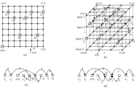
Consider an 8X8 mesh as shown in Fig. 1(a), which is placed as a 4x4x4 mesh and a 4x4 sub-mesh is contained in each layer as shown in Fig. 1(b). Two unicast pack- ets can be delivered from v to u, and from z to w with disjoint links by using X-Y-Z routing in a 3-D stacked NOCs. Let us consider a 4x4x4 mesh. The address se- quence (0,1,0), (0,1,2), (1,3,2), (1,3,3), (2,0,3), (2,2,3), (2,3,3), (3,0,2), (3,2,2) is a dimension-ordered chain.
In this paper, we address the problem of thermal- aware test scheduling and DFT innovations for NOC- based 3D stacked ICs. The main contributions of the pa- per include: (1) a thermal-driven test scheduling scheme is proposed based on a unicast-based multicast; (2) A new low-power and low-cost scan testing scheme for a core is proposed for logic cores.
The rest of the paper is organized as follows. The new thermal-driven test scheduling procedure is presented in Proceedings of 2013 IFIP/IEEE 21st International Conference on Very Large Scale Integration (VLSI-SoC)
(0,0)
(0,7) (7,7)
(7,0) 57
10 19
43 21
14
46 16
(0,0,0)
(a) (b)
62 ATE
ATE v
1 2
5
3 8
6 z
x
y
(0,3,3) (3,3,3)
(3,0,0) 2 3
1
3
4 4
3 1
1 3
3
1 v’4
v’
v’ v’7
v’
v’ v’
v’
v’1 v’2 ATE v’3 v’5
1 4
2 v’6 v’7 v’8
4 3 3
v’4
4 4
(c)
v’1 v’2 ATE v’3 v’5 v’6 v’7 v’8 1
1
1
1
2 2
3 v’4 1
4
(d) layer 4
layer 3 layer 2
(0,0,3) layer 1
(3,3,0)
Figure 1: A 3-D stacked 8x8 mesh-based NOC: (a) 2-D stacked NOC, (b) 3-D stacked NOC, (c) the unicast-based multicast scheme to deliver test packets, and (d) test response collection graph.
Section II. A low-power scan testing scheme and con- trol technique for 3-D stacked NOC core testing are de- scribed in Section III. An X-tolerant compactor is pro- posed to compact test responses on-chip in Section III. In this way, the amount of response data can be reduced significantly. Experimental results are presented in Sec- tion IV. Finally, the paper is concluded in Section V.
II. Thermal-Aware Test Scheduling The thermal-driven test scheduling solution is ob- tained by partitioning test delivery into multiple phases. Temperature is updated after a test phase. Test packets are not delivered to any hotspot in the next test phase. The most important reason why we emphasize low-power testing is that low power consumption introduces low peak temperature. Therefore, a new scan testing tech- nique is proposed in Section IV.
Unlike previously published unicast-based schemes, e.g., [11], the new unicast-based multicast source is in- volved in test delivery only in the first unicast step like that in [15]. Test packets for a class of core are delivered first, and test packets for remaining test vectors of the second core class are delivered in a subsequent step. This process continues until test packets for all cores have been delivered. The multicast tree is kept in the header flits, as in the method in [11], which is implemented by simply forwarding the dimension-ordered chain to the root of the multicast tree. A subset of ordered destina- tions is forwarded to the corresponding successors. This process continues until all destinations have received test packets.
The thermal-driven test scheduling procedure avoids delivering a test packet to hotspots. Thus we partition
the test process into multiple phases and use HotSpot [6] to update thermal information of the NOC after each phase has been completed.
The procedure for thermal-driven test scheduling is shown in Fig. 2. The current packet p is selected when the delivery of p has no conflict with all other test packets being delivered in the NOC during the same unicast step, and the power constraints can be satisfied. We say that p has no conflict with other packets in the NOC if p does not need to use any link that is used by the packets in the NOC in the same unicast step.
For an NOC with multiple classes of cores, our method just activates one class of cores at a time. The proposed low-power scan testing scheme also just acti- vates a part of scan flip-flops when the NOC contains just a single class of cores. Therefore, Our method does not consider whether the power constraint can be sat- isfied unlike [3]. A test packet is delivered to a class of cores, and no core in any of the class is a hotspot.
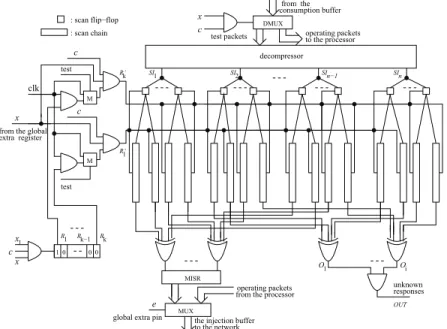
Implementation of the technique to collect test re- sponses in [15] can be complex. As shown in Fig. 3, the test responses at a core is compacted by a MISR in the new method, where test responses of all test vectors are compacted into a single vector kept in the MISR. Test responses of the same class of cores are delivered back to the ATE like the scheme presented in [15], which uses the reverse operation of the unicast-based multicast scheme. The successors of a node in the multicast tree to deliver the test packet become its predecessors in the test re- sponse, where the unique predecessor of each node in the multicast tree become its unique successor.
As shown in Fig. 1(d), all test response packets from the cores of the same class are delivered along the reverse paths in the multicast tree. All successors of a core in the
thermal-aware-test-scheduling()
1. Partition the test packet set P into subsets P1, P2, . . ., Pk, i ← 1;
2. While the test packet set i ≤ k, and Piis not empty, do 3), 4), 5), 6) and 7)
3. Update the thermal information of the NOC by running HotSpot [6]. Select a packet p ∈ Pi.
(a) If one or more of the destinations for p is a hotspot, delete it from the destination set, and keep the test packet and the hotspot.
(b) Deliver the test packet from the ATE to the re- maining cores.
4. Deliver the packet to the hotspot cores when they have been not hotspots in one of the later phases.
5. If delivering the packet p does not cause any conflict, and addition of test power generated by p with test power produced by the test packets delivered in the NOC is no more than the given threshold, do
Put the test packet p into the test packet queue, delete pfrom the packet set P .
6. Else do,
(a) Compute the necessary period when the test packet p can be delivered.
(b) Randomly select k packets from the remaining packets, compute their delivery time in the cur- rent situation separately. Select the test packet p′, which has the earliest delivery time among the k test packets.
(c) If the time is earlier than the time that the current packet p can be delivered, put the test packet p′ into the queue instead of p, and put the test packet pinto the unscheduled test packet set.
7. i ← i + 1.
Figure 2: The thermal-aware test scheduling procedure.
multicast tree for test data delivery are its predecessors in the test response collection graph. The test response packets to its unique predecessor in the process of test packet delivery given in Fig. 1(c).
The amount of test responses required delivering in the network can be significantly reduced based on the MISR-based test response compaction scheme compared to the technique to deliver the test response packet sep- arately for each test packet [3].
III. Low-Power Core Testing
In this section, we consider low-power testing in or- der to reduce the impact of hotspots and facilitate test scheduling for a 3D stack. We propose a new low-power scan testing scheme with compressed test stimulus data. It uses a combination of a coding-based scheme and the scan forest architecture to further compress the stimulus test data, therefore, the test data that must be delivered
in the network can be further reduced. However, it is necessary to insert a decompressor into each core, where the area overhead for the decompressor is very small.
A. Scan Architecture to Tolerate Unknowns
The test responses for logic cores can include a signif- icant percentage of unknown (X) bits. The MISR-based compactor must avoid unknowns [14]. The unknown re- sponses may originate from uninitialized memory ele- ments, floating bus drivers, false and multi-cycle paths and other sources that are found in real designs. Unlike the method in [3], the new method adopts a MISR to each core and the MISR is designed to be X-tolerant. We assume that the locations of the PPOs, which pro- duce unknowns, are known.
Our method clusters the potential unknown sources into the same scan chains. It also groups scan flip-flops that produce unknowns into the same chains to tolerate unknowns. We use the coordination measure to estimate the possibility for any pair of scan flip-flops to produce unknowns. Unlike the test response compactor, we do not consider simultaneous observation of any pair of scan flip-flops for a test vector because the MISR-based test response compactor is used.
The scan-out pins are connected to the XOR trees for test response compaction. The output of the test response compactor is connected to the inputs of the MISR. Therefore, it is not necessary to deliver a test re- sponse packet for each test packet. Our method delivers the compacted final test responses in the MISRs back to the ATE. The time to deliver test response packets can be reduced significantly.
A gating technique is proposed to reduce test power as shown in Fig. 3, which can still compress test data. The proposed method requires an extra register for the gating technique used for low-power testing. A combina- tion of the scan trees [16] and an existent coding-based test compression scheme can be used to compress test stimulus data. As shown in Fig. 3, the scan chains are partitioned into k subsets, where k is the size of the ex- tra register. Each subset of scan chains are driven by a single clock signal. It is not necessary for scan chains driven by the same scan-in pin fall into the same subset. Our method inserts an extra multiplexer into the out- put of the AND gate for each clock signal. The selection signals of the multiplexers are the same as that for the scan chains. That is, the clock signal clk ANDed with one of the signals R1, R2, . . ., Rk drives each subset of scan chains when test = 1, and regular clock signal feeds to all scan chains when test = 0.
Only a subset of scan flip-flops are activated in any shift cycle. The low-power scan testing scheme provides test application cost at the level of multiple scan chains. The size of the extra register is not very large. Compared to the method by [10], the test data required delivering to a core is much less because of the new test compres- sion scheme, and the amount of test response data is much less. As shown in Fig. 3, O1, O2, . . ., Oiare out-
R R
R1 k−1 k
0 1 0 0
M test clk
R’1 M
test c c : scan chain : scan flip−flop
R’k
to the processor DMUX
consumption buffer from the
operating packets
MISR
MUX
c x
test packets
from the processor operating packets
the injection buffer to the network
OUT responses unknown
O i O 1
global extra pin e x
extra register
x1 c
x from the global
SI 1 SI 2 SI n−1 SI n
decompressor
Figure 3: The low-power scan testing architecture at each core.
puts of the test response compactor that may produce unknowns, which are not connected to the MISR.
The scheme to apply each test vector can be stated as follows: (1) Activate a subset of scan chains, disable all other scan chains; apply the test vector to the activated scan chains. (2) Continue the above process until the test vector has been applied to all scan chains. (3) All scan chains capture test responses.
B. Techniques to Control the Scan Testing Scheme The number of extra pins must be well-controlled. Each core requires a number of scan-in and scan-out pins, which can make the total number of extra pins very large when the number of cores in the NOC is large enough. The number of test selection pins of the scan flip-flops for all cores can also be very large if each core uses a separate test selection pin. It should be noted that only cores of the same class can be tested concurrently. Test data are compressed by the combination of scan forest and a coding-based test compression scheme. The test responses are compacted by the X-tolerant MISR- based compactor as stated earlier in Subsection A. The test compression scheme can further compress the test data compared to the method that used only scan forest. As for scan testing inside each core, our method par- titions all scan trees into M subsets, where only one subset of scan trees is activated in a single cycle during the shift cycles. Power consumption inside the core can be reduced to about 1/M in most cases compared to the original test power. However, test application time can increase about M times. Test application cost is not comparable to the test delivery cost in the network- on-a-chip, therefore, the low-power scan testing scheme does not increase test cost inside a core because the pro-
posed test compression scheme can greatly reduce test application cost.
In our method, all cores share the same test selection pin as shown in Fig. 3. Therefore, the number of ex- tra pins to control scan testing in a NOC is just one. The extra pin x1 that drives the extra register can also be shared by all cores, according to which another ex- tra pin is necessary. An extra pin x is connected to all AND gates, which drive the scan chains directly. Each core needs a separate extra pin x. A global extra scan chain can be used, where each extra scan flip-flop of the global scan chain is connected to the extra pins. It is not necessary to load the control vector for each test packet, while each test phase (thermal information is updated each phase). The scan chains in the core are disabled if the extra pin x is loaded value 0. All scan chains are controlled by the signals from the extra register if value 1 is loaded to the extra pin x. That is to say, just a global scan-in pin and a scan-out pin are necessary.
We still need k extra pin c as shown in Fig. 3, where each extra pin drives each class of cores and k is the number of different classes of cores (k is set to no more than 4 in this paper). In any case, just one of the extra pins is set to value 1, and all other pins are set to 0. All scan-in pins in a core are connected to the consumption channel at each core, where the consumption channel is the interface from the network to an internal core. The scan-in pins can be controlled by a demultiplexer as shown in Fig. 3, and the input of the demultiplexer is the consumption channel. One of the outputs of the de- multiplexer is scan-in pins, and the other is the channel connected to the processor to deliver operating packets. The selection pin of the demultiplexer is the output of the AND gate whose inputs are x and c signal. There- fore, the scan-in pins at each core do not produce any
Table 1: Performance Comparison with [3] and [15] in a 8x8 NOC
core class [3] [15] proposed
delivery area CPU (second) 4 640352000 2239880 450456 4.24 63.5 3 655796000 564173 293446 4.26 41.4 2 928693970 730538 348945 3.80 49.2 1 729071870 236633 221119 2.40 31.2
Table 2: Test Data Volume Comparison
class Cota [3] Xiang [15] proposed
test TR test TR test TR
4 1225343280 1290271254 5234643 6957161 1397806 140 3 1255155336 1321958960 1668324 4596307 844313 90 2 1777508736 1872520960 1663329 4554613 841656 60 1 1395138816 1545158528 840500 1670703 600357 30
extra pin at the inputs of the NOC.
All scan-out pins of the X-tolerant MISR are con- nected to the injection buffer at each core. The outputs O1, . . ., Oi are connected to an extra AND gate, whose output is not delivered back to the ATE. Therefore, all cores can share the same extra pin for the unknown re- sponses. The injection buffer is the interface for each node from the core to the network. The test response packet from each core is inserted into the network from the injection buffer, which is delivered back to the ATE. Connection between the output of the MISR is controlled by a single global extra pin via a multiplexer, whose an- other input is the injection channel.
IV. Experimental Results
We have implemented the proposed method, and as a baseline, the methods in [3] and [15]. The single stuck-at fault model is considered in this paper. At most three test or test response packets can be kept at the injection buffer from each processor to the NOC.
The final data kept in an MISR are injected to the NOC from a core via the injection buffer and delivered to its successor in the test response collection graph as shown in Fig. 1(c). Test response packets delivered to the same core are compacted into a single packet, which is injected to the NOC and delivered to its unique suc- cessor in the test response collection graph.
0.0 20.0 40.0 60.0 80.0 100.0 120.0
20% 40% 60% 80% 100%
peak temperature
percentage of applied test
Proposed [23] [3]
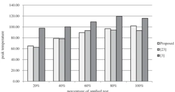
Figure 4: Peak temperature for NOCs with four classes of cores.
0.00 20.00 40.00 60.00 80.00 100.00 120.00
20% 40% 60% 80% 100%
peak temperature
percentage of applied test
Proposed [23] [3]
Figure 5: Performance temperature for NOCs with three classes of cores.
We have implemented the proposed method by using the three largest IWLS2005 circuits ethernet, des perf, vga lcd, and the largest ITC99 circuit b19. It can be extended to NoCs with more different classes of cores. All selected benchmark circuits are randomly assigned to the cores in a 8x8 mesh. Table 1 presents the test de- livery time (cycles) of the proposed method, the method in [15] and the method proposed by Cota [3] in the first three columns. Area overhead (percentage) of the new is presented in the column area. The CPU time (sec- ond) to estimate temperature of the proposed method is presented in column CPU based on the system thermal analysis tool HotSpot [6]. Circuits b19, des, and vga are randomly inserted into the cores when the NOC contains three separate classes of cores. Circuits b19 and vga are randomly inserted into the NOC when it contains two different classes of cores. In a NOC that contains a sin- gle class of cores, circuit b19 is inserted into all cores. The method in [3] needs much more time to deliver test packets and test response packets than the new method and the one in [15] in all cases.
Table 2 presents the test data volume of three meth- ods. Test response data (TR) is much less than both of the previous methods. The sizes of the MISRs for differ- ent cores b19, des, ethernet, and vga are set to 30, 30, 50, and 30 in the proposed method. For a NOC with a single class of cores (b19), the amount of test response data is just 30 bits when we consider testing instead of diagnosis!
As for the method in [3], test packets must be sep- arately delivered from the ATE to all cores. The test response packets must also be sent from each core to the ATE separately. The method in [15] used determinis- tic routing to deliver test packets for each unicast step, which delivers a test response packet back to the ATE immediately after the test vector has been applied.
We consider each physical channel have two virtual channels in the 3-D stacked NOC. The SL and RL are included, which are set to ten clock cycles in all simula- tion results. The consumption buffer for each core can keep up to three test packets, while the injection buffer provides enough buffer to keep three packets. Two adja- cent routers transfer a single flit data in a cycle, where a flit contains 32 bit data.
Figs. 4-7 present peak temperature introduced by the
0.00 20.00 40.00 60.00 80.00 100.00 120.00 140.00
20% 40% 60% 80% 100%
peak temperature
percentage of applied test
Proposed [23] [3]
Figure 6: Peak temperature for NOCs with two classes of cores.
0.00 20.00 40.00 60.00 80.00 100.00 120.00
20% 40% 60% 80% 100%
peak temperature
percentage of applied test
Proposed [23] [3]
Figure 7: Peak temperature for NOCs with a single class of cores.
test process in a 3-D stacked NOC when the NoC con- tains four, three, two and one different classes of cores. It is found that the proposed method obtains more than 20 degree reduction compared to the method in [3], and apparent peak temperature reduction compared to the method in [15].
V. Conclusions
3D stacking for networks-on-chip (NOCs) offers un- precedented opportunities for high-performance and low-power system operation. However, unbalanced heat dissipation in 3D stacked NOCs introduces hotspots that affect reliability. This problem is likely to be espe- cially severe during test application due to higher cir- cuit activity in test mode, and the transfer of a large amount of tests to logic cores in 3D stack through a 3D NOC. We have described a thermal-aware test schedul- ing method to reduce peak temperature and reduce the impact of hotspots during test application. The pro- posed technique avoids the delivery of test packets to hotspots in the NOC in each unicast step. We have shown that, for representative benchmark designs, the proposed method can significantly reduce the peak tem- perature, test time, and test data volume compared to previous method [3, 15].
References
[1] N. Aghaee, Z. Peng, and P. Eles, “Adaptive temperature-aware SoC test scheduling considering pro-
cess variation,” in Proc. 14th Euromicro Conf. on Digital System Design, pp. 197-204, 2011.
[2] D. R. Bild, et al., “Temperature-aware test scheduling for multiprocessor SOCs,” in Proc. of ICCAD, 2008. [3] E. Cota and C. Liu, “Constraint-driven test scheduling
for NOC-based Systems,” IEEE Trans. on CAD, vol. 25, no. 11, pp. 2465-2478, 2006.
[4] J. Dalmasso, E. Cota, M. L. Flottes, and B. Rouzeyre,
“Improving the test of NOC-based SoCs with help of compression schemes,” in Proc. of Annual Symp. on VLSI, pp. 139-144, 2008.
[5] C. Grecu, A. Ivanov, R. Saleh, and P. P. Pande, “Testing network-on-chip communication fabrics,” IEEE Trans. on CAD, vol. 26, no. 12, pp. 2201-2214, 2007.
[6] W. Huang, M. R. Stan, K. Skadron, K. Sankara- narayanan, and S. Ghosh, “HotSpot: A compact ther- mal modeling method for CMOS VLSI Systems,” IEEE Trans. on VLSI Systems, vol. 14, no. 5, pp. 501-513, May 2006.
[7] L. Jiang, Q. Xu, K. Chakrabarty, and T. M. Mak,
“Integrated test architecture optimization and thermal- aware test scheduling for 3D SOCs under pre-bond test- pin-count constraint,” IEEE Trans. on VLSI Systems, vol. 20, no. 9, pp. 1621-1633, Sept. 2012.
[8] A. B. Kahng, B. Li, L. S. Peh, and K. Samadi, “Orion 2.0: A fast and accurate NOC power and area model for early-stage design space exploration,” in Proc. of DATE, 2009.
[9] M. R. Kakoee, V. Bertacco, and L. Benini, “A dis- tributed and topology-agnostic approach for on-line NOC testing,” in Proc. of Int. Symp. on Networks-on- Chip, pp. 113-120, May 2011.
[10] C. Liu and V. Iyengar, “Test scheduling with thermal optimization for network-on-chip systems using variable rate on-chip clocking,” in Proc. of DATE, 2006. [11] P. K. McKinley, H. Xu, A. H. Hossein, and L. M. Ni,
“Unicast-based multicast communication in wormhole- routed networks,” IEEE Trans. Parallel and Distributed Systems, vol. 5, no. 12, pp. 1252-1265, 1994.
[12] K. Peterson and K. Oberg, “Toward a scalable test methodology for 2D-mesh network-on-chips,” in Proc. of DATE, 2007.
[13] P. Rosinger, B. Al-Hashimi, and K. Chakrabarty,
“Thermal-safe test scheduling for core-based system-on- chip integrated circuits,” IEEE Trans. on CAD, vol. 25, no. 11, pp. 2502-2512, Nov. 2006.
[14] N. A. Touba, “X-cancelling MISR–an X-tolerant methodology for compacting output responses with un- knowns using a MISR,” in Proc. of Int. Test Conf., pa- per 6.2, 2007.
[15] D. Xiang and Y. Zhang, “Cost-effective power-aware core testing in NOCs based on a new unicast-based multicast scheme,” IEEE Trans. CAD, vol. 30, no. 1, pp. 135-147, Jan. 2011.
[16] D. Xiang, K. Li, J. Sun, and H. Fujiwara, “Reconfigured scan forest for test application cost, test data volume and test power reduction,” IEEE Trans. on Computers, vol. 56, no. 4, pp. pp. 557-562, April 2007.
![Table 1: Performance Comparison with [3] and [15] in a 8x8 NOC](https://thumb-ap.123doks.com/thumbv2/123deta/5753573.27163/5.918.479.769.110.260/table-performance-comparison-x-noc.webp)