A Binding Method to Generate Easily Testable
Functional Time Expansion Models
Mamoru Sato
Graduate School of Industrial Technology Nihon University
Chiba, JAPAN [email protected]
Tetsuya Masuda
Graduate School of Industrial Technology Nihon University
Chiba, JAPAN [email protected]
Jun Nishimaki
Graduate School of Industrial Technology Nihon University
Chiba, JAPAN [email protected]
Toshinori Hosokawa College of Industrial Technology
Nihon University Chiba, JAPAN
Hideo Fujiwara Faculty of Informatics Osaka Gakuin University
Osaka, JAPAN [email protected]
Abstract— A test generation method for datapaths using easily testable functional time expansion models was proposed. In the test generation method, several easily testable time expansion models are generated for datapaths and test sequences are generated using the models. Moreover, the controller is augmented so that the behavior of easily testable functional time expansion models can be controllable. However, when circuit structures of datapaths are not easily testable, it is hard to generate easily testable functional time expansion models with small numbers of time frames even if a controller is augmented. In this paper, sequential depths of operational units are proposed as testability measures for circuit structures of datapaths, and a binding method for testability to reduce the sequential depths is proposed. Experimental results show that the proposed binding method is effective for sequential depths of operational units, fault coverage, and test generation time compared to a conventional binding method without testability consideration.
Keywords—high-level synthesis; test generation; easily testable functional time expansion models; sequential depths of operational units; binding
I. INTRODUCTION
Recent advances in semiconductor technologies have resulted in exponential increases of density and complexity of very-large-scale integrated (VLSI) circuits [1]. As a result, design costs of VLSI circuits increase. High-level synthesis has been proposed to increase design productivity of VLSI circuits. High-level synthesis generates register-transfer level (RTL) circuits from behavioral-level descriptions [1], [2]. In general, the amount of codes in a behavioral-level description is less than that of an RTL description. Therefore, design productivity of VLSI circuits can be improved by designing at behavioral-level.
On the other hand, costs of scan testing [1] which is the most widely used for VLSI testing are also increasing. Moreover, a side-channel attack for full-scan designed circuits [1] has been proposed [3]. In [3], the authors have reported that scan design has a problem regarding security. Therefore, performing VLSI testing without scan design is ideal.
High-level synthesis methods for non-scan testability have been proposed [4-6]. These methods focus on testability of datapath part, and assume that a datapath and a controller are isolated from each other during testing. Additional circuits are required to isolate a datapath and a controller during testing. On the other hand, a design for testability (DFT) method without isolation of datapaths and controllers has been proposed [7]. In [7], a controller is augmented by adding extra control functions to make a datapath easily testable. However, in [7], an automatic test pattern generator (ATPG) from Synopsys is used for the experiments. The ATPG cannot know the information of extra control functions for data-paths. Therefore, the ATPG might not use extra control functions for test generation.
In [8], a functional time expansion model (FTEM) and a test generation method using FTEMs are proposed. A FTEM is a test generation model for a datapath. In a FTEM, input values of control signals, output values of status signals, and the number of time frames are given as constraints. These constraints are obtained by logic simulation using functional verification test sequences, and reduce search space of test generation. However, the number of time frames might be large since a FTEM is generated based on circuit functions. If the number of time frames in a FTEM is large, test generation is difficult.
In [9], a test generation method using the controller augmentation [7] and FTEMs [8] has been proposed. In [9], a FTEM is generated based on a datapath structure, and referred to as an easily testable FTEM. The method can generate test sequences definitely using extra control functions. Therefore, the method can achieve high fault coverage. However, even though the method [9] is used, if sequential depths between primary inputs and inputs of an operational unit, and/or sequential depths between an output of an operational unit and primary outputs are large, the number of time frames in the easily testable FTEM for the operational unit becomes large. In such a case, test generation for the operational unit becomes difficult.
17th IEEE Workshop on RTL and High Level Testing (WRTLT'16), Nov. 2016.
In this paper, we propose a binding method to reduce sequential depths between primary inputs and inputs of operational units and sequential depths between outputs of operational units and primary outputs to reduce the number of time frames in FTEMs generated by the method [9].
II. PRELIMINARY DEFINITIONS A. Input sequential depth of operational unit
When an input of an operational unit is given, the minimum number of registers on paths to all primary inputs from the input of the operational unit is defined as the input sequential depth of the operational unit.
Fig.1 shows an example of an RTL datapath. In Fig. 1, SUB0 is a subtracter. MUL0 and MUL1 are multipliers. R0, R1, R2, R3, and R4 are registers. M0, M1, M2, M3, M4, M5, M6, and M7 are multiplexers. u, z, y, and dz are primary inputs. u1 is a primary output.
For example, the input sequential depth of the left input of MUL1 is 2 since the path to a primary input from the left input of MUL1 with the minimum number of registers is MUL1→ M7→R3→MUL0→M6→R2→M2→y, and the number of registers included in the path is 2. Similarly, the input sequential depth of the right input of MUL1 is 1 since the path to a primary input from the right input of MUL1 with the minimum number of registers is MUL1→R1→M1→z, and the number of registers included in the path is 1.
If there are no paths to primary inputs from an input of an operational unit, the input sequential depth of the input of the operational unit is defined as infinity.
B. Output sequential depth of operational unit
When an output of an operational unit is given, the minimum number of registers on paths to all primary outputs from the output of the operational unit is defined as the output sequential depth of the operational unit.
For example, the output sequential depth of MUL1 is 2 since the path to a primary output from the output of MUL1 with the minimum number of registers is MUL1→M1→R1→M4→ SUB0→M0→R0→u1, and the number of registers included in the path is 2.
C. Operational unit binding graph
Our proposed method uses operational unit binding graph G (V, E, w) for operational unit binding. G is an undirected graph. In G, a vertex v (v∈V) represents an operational unit. An edge (u, v) ((u, v)∈E, u, v∈V, u≠v) represents compatibility of operational units u and v. Each edge has a weight w (w: E→Z+(Z+ is non-negative integers)). A weight w of edge (u, v) represents the sum total of reduction of input sequential depths and an output sequential depth of operational units when u and v are merged to an operational unit. In this calculation for weight of edge, if input sequential depths are infinity, these are replaced to an enough large integer. In this paper, infinity is replaced to 100.
Fig.1 Example of RTL datapath
Fig.2 Example of operational unit binding graph
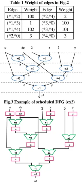
Fig.2 shows an example of operational unit binding graph of ex2 [10]. In Fig.2, *0, *1,*2,*3, and *4 are multipliers. Fig.2 represents the compatibility of these multipliers. Table 1 shows the weights of edges in Fig.2. The calculation for the weights of edges is explained as follows. Fig.3 shows the scheduled data flow graph (DFG) of ex2. In the DFG, each operation and each variable are assigned to an operational unit and a register with one-to-one, respectively. As the result of the assignments, the RTL datapath shown in Fig.4 is generated. Table 2 shows the input sequential depths and the output sequential depth of each multiplier in Fig.4. When *1 and *4 are merged to multiplier *1*4, the RTL datapath shown Fig.5 is generated. Table 3 shows the input sequential depths and the output sequential depth of each multiplier in Fig.5. Sequential depth of a merged operational unit becomes the minimum of those of two operational units. The left input sequential depth of *1 is infinity, the right input sequential depth of *1 is 1, the output sequential depth of *1 is 4, the left input sequential depth of *4 is 1, the right input sequential depth of *4 is 2, and the output sequential depth of *4 is 2 as shown in Table 2. Thus, the left input sequential depth of the merged *1*4 is 1, the right input sequential depth of *1*4 is 1, and the output sequential depth of *1*4 is 2 as shown in Table 3. Therefore, the weight of (*1, *4) is calculated as follows:
∑| sequential depth of *1 – sequential depth of *4|=|100- 1|+|1-2|+|4-2|=99+1+2=102.
Table 1 Weight of edges in Fig.2
Fig.3 Example of scheduled DFG (ex2)
Fig.4 RTL datapth after initial binding (ex2) Table 2 Sequential depth of each multiplier in Fig.4
D. Register binding graph
Our proposed method uses register binding graph G (V, E, w) for register binding. G is an undirected graph. In G, a vertex v (v∈V) represents a register. An edge (u, v) ((u, v)∈E, u, v∈V, u≠v) represents compatibility of registers u and v. Each edge has a weight w (w: E→Z+(Z+ is non-negative integers)). A weight w of edge (u, v) represents the sum total of reduction of input sequential depths and an output sequential depth of operational units when u and v are merged to a register.
Fig.5 RTL datapth after merging of *1 and *4 (ex2) Table 3 Sequential depth of each multiplier in Fig.5
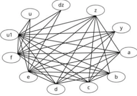
Fig.6 shows an example of register binding graph. In Fig.6, u, dz, z, y, a, b, c, d, e, f, and u1 are registers. Fig.6 represents the compatibility of these registers. Table 4 shows the weight of edges in Fig.6. This weight is calculated after operational unit binding using Fig.2 (*0, *3, and *4 are merged to same multiplier, *1 and *2 are merged to same multiplier). In Table 4, edges which have weight more than 1 are listed.
E. Weight-directed clique partitioning problem of operational unit binding graph
Input: An operational unit binding graph G Output: A result of operational unit binding Constraint: The number of operational units
Optimization: maximizing sum total of weight for edges which constitute each clique, i.e., sum total of reduction of input sequential depths and output sequential depths of all operational units.
F. Weight-directed clique pa rtitioning problem of register binding graph
Input: A register binding graph G Output: A result of register binding Constraint: The number of registers
Optimization: maximizing sum total of weight for edges which constitute each clique, i.e., sum total of reduction of input sequential depths and output sequential depths of all operational units.
u dz 3 z 5 y
*0 *1
*2 *3
-0 *4
-1 a b
c d
u1
e f
u dz
-0
-1
*0 *1
*2
*4
3 5
u1
z y
*3 a b
c d
u dz z y
e f
u1
Edge Weight Edge Weight (*1,*2) 100 (*2,*4) 2 (*1,*3) 1 (*3,*0) 100 (*1,*4) 102 (*3,*4) 101 (*2,*0) 3 (*4,*0) 3
left input right input output
*0 1 1 4
*1 ∞ 1 4
*2 2 2 3
*3 ∞ 1 3
*4 1 2 2
u dz
-0
-1
*0 *1*4
3 5
u1
y
*3 a b
d
u dz
y
e
u1 z z
*2 c
f
left input right input output
*0 1 1 4
*1*4 1 1 2
*2 2 2 3
*3 ∞ 1 3
III. PROPOSED ALGORITHM
Fig.7 shows our proposed binding algorithm to reduce input sequential depths and output sequential depths of operational units. Our binding algorithm can be applied for both of operational unit binding and register binding. In Fig.7, G is an operational unit binding graph or a register binding graph. BT is an upper limit of the number of backtracks. L is a constraint for the number of operational units or the number of registers. N is an upper limit of the number of edges which are inserted to a decision tree at one selection. In the algorithm, when vertex u and v are merged to new vertex w, w has information of u and v.
Line 2: the number of backtracks is initialized to 0.
Line 3: lines 4-27 are repeated while one or more edges exist in G.
Line 4: lines 5-15 are repeated while one or more edges exist in G.
Lines 5-8: if edge e which has only adjacent vertexes of degree ‘1’ exists in G, the adjacent vertexes of e are merged and G is updated.
Lines 9-15: if one or more edges exist in G, edge u which has maximum weight is selected. Next, N edges are gotten from the edge list which is sorted by descending order of weight, and the N edges are inserted into the decision tree. Finally, the adjacent vertexes of u are merged and G is updated.
Lines 17-18: if the number of vertexes in G is less than or equal to L, the vertex set of G is returned.
Lines 19-27: if the number of vertexes in G is more than L, the number of backtracks is incremented by 1. And if the number of backtracks is less than or equal to BT, backtrack is executed and G is updated. If the number of backtracks is more than BT, abort of search is returned.
Line 29: no solution is returned.
Fig.6 Example of register binding graph Table 4 Weight of edges in Fig.6
Fig.7 Proposed binding algorithm
IV. EXPERIMENTAL RESULTS
In this paper, we performed the experiments to evaluate the effectiveness of our proposed binding method. In the experiments, ex2 [10], ARF [11], BPF [11], and FFT [11] are used as experimental circuits. These circuits have constant value inputs. In the experiments, we synthesized RTL circuits by using our proposed binding method and Left-Edge Algorithm (LEA) [2], and compared the results of them. We used in-house ATPG tool “FTEM_ATPG” which can perform test generation using easily testable FTEMs [9]. We used Design Compiler from Synopsys for logic synthesis, and set bit widths of datapaths to 32. We evaluated single stuck-at faults in operational units. The evaluation items were “input sequential depths of operational units”, “output sequential depths of operational units”, “test generation time”, “fault coverage”, “test application time”, and “area of circuits”.
Table 5 shows the synthesis results of RTL circuits. In Table 5, “Circuit” column shows the name of circuits. “#Add”,
“Sub”, and “Mul” columns show the number of adders, the number of subtracters, and the number of multipliers, respectively. “Reg” column shows the number of registers.
“Mux” column shows the sum total of inputs of multiplexers.
“Area” column shows the area of whole circuits. “Area Overhead” column shows the area overhead of our proposed method. “#extra ST” column shows the number of extra state transitions inserted into RTL controller in the method [9]. Table 6 shows input sequential depths and output sequential depths of operational units. In Table 6, “Circuit” column shows the name of circuits. “OU” column shows the name of operational units. “Left” column shows the input sequential depths of left inputs of operational units. “Right” column shows the input sequential depths of right inputs of operational units. “Output” column shows the output sequential depths of operational units. In Table 6, our
Edge Weight Edge Weight Edge Weight Edge Weight
(b,u1) 1 (d,e) 1 (c,y) 2 (c,a) 1
(c,u1) 1 (d,f) 1 (d,u1) 2 (f,y) 2
(f,u1) 1 (c,u) 2 (c,b) 1 (f,a) 1
(a,u1) 2 (c,dz) 2 (f,u) 2 (f,b) 1
(a,e) 1 (c,z) 2 (f,dz) 2 (f,z) 2
(a,f) 1
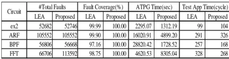
proposed method succeeded in reducing all input sequential depths and output sequential depths of operational units to 1. Table 7 shows the results of test generation. In Table 7,
“Circuit” column shows the name of circuits. “#Total Faults” column shows the number of target faults. “Fault Coverage” column shows the fault coverage. “ATPG Time” column shows the CPU time of test generation. “Test App Time” column shows the test application time.
In Table 7, our proposed method achieved higher fault coverage for all circuits compared to LEA. The fault coverage was improved by 1.04% on the average, and improved by 2.84% as the maximum. The test generation time was reduced by 10.70% on the average, and reduced by 94.00% as the maximum. The test application time was reduced by 9.00% on the average, and reduced by 34.63% as the maximum. This means that reducing input sequential depths and output sequential depths of operational units is effective for test generation using easily testable FTEMs. Especially, in FFT, input sequential depth ‘∞’ was reduced to 1. As a result, the fault coverage was improved. However, in Table 5, the area overhead of FFT is 51.86%. LEA synthesized operational units which have input sequential depth ‘∞ ’. These operational units are ones which have inputs of constant values. Generally, area of such an operational unit becomes small compared to normal operational unit. There were two multipliers with constant values and two subtracters with constant values in FFT generated by LEA. Therefore, the area overhead of FFT became large.
Table 5 Synthesis Results of RTL Circuits
Table 6 Input Sequential Depths and Output Sequential Depths of Operational Units
Circuit OU Left Right Output Circuit OU Left Right Output
MUL0 1 1 1 MUL0 1 1 1
MUL1 2 1 1 MUL1 1 1 1
SUB0 1 2 1 SUB0 1 1 1
MUL0 1 1 2 MUL0 1 1 1
MUL1 1 1 1 MUL1 1 1 1
MUL2 1 1 2 MUL2 1 1 1
MUL3 1 1 1 MUL3 1 1 1
ADD0 1 1 1 ADD0 1 1 1
ADD1 1 1 1 ADD1 1 1 1
MUL0 1 1 1 MUL0 1 1 1
MUL1 1 1 1 MUL1 1 1 1
SUB0 1 1 2 SUB0 1 1 1
SUB1 1 1 1 SUB1 1 1 1
ADD0 1 1 1 ADD0 1 1 1
ADD1 1 1 1 ADD1 1 1 1
MUL0 1 1 1 MUL0 1 1 1
MUL1 1 1 1 MUL1 1 1 1
MUL2 1 ∞ 1 MUL2 1 1 1
MUL3 1 ∞ 1 MUL3 1 1 1
ADD0 1 1 1 ADD0 1 1 1
ADD1 1 1 1 ADD1 1 1 1
ADD2 1 1 1 ADD2 1 1 1
ADD3 1 1 1 ADD3 1 1 1
SUB0 1 1 1 SUB0 1 1 1
SUB1 1 1 1 SUB1 1 1 1
SUB2 ∞ 1 1 SUB2 1 1 1
SUB3 ∞ 1 1 SUB3 1 1 1
FFT
ex2
ARF
BPF
FFT
LEA Our Proposed Method
ex2
ARF
BPF
Table 7 Results of Test Generation
LEA Proposed LEA Proposed LEA Proposed LEA Proposed ex2 52682 52746 99.99 100.00 2295.07 1312.19 99 104 ARF 105552 105552 99.90 100.00 16020.91 4899.20 291 326 BPF 56806 56668 97.16 100.00 28820.42 1728.52 257 168 FFT 66706 113592 98.75 100.00 4620.53 8305.04 328 268 Fault Coverage(%) ATPG Time(sec) Test App Time(cycle)
#Total Faults Circuit
V. CONCLUSION
This paper proposed input sequential depth and output sequential depth of operational units as testability measures. Furthermore, this paper proposed a binding method to reduce them. Our proposed method achieved higher fault coverage for all circuits compared to LEA. Future work includes performing experiments using larger DFG and CDFG circuits, and designing an algorithm which aims to reduce the number of extra state transitions inserted into RTL controller in controller augmentation [9].
Acknowledgments
This work was supported in part by Japan Society for the Promotion of Science (JSPS) under Grants-in-Aid for Science Research C (No.26330071).
#Add #Sub #Mul #Reg #Mux
ex2 0 1 2 5 7 16860 0 2
ARF 2 0 4 10 22 35984 0 2
BPF 2 2 2 8 18 21250 0 5
FFT 4 4 4 10 24 26579 0 4
#Add #Sub #Mul #Reg #Mux
ex2 0 1 2 5 10 17353 2.92 3
ARF 2 0 4 10 21 35754 -0.64 3
BPF 2 2 2 8 20 21800 2.59 3
FFT 4 4 4 10 34 40363 51.86 3
#Circuit Elements
#extra ST
#extra ST Our Proposed Method
LEA Circuit
Area OverHead (%)
Area OverHead (%) Area
Area Circuit #Circuit Elements
REFERENCES
[1] H. Fujiwara, Logic Testing and Design for Testability, The MIT Press, 1985.
[2] D. D. Gajski, N. D. Dutt, A. C-H Wu, and S. Y-L Lin, High-Level Synthesis: Introduction to Chip and System Design, Kluwer Academic Publishers, 1992.
[3] R. Nara, K. Satoh, M. Yanagisawa, T. Ohtsuki, and N. Togawa, “Scan- Based Side-Channel Attack Against RSA Crypto-Systems Using Scan Signatures,” IEICE Trans. on Fundamentals, Vol. E93-A, No. 12, pp2481-2489, 2010.
[4] M.T.-C. Lee, W. H. Wolf, and N. K. Jha, “Behavioral Synthesis for Easy Testability in Data Path Scheduling,” in Proc. Int. Conf. on Computer-Aided Design, pp.616 -619, 1992.
[5] M.T.-C. Lee, W. H. Wolf, and N. K. Jha, “Behavioral Synthesis for Easy Testability in Data Path Allocation,” in Proc. Int. Conf. Computer Design, pp. 29-32, 1992.
[6] M.T.-C. Lee, N. K. Jha, and W. H. Wolf, “Behavioral Synthesis for Highly Testable Datapaths Under the Non-Scan and Partial Scan Environments,” in Proc. Design Automation Conf., pp.292-297, 1993. [7] L.M.FLottes , B.Rouzeyre , L.Volpe,”A Controller reSynthesis Based
Methods For Improving Datapath Testability,” IEEE International Symposium on Circuits and Systems, pp. 347 -350, May 2000. [8] K. Sugiki, T. Hosokawa, and M.Yoshimura, ”A Test Generation
Method for Datapath Circuits Using Functional Time Expansion Models,” 14th IEEE Workshop on RTL and High Level Testing, pp.39- 44, Nov. 2008.
[9] T. Masuda, J. Nishimaki, T. Hosokawa, and H. Fujiwara, "A Test Generation Method for Datapaths Using Easily Testable Functional Time Expansion Models and Controller Augmentation," IEEE the 24th Asian Test Symposium, pp. 37-42, Nov. 2015.
[10] M.T.-C.Lee, High-Level Test Synthesis of Digital VLSI Circuits, Artech House Publishers, 1997.
[11] S. P. Mohanty, N. Ranganathan, E. Kougianos, and P. Patra, Low- Power High-Level Synthesis for Nanoscale CMOS Circuits”, Springer, 2008.