False Path Identification using RTL Information and
Its Application to Over-testing Reduction for Delay Faults
Yuki Yoshikawa
1, Satoshi Ohtake
2and Hideo Fujiwara
21
Graduate School of Information Science, Hiroshima City University
3-4-1 Ozuka-higashi, Asaminami, Hiroshima 731-3194, Japan
2
Graduate School of Information Science, Nara Institute of Science and Technology
Kansai Science City 630-0192, Japan
E-mail:
1[email protected],
2{ohtake, fujiwara}@is.naist.jp
Abstract
While design-for-testability (DFT) techniques are gen- erally used in order to reduce test generation complexity, they induce over-testing problems. In general, DFT tech- niques make a large number of untestable paths testable. However delay on the path that becomes testable does not affect circuit performance because the path was originally untestable. Therefore we consider testing such path to be over-testing. In this work, we reduce the over-testing by identifying false paths using register transfer level informa- tion. Our method identifies a subset of false paths within a reasonable time. Experimental results for some RTL bench- mark circuits show the effectiveness of our false path iden- tification method.
1. Introduction
Design-for-testability (DFT) techniques such as en- hanced scan [1] or standard scan with skewed-load test- ing [2] or broadside testing [3] are used to reduce test costs. These techniques make all or most of the sequen- tially untestable paths testable. However, delay on the path that becomes testable by some DFT never affect the cir- cuit performance. This is because no transition launched at the starting point of the untestable path is ever propa- gated to the ending point of the path during normal opera- tion. Therefore we consider testing such paths to be over- testing. The over-testing causes yield loss or overkill of products because good circuits in normal operations may be regarded as faulty ones under test mode. Moreover test generation time and test application time become shorter if the over-testing is reduced.
To reduce the over-testing, first, untestable paths in an original circuit should be identified. Then the information about the untestable paths should be propagated to the ac- tual test environment, that is, the paths that become testable by a DFT have to be excluded from testing. In the last decade, several path identification methods have been pro- posed. For combinational circuits, the techniques presented in [4, 5, 6] are approaches for identifying combinationally untestable paths at gate-level. The works for sequential cir- cuits [7, 8] are equally important. However, these gate- level approaches may be hard to handle all the exponential number of paths in large scale circuits. In [9], false paths are identified at RTL. However, their interest is to prevent an inaccurate decision about circuit performance caused by identifying false paths as critical paths. Hence they do not
list identified false paths and do not consider shorter false paths than critical paths.
As an approach from higher level, we propose a method of identifying false paths using RTL information such as load-enable signals of registers and select signals of mul- tiplexers (MUXs). In this paper, we first show a suffi- cient condition for identifying non-robust untestable paths. Then we also discuss extension of the condition for iden- tifying functionally unsensitizable (false) paths. We deal with paths at RTL, called RTL paths. An RTL path is a path which starts at a primary input or a register and ends at a register or a primary output, which passes through only combinational modules and has a bit width. The total num- ber of RTL paths in a circuit is much smaller than that of gate-level paths, therefore our path identification method can be performed in a reasonable amount of time. Experi- mental results for some RTL benchmark circuits show that our method can identify many RTL paths as false in a few seconds. In addition, we show that there are a lot of gate- level paths corresponding to the RTL paths that are identi- fied as false.
2. Preliminaries
2.1. RTL circuitOur path identification method approaches to structural RTL designs. A structural RTL design consists of a con- troller represented by a finite state machine and a datap- ath composed of RTL modules, which are MUXs, com- binational operation modules and registers, and RTL sig- nal lines between them. They are connected to each other by control signal lines and status signal lines. The con- troller controls control inputs of the RTL modules. We as- sume that all the control inputs of the RTL modules in the datapath are directly controlled by the controller. On the other hand, status signals from the datapath are fed into the controller. We assume that state transitions are completely specified for all pairs of a state and an input vector.
If a target RTL circuit is described as a functional RTL, it may be difficult to directly extract its structural RTL from the description. In such a case, we can obtain the informa- tion about structure during synthesis process.
2.2. Logic synthesis
Our path identification is applied to RTL paths in an RTL circuit and the information about the identified paths
IEEE 16th Asian Test Symposium (ATS'07), pp.65-68, October, 2007.
at RTL is propagated to gate-level paths in a gate-level cir- cuit transformed by logic synthesis. Then it is necessary to clarify the correspondence of RTL paths to gate-level paths. As one solution to achieve the clarification, we consider a restricted synthesis called module interface preserving- logic synthesis.
Definition 1:(Module interface preserving-logic synthe- sis)
Given an RTL circuit, if logic synthesis transforms each RTL module and each RTL signal line into an individual gate-level netlist and individual single-bit signal lines, re- spectively, the logic synthesis is referred to as module in- terface preserving-logic synthesis(MIP-LS). ✷ During an MIP-LS for an RTL circuit, optimization can only be performed within each module. Therefore, the con- nectivity of all the RTL modules is guaranteed to be prop- agated to a synthesized gate-level circuit through any MIP- LS.
3. False path identification
3.1. RTL false pathWe define an RTL false path as follows. Definition 2: (RTL false path)
An RTL path p in an RTL circuit is RTL false if any gate- level path corresponding to p in its gate-level circuit is gate- level false for any logic synthesis. ✷ Our objective is to identify bundles of gate-level paths as false by finding RTL false paths. However, it may be hard under any logic synthesis to map an RTL path to all the gate-level paths corresponding to the RTL path com- pletely. To achieve the mapping, we restrict logic synthesis to MIP-LS.
Definition 3: (RTL false path with respect to MIP-LS) An RTL path p in an RTL circuit is RTL false with respect to MIP-LSif any gate-level path corresponding to p in its gate-level circuit is gate-level false for any MIP-LS. ✷ In this paper, we focus on identification of RTL false paths w.r.t. MIP-LS. RTL false paths w.r.t. MIP-LS are just re- ferred to as RTL false paths in the rest of this paper. Theorem 1: An RTL path p in an RTL circuit is RTL false if at least one of the following three conditions is satisfied for any input sequence.
Condition 1: No transition is ever launched at the register of the starting point of p.
Condition 2:No transition at the starting point of p is ever propagated to the ending point along p.
Condition 3:No value captured into the register at the end- ing point of p is ever propagated to any primary output. ✷ If at least one of the three conditions of Theorem 1 is satisfied for any input sequence, any gate-level path cor- responding to p in a gate-level circuit synthesized by any MIP-LS is gate-level false. The proof is shown in [10]
3.2. Control-dependent false path
In this section, we show sufficiency of RTL false paths focusing on control signals of a controller. An RTL path identified by the sufficient condition is referred to as a control-dependent false path (CFP).
The state register (SR) in a controller represents states of the controller. We distinguish an RTL path starting at the
SR in a controller from the other RTL paths. By consider- ing state assignment, we can know the timing when transi- tions are launched for each bit of the SR and the directions of the transitions. Therefore we take the information about the state assignment and the directions of the transitions into account for identifying RTL false paths starting at the SR. A register in a datapath is referred to as a datapath reg- ister (DR).
RTL paths starting at DR/PI
Let P be a set of RTL paths that starts at a DR or a PI. Now we consider whether p ∈ P is a CFP or not. Let Rs and Re be the starting register and the ending register of p, respec- tively. Let CRs and CRe be load-enable signals of Rs and Re, respectively. If the load-enable signal of a register is equal to ’1’, the register loads a value; otherwise, it holds its value. Let Miand CMi (1 ≤ i ≤ n) be a MUX on p and its select signal, respectively, where n is the number of MUXs on p. Let CkM be the control value of M at time k. When Mi selects the input on p, the value of the select signal is denoted as pMi.
In the following discussion, we consider identification of non-robust untestable paths. Under single fault assump- tion (a single path is only affected by delay), the delay on a non-robust untestable path does not affect the cir- cuit performance. In this paper, a gate-level path is said to be false if the path is non-robust untestable. If we re- lax the single fault assumption, the delay on a non-robust untestable path may affect the circuit performance depend- ing on the delays on its off-paths. Our path identification method can also deal with functionally unsensitizable paths by simple extension of the sufficient condition for non- robust untestable.
We first consider uncontrollability and unobservability of registers. Then we show a sufficient condition for con- trol signals to identify RTL false paths in Lemma 1. Definition 4: (Uncontrollability of register R at time t) Let q be an RTL path whose ending register is R. For each state at time t − 1, if both of the following conditions are satisfied, R is uncontrollable at time t.
• For each q, control signal values of all the MUXs on qat time t and those at time t − 1 are the same.
• Each source register Rqof R is uncontrollable at time t− 1 or Ct−1R
q = 0, where a source register of R at time tis a register whose value affects R at time t. ✷ Definition 5: (Unobservability of register R at time t) Let r and Rr be an RTL path starting at R and its ending register, respectively. For each state at time t+ 1, if ev- ery r satisfies at least one of the following conditions, R is unobservable at time t.
• ∃i|1 ≤ i ≤ n,Ct+1M
i ̸= rMi, where n is the number of MUXs on r.
• Ct+1Rr = 0.
• Rr is unobservable at time t + 1. ✷ Lemma 1: An RTL path p is RTL false if at least one of the following three conditions is satisfied for any state tran- sition from time k to k+ 1.
Condition 1:(1) CRsk = 0 or (2) Rs is uncontrollable at time k.
Condition 2:∃i|1 ≤ i ≤ n,CMk+1
i ̸= pMi, where n is the num- ber of MUXs on p.
Condition 3:(1) Ck+1Re = 0 or (2) Re is unobservable at time
k+ 1. ✷
Lemma 1 is properly included in Theorem 1. The proof is shown in [10].
Any gate-level path corresponding to p is non-robust untestable if p is RTL false. The second condition of Lemma 1 means that at least one MUX on p does not se- lect p at time k+ 1. If the condition is extended such that at least one MUX on p does not select p at time k and k+ 1, any gate-level path corresponding to p is functionally un- sensitizable.
RTL paths starting at SR-ff
For RTL paths starting at flip-flops in the SR (SR-ff), Lemma 1 can also be applied. The SR in a controller up- loads a new value every clock cycle. It means that CRs
always becomes 1 (load). Therefore RTL paths from the SR-ff to DRs do not satisfy Condition 1 (1) of Lemma 1. Here we consider a transition at each SR-ff. The re- lation between each state and a value for each SR-ff is de- termined by state assignments. We can obtain the infor- mation on state assignments during logic synthesis or de- signers can also determine state assignments before logic synthesis. From the information on state assignments and state transition, we can know the timing when a transition is launched at each flip-flop.
An RTL path is false with respect to a rising (resp. falling) transition if at least one of the three conditions of Lemma 1 is satisfied for all the time t when a rising (resp. falling) transition launches at the SR-ff of the starting point of the RTL path.
3.3. Experimental results
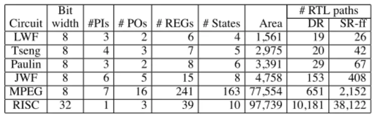
In this section, we evaluate the effectiveness of iden- tifying RTL false paths as control-dependent false paths (CFPs). The circuit characteristics of RTL benchmarks are shown in Table 1. LWF, Tseng, Paulin and JWF are widely used benchmark circuits. MPEG and RISC1are more prac- tical and larger circuits provided by industry. Each cir- cuit consists of a controller and a datapath. The first eight columns show circuit name, the bit width of the datapath, the numbers of the PIs, the POs, the registers and the states in the controller, and the total area of the circuit, respec- tively. Logic synthesis was performed by DesignCompiler (Synopsys). The last two columns show the number of RTL paths. Columns DR and SR-ff show the number of RTL paths where an RTL path starts at a datapath register or a PI and the number of RTL paths where an RTL path starts at an FF in the SR, respectively.
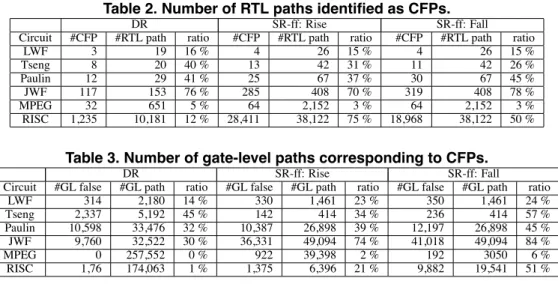
Table 2 shows the results for the number of RTL paths identified as CFPs. The second, third and fourth columns under DR show the number of RTL paths identified as CFPs starting at DR, the number of RTL paths starting at DRs, and the ratio of the number of CFPs to that of RTL paths, respectively. For LWF, Tseng, Paulin, JWF and MPEG, CPU times required for identifying CFPs were less than 1 second. For JWF circuit, many RTL paths (117 of 153) were identified as CFPs. MPEG has many registers with no hold function. Therefore, many starting registers launch transitions and many ending registers capture the propa- gated transitions every clock cycle. Hence the number of CFPs is small. For RISC, the CPU time required for identi- fying 1,235 CFPs of 10,181 RTL paths is about 10 seconds.
1These circuits were provided for the Joint Research (1997-2001) with Semiconductor Technology Academic Research Center (STARC).
Table 1. Characteristics of benchmarks.
Bit # RTL paths
Circuit width #PIs # POs # REGs # States Area DR SR-ff
LWF 8 3 2 6 4 1,561 19 26
Tseng 8 4 3 7 5 2,975 20 42
Paulin 8 3 2 8 6 3,391 29 67
JWF 8 6 5 15 8 4,758 153 408
MPEG 8 7 16 241 163 77,554 651 2,152
RISC 32 1 3 39 10 97,739 10,181 38,122
The next three columns and the last three columns show re- sults for RTL paths starting at SR-ffs with rising transitions and starting at SR-ffs with falling transitions, respectively. For all the circuits except for RISC, the ratios of RTL paths identified as CFPs are similar to those of RTL paths start- ing at DRs. For RISC, a large number of RTL paths are identified.
Table 3 shows the result of gate-level false paths corre- sponding to RTL paths identified as CFPs. We extracted gate-level paths from the longest path, which has larger propagation delay, by using the “report path” function of the timing analysis tool Prime Time (Synopsys). For LWF, Tseng, Paulin and JWF, we extract all the paths in each cir- cuit. For MPEG and RISC, we extract 300,000 and 200,000 gate-level paths from the longest path, respectively. The second column shows the number of gate-level paths cor- responding to CFPs. We can say that these gate-level false paths were identified by our method. The third column shows the total number of gate-level paths starting at DRs. The fourth column shows the ratio of the second column to the third column. For Paulin, our method identified 10,598 of 33,476 (32%) gate- level paths as false paths within 1 second. We perform sequential test generation (TetraMax, Synopsys) for only 100 paths in Paulin, then it took 498 second to identify 51 paths as untestable. If an RTL path that passes a large scale operational module such as a mul- tiplier is identified as a CFP, a large number of gate-level paths are identified as false paths. For MPEG, most of the extracted 300,000 paths start at DRs. Gate-level paths corresponding to CFPs starting at DRs were not included among the extracted paths. One reason is that gate-level paths corresponding to the identified CFPs have short prop- agation delays, hence they were not included among the ex- tracted paths. As another reason, MPEG may have a small number of false paths.
4. Reduction in Over-testing
To reduce over-testing, we consider that PDFs on paths identified as false are excluded from a fault list targeted by test generation, and then test generation is performed for the fault list. However, during test application, pat- terns generated by the test generation may still detect the excluded faults accidentally. This is because a generated pattern to detect some PDF in the fault list may also acti- vate other PDFs simultaneously. In this work, we evaluate such circumstance. In this experiment, we adopt an en- hanced scan technique as a DFT method. Table 4 shows the results of over-tested PDFs for each benchmark circuit. Fault lists are generated by using the “write path” function of Prime Time. The second column shows the total num- ber of PDFs. The third column shows the number of PDFs on CFPs. We generate test patterns for fault lists exclud- ing PDFs on CFPs, then perform fault simulation for fault
Table 2. Number of RTL paths identified as CFPs.
DR SR-ff: Rise SR-ff: Fall
Circuit #CFP #RTL path ratio #CFP #RTL path ratio #CFP #RTL path ratio
LWF 3 19 16 % 4 26 15 % 4 26 15 %
Tseng 8 20 40 % 13 42 31 % 11 42 26 %
Paulin 12 29 41 % 25 67 37 % 30 67 45 %
JWF 117 153 76 % 285 408 70 % 319 408 78 %
MPEG 32 651 5 % 64 2,152 3 % 64 2,152 3 %
RISC 1,235 10,181 12 % 28,411 38,122 75 % 18,968 38,122 50 %
Table 3. Number of gate-level paths corresponding to CFPs.
DR SR-ff: Rise SR-ff: Fall
Circuit #GL false #GL path ratio #GL false #GL path ratio #GL false #GL path ratio
LWF 314 2,180 14 % 330 1,461 23 % 350 1,461 24 %
Tseng 2,337 5,192 45 % 142 414 34 % 236 414 57 %
Paulin 10,598 33,476 32 % 10,387 26,898 39 % 12,197 26,898 45 %
JWF 9,760 32,522 30 % 36,331 49,094 74 % 41,018 49,094 84 %
MPEG 0 257,552 0 % 922 39,398 2 % 192 3050 6 %
RISC 1,76 174,063 1 % 1,375 6,396 21 % 9,882 19,541 51 %
Table 4. Number of over-tested PDFs.
Circuit Total #PDFs #PDFs on CFPs #Over-tested PDFs
LWF 3,598 619 392 (63%)
Tseng 5,868 2,928 1,185 (40%)
Paulin 37,171 19,477 2,195 (11%)
JWF 45,658 37,150 3,452 (9%)
MPEG 41,521 340 220 (65%)
RISC 25,496 6,974 509 (7.3%)
lists including the total PDFs. The fourth column shows the number of tested PDFs among PDFs shown in the third col- umn. Our experimental results show that 10-60% of the re- moved PDFs is accidentally tested (over-tested) if we gen- erate two-pattern tests with no input constraint.
To avoid the over-testing, we use constrained two- pattern tests called single-port-change (SPC) two-pattern tests[11]. The concept of SPC two-pattern tests was origi- nally proposed by authors to reduce area overhead required for DFTs compared to that required for DFTs by our previ- ous work[12]. We can utilize the concept for avoiding the over-testing completely. An SPC two-pattern test changes the second vector at only one port and sets stable for the other ports. Here a port means an output of a register, and it has bit width. An SPC two-pattern test can test PDFs on paths starting at the port whose second vectors are changed. With respect to test quality, SPC two-pattern tests guaran- tee robust (resp. non-robust) test for a PDF if the PDF is ro- bust (resp. non-robust) testable[11]. In terms of reduction in over-testing, when SPC two-pattern tests are generated for fault lists excluding PDFs corresponding to CFPs, the removed PDFs are never tested.
5. Conclusion
In this paper, we have introduced a concept of register- transfer level (RTL) false paths and proposed a method of identifying them. Our experimental results showed that a large number of gate-level false paths were found by identi- fying RTL false paths. Time required for the identification was much shorter than that for the identification at gate- level. To reduce over-testing, path delay faults (PDFs) on the identified false paths are excluded from the fault list targeted by test generation. However even if the PDFs are removed from the fault list, the generated test patterns incidentally test the removed faults. Therefore, we have also proposed a method to avoid over-testing by generating
single-port-change two-pattern tests. In the experimental results, we showed that 10-60% of removed PDFs is over- tested if we normally generate unconstrained two-pattern tests.
Acknowledgment
The authors would like to thank Profs. Michiko Inoue and Tomokazu Yoneda of Nara Institute of Science and Tech- nology for their valuable discussion and their cooperation. This work was supported in part by Semiconductor Tech- nology Academic Research Center (STARC) under the Re- search Project, in part by 21st Century Center of Excel- lence (COE) Program (Ubiquitous Networked Media Com- puting), and in part by Japan Society for the Promotion of Science (JSPS) for Young Scientists (B) (No.17700062).
References
[1] B.I. Devadas and G.E. Stong, “Design for testability using scanpath techniques for path delay test and measurement,” Proceeding of In- ternational Test Conf., pp.365–374, 1991.
[2] J. Savir and S. Patel, “Scan-based transition test,” IEEE Trans. on CAD, vol.12, no.8, pp.1232–1241, Aug. 1993.
[3] J. Savir and S. Patel, “Broad-side delay test,” IEEE Trans. on CAD, vol.13, no.8, pp.1057–1064, Aug. 1994.
[4] K.T. Cheng and H.C. Chen, “Classification and identification of non- robust untestable path delay faults,” IEEE Trans. Computer-Aided Design of Integrated Circuits and Systems, vol.15, no.8, pp.854– 853, Aug. 1996.
[5] S. Kajihara, K. Kinoshita, I. Pomeranz, and S.M. Reddy, “A method for identifying robust dependent and functionally unsensitizable paths,” Proc. Int. Conf. on VLSI Design, pp.82–87, 1997. [6] S.M. Reddy, S. Kajihara, and I. Pomeranz, “An efficient method
to identify untestable path delay faults,” IEEE the 10th Asian test symposium, pp.233–238, Nov. 2001.
[7] A. Krstic, S.T. Chakradhar, and K.T. Cheng, “Testable path delay fault cover for sequential circuits,” Proc. European Design Automa- tion Conference, pp.220–226, Sep. 1996.
[8] R. Tekumalla and P.R. Menon, “Identifying redundant path delay faults in sequential circuits,” Proc. 9th International Conf. VLSI De- sign, pp.406–411, Jan 1996.
[9] M. Nourani and A. Papachristou, “False path exclusion in delay analysis of RTL structures,” IEEE Trans on VLSI Systems, vol.10, no.1, pp.30–43, Feb. 2002.
[10] Y. Yoshikawa, S. Ohtake, and H. Fujiwara, “Over-testing reduction for delay faults through false paths exclusion using RTL informa- tion,” NAIST Information Science Technical Report, NAIST-IS-TR 2007012, June 2007.
[11] Y. Yoshikawa, S. Ohtake, M. Inoue, and H. Fujiwara, “Design for testability based on single-port-change delay testing for data paths,” IEEE the 14th Asian Test Symposium, pp.254–259, Dec. 2005. [12] M.A. Amin, S. Ohtake, and H. Fujiwara, “Design for hierarchical
two-pattern testability of data paths,” IEEE the 10th Asian test sym- posium, pp.11–16, Nov. 2001.