Single-Control Testability of RTL Data Paths for BIST
Toshimitsu Masuzawa Minoru Izutsu Hiroki Wada
Hideo Fujiwara
Graduate School of Information Science
Nara Institute of Science and Technology
8916-5 Takayama, Ikoma, Nara, 630-0101, Japan
masuzawa,hiroki-w,fujiwara @is.aist-nara.ac.jp
Abstract
This paper presents a new BIST method for RTL data paths based on single-control testability, a new concept of testability. The BIST method adopts hierarchical test. Test pattern generators are placed only on primary inputs and test patterns are propagated to and fed into each module. Test responses are similarly propagated to response analyz- ers placed only on primary outputs. For the propagation of test patterns and test responses, paths existing in the data path are utilized. The DFT method for the single-control testability is also proposed.
The advantages of the proposed method are high fault coverage (for single stuck-at faults), low hardware over- head and capability of at-speed test. Moreover, test patterns generated by test pattern generators can be fed into each module at consecutive system clocks, and thus, the BIST can also detect some faults of other fault models (e.g., transition faults and delay faults) that require consecutive application of test patterns at speed of system clock.
1 Introduction
Built-in self-test (BIST) is one of the most important techniques for testing large and complex VLSI circuits. In this technique, test pattern generators (TPGs) are added to primary inputs (PIs) and response analyzers (RAs) are added to primary outputs (POs). However, adding these TPGs and RAs is not sufficient to achieve high fault cover- age (for single stuck-at faults), if the VLSI circuit contains cycles in its structure. Thus, several techniques of design for testability (DFT) have been proposed[1].
BIST methods are classified into test-per-scan scheme and test-per-clock scheme. In the test-per-scan scheme, (some) registers are modified into scan registers so that test
The author is currently with Software Division, Hitachi, Ltd.
patterns and test responses can be shifted into and out using a scan path. A major drawback of this scheme is long test application time caused by the scan. Another major draw- back is difficulty in applying test patterns at the operational speed of the circuits (at-speed test). At-speed test is impor- tant since it can detect more defective circuits than the same test sequence applied at a lower rate in scan mode[6].
In the test-per-clock scheme, some registers are en- hanced so that they can generate test patterns and/or com- pact test responses. Examples of these registers are BILBO (built-in logic block observer)[5] and CBILBO (concurrent BILBO). The advantages of this scheme is that at-speed test is possible and thus test application time is short. However, the test-per-clock scheme generally requires higher hard- ware overhead than the test-per-scan scheme.
Stroele and Wunderlich [8] proposed a DFT method for BIST of the test-per-clock scheme. The DFT method mod- ifies a data path so that every cycle in the data path contains at least two BILBOs or one CBILBO.
In this paper, we consider BIST of register-transfer-level (RTL) data paths. We introduce a new concept, single- control testabilityof a data path, that guarantees high fault coverage by BIST of the test-per-clock scheme. The BIST is based on hierarchical test: each combinational module (i.e., an operational module or a multiplexor) is tested in- dependently from other modules. The single-control testa- bility guarantees that, for each combinational module, test patterns generated by TPGs can be fed into the module at consecutive system clocks and its test responses can be con- secutively propagated to an RA. In other words, we can realize a configuration equivalent to that where TPGs are placed immediately before the inputs of the module and an RA is placed immediately after the output of the mod- ule. Thus, the single-control testability guarantees high fault coverage (for single stuck-at faults) since most of com- binational modules in actual data paths are random-pattern testable or can be modified into random-pattern testable one by adequate test point insertion[2]. Moreover, the BIST can
IEEE the 9th Asian Test Symposium (ATS 2000), pp. 210-215, Dec. 2000.
also detect some faults of other fault models (e.g., transition faults and delay faults) that require consecutive application of test patterns at speed of system clock.
We also present a DFT method for modifying a data path to a single-control testable one with low hardware overhead. To reduce the hardware overhead, the DFT method adds TPGs and RAs on only PIs and POs. To guarantee prop- agation of test patterns and test responses, some operational modules are augmented with thru function and some multi- plexors are added.
The advantages of our BIST are summarized as follows. high fault coverage
low hardware overhead
At-speed test is possible. Moreover, test patterns gen- erated by TPGs can be applied to each module at con- secutive system clocks.
The paper is organized as follows. In Section 2, we intro- duce a data path and its graph model. Section 3 introduces the single-control testability. Section 4 presents the DFT method for the single-control testability. We present exper- imental results in Section 5 and the conclusions in Section 6.
2 Data Path
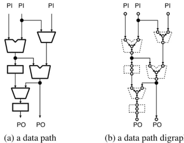
A data path consists of hardware elements and lines. A hardware element is a primary input (PI), a primary out- put (PO), a register, a multiplexor (MUX), or an opera- tional module. An operational module is a combinational circuit and includes no register. In the rest of this paper, operational modules and MUXs are simply called (combi- national) modules. We introduce ports as interface points of each hardware element in a natural fashion: values en- ter into a hardware element through its input ports, and exit through its output port. For convenience, we regard a PI (resp. a PO) as an output port (resp. an input port). A line connects an output port with an input port. Any number of lines can connect to an output port (i.e., fanout is allowed), but only one line can connect to an input port.
We use a data path digraph to represent structure of a data path:
where
is the set of all hardware elements in the data path, and
is the set of all ports in the data path. where
output port is con- nected to input port by a line ,
is an input port of , and
is an output port of .
PO
PI PI PI
PO PO
PI PI PI
PO
(a) a data path (b) a data path digraph Figure 1. A data path and its data path digraph
Figure 1 illustrates a data path and its data path digraph. This figure also demonstrates the correspondence between a data path and its data path digraph.
We use some graph terms (e.g., path, cycle etc.) to a data path digraph. We also use the graph terms to a data path, since there is a straightforward correspondence between a data path and its data path digraph.
The data paths considered in this paper are fairly general and satisfy most of the standard assumptions applicable to data path designs. We assume that all input and output ports have the same bit width. We also assume, for simplicity, that each module has exactly two input ports and only one output port.
Further, a hardware element may have a control port to feed control signals in and/or a status port to report results to the controller.
3 Single-Control Testability
Most of modules (e.g., adders, subtracters, multipliers, shifters and multiplexors) in actual data paths are random- pattern testable and other modules (e.g., comparators) not random-pattern testable can be changed into random- pattern testable ones by adequate test point insertion[2]. Thus, we can achieve high fault coverage of the whole data path by BIST if random test patterns generated by TPGs are propagated to each module and its test responses are propagated to an RA. We formalize this condition as single- control testabilityof a data path.
Definition 1 A data path is single-control testable if there exist three disjoint paths , and for each module such that
(a) any value can be propagated along each of and ,
(b) each of and is a path from a TPG to an input port of (remark that, from disjointness requirement, the TPGs and the input ports of and are respectively different from each other), and
(c) is a path from the output port of to an RA. Paths and are referred to as control paths of and is referred to as an observation path of .
The BIST method proposed in this paper is based on hi- erarchical test: each module is tested independently from other modules. The single-control testability guarantees that, for each module, test patterns generated by TPGs can be propagated to the module at consecutive system clocks using the control paths and and its test responses can be consecutively propagated to an RA using the observation path .
During test of each module , modules on and are controlled by a BIST controller so that random test patterns and test responses of can be propagated along these paths. Since these paths are mutually disjoint, the con- trol for the modules is fixed during test of . Thus, we refer to the condition of Definition 1 as single-control testability. The single-control testability implies testability with BIST, while it is closely related to weak testability[9], strong testability[10] and fixed-control testability[7] intro- duced for testability with external test.
4 DFT for Single-Control Testability
This section presents a design for testability (DFT) method that transforms a given data path to a single-control testable one. In the DFT, TPGs and RAs have to be added to the given data path. To reduce hardware overhead, we impose a restriction on addition of TPGs and RAs: TPGs and RAs can be added only on primary inputs and outputs respectively. The only exception of the restriction is addi- tion of a TPG for a data path with a single PI. In the rest of this paper, we consider the DFT under the restriction. 4.1 Problem Formulation
A single-control testable data path has two control and one observation paths for each module . These path are disjoint and can propagate any value along each of them. When a given data path does not have such disjoint paths for a module, paths are added using test MUXs in the proposed DFT. Each operational module appearing on the paths has to propagate any value on its input port to the output port. For the propagation, we augment the module with thru function if necessary. The test MUXs and the thru functions added in the DFT is referred as the DFT elements.
Definition 2 The DFT for the single-control testability is formalized as the following optimization problem.
Input: a data path
Output: a single-control testable data path
Optimization: minimizing hardware overhead (i.e., hardware of added DFT elements)
4.2 DFT algorithm
We propose a DFT algorithm for the single-control testa- bility. The algorithm consists of the following two stages. Stage 1 For each module, determine the control paths and
add the DFT elements for the paths.
Stage 2 For each module, determine the observation path and add the DFT elements for the paths.
We consider the control paths and the observation path separately since determining whether or not there exist these disjoint paths for a module is regarded as a NP- complete problem, the multicommodity flow problem[4]. 4.2.1 DFT for Control Paths (Stage 1)
The objective of the first stage is to modify a given data path with the minimum hardware overhead so that each mod- ule has two disjoint control paths. The DFT algorithm pro- cesses modules one by one: for each combinational module, it determines the control paths that can be realized with the minimum hardware overhead and adds the DFT elements for the paths.
The whole hardware overhead differs depending on the order of adding the DFT elements (i.e., the order of the modules processed) since the DFT elements added for for- mer modules can be utilized for a later one. Thus, the order of adding the DFT elements is very important to minimize the whole hardware overhead. The strategy of the algorithm is that it first adds the necessary DFT elements that have no alternatives (Step 1), and then adds the DFT elements in descending order of usability (Step 2). We present more details of each step in the following.
Step 1: Preprocess
The necessary DFT elements with no alternatives are added as follows.
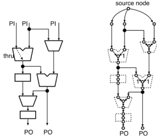
1. If the data path has only a single TPG (i.e., PI), it is clear that no module has two disjoint control paths. Thus, a TPG is added (Fig. 2 (a)). (Recall that this is the only exception of TPG addition.)
2. Each module is checked whether its two input ports are connected from the same module through only reg- isters. In this case, it is clear that does not have two disjoint control paths. Thus, we add a direct path from a TPG to an input port of as in Fig. 2 (b). If the other input port of is reachable from only one TPG, then another TPG is chosen to be connected with the test MUX. This guarantees that has two disjoint control paths. Otherwise, any TPG can be chosen.
PO PI TPG
PO PI
PO PI PI
M
PO PI PI
M
(a) TPG insertion (b) test MUX insertion Figure 2. Preprocess
Step 2: Determination of the control paths
Modules are checked one by one to determine the con- trol paths and the DFT elements for the control paths are added. To minimize the whole hardware overhead, the al- gorithm tries to add the DFT elements in descending order of usability.
In what follows, we first show how the control paths of a module are determined and then briefly show the order of the modules processed.
Determination of control paths
Control paths of module are determined by solving the minimum cost flow problem as follows.
1. Add a source node to the data path digraph and add arc for each TPG (i.e., PI) .
2. Let be the sink node .
3. For each arc in the resultant graph, we define its capacity and define its cost as follows.
if is an input port of module . otherwise.
( is the hardware cost of thru function from to the output port of . if the thru function is added in process of former modules.)
4. Find the minimum cost integral flow of flow value 2. (Flow cost is the sum of arc costs over all arcs with flow of value 1.) The paths of the minimum cost flow are determined as the control paths of .
The digraph may not have flow of value 2 for module . This implies that there exist no disjoint control paths for , thus, a direct path from a TPG to is added by a similar way in the preprocess (Fig. 2(b)).
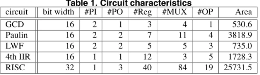
Figure 3 shows an example of the digraph for the mini- mum cost flow problem. In this figure, the hardware cost of thru function is 1.
Order of modules processed
To minimize the whole hardware overhead, it is desired that the DFT elements are added in descending order of
thru
PO PO
1
1 1
PO
PI PI PI
PO
source node
Figure 3. A digraph for the minimum cost flow problem
usability. Thus, in the DFT algorithm, modules nearer to TPGs are processed earlier in principle. This is because such modules have fewer choice of control paths and be- cause the DFT elements nearer to the TPGs has high us- ability, that is, descendant modules can utilize the DFT el- ements. To reduce hardware overhead, we use some aux- iliary heuristics to determine the order, however, we omit further details in this paper.
4.3 DFT for Observation Paths (Stage 2)
The objective of the second stage is to modify the data path with the minimum hardware overhead so that each module has an observation path disjoint from its control paths. The proposed algorithm processes modules one by one: for each module, it determines the observation path that can be realized with the minimum hardware overhead and adds the DFT elements for the path.
The observation path of module is determined by a similar way to that for the control paths.
1. Add a sink node to the data path digraph and add arc for each RA (i.e., PO) .
2. Let be the source node .
3. Remove the arcs and nodes that appear on the control paths of .
4. Define the capacity and cost of each arc in the same way as that for the control paths.
5. Find the minimum cost integral flow of flow value 1 (i.e., the minimum cost path). The path of the mini- mum cost flow is determined as the observation path of .
The digraph may have no path from to an RA. This implies that there exists no observation path for that is
Table 1. Circuit characteristics
circuit bit width #PI #PO #Reg #MUX #OP Area
GCD 16 2 1 3 4 1 530.6
Paulin 16 2 2 7 11 4 3818.9
LWF 16 2 2 5 5 3 735.0
4th IIR 16 1 1 12 3 5 1728.3
RISC 32 1 3 40 84 19 25731.5
Table 2. Hardware overheads(HWOH)
DFT method in [8] our DFT method
circuit bit width HWOH(%) #BILBO #CBILBO HWOH(%) #MUX #THRU #LFSR
8 89.30 18.67
GCD 16 74.54 1 1 18.36 1 1 0
32 66.67 18.06
8 80.74 22.50
Paulin 16 40.25 0 6 13.23 8 5 0
32 20.07 7.27
8 43.23 35.10
LWF 16 34.86 0 1 33.32 4 3 0
32 30.87 32.47
8 41.47 33.73
4th IIR 16 29.65 0 2 27.02 5 6 1
32 25.70 25.10
RISC 32 59.12 0 33 18.42 36 18 1
disjoint from its control paths, thus, a direct path from to an RA is added using a test MUX.
To minimize the whole hardware overhead, it is desired that the DFT elements are added in descending order of us- ability. Thus, in the DFT algorithm, modules nearer to RAs are processed earlier by the same reason as that for the con- trol paths. For lack of space, we omit further details.
5 Experimental results
In this section, we present experimental results of the proposed method. We applied the method to four bench- marks (a greatest common divisor (GCD), Paulin[3], 3rd Lattice Wave Filter (LWF) and 4th order IIR cascade filter (4th IIR)) and a RISC processor provided by industry.
Table 1 shows the characteristics of these data paths. Columns #PI, #PO, #Reg, #MUX and #OP denote the num- bers of PIs, POs, registers, MUXs and operational modules respectively. Column Area denotes the gate equivalents of the circuits synthesized by AutoLogicII (Mentor Graphics) using the logic synthesis library provided by ALTERA.
Table 2 shows the hardware overhead (HWOH). To eval- uate the effectiveness of our DFT method, we compare it with the DFT method proposed in [8]. For the DFT method
in [8], columns #BILBO and #CBILBO denote the numbers of registers modified into BILBOs and CBILBOs respec- tively. For our DFT method, columns #MUX and #THRU denote the numbers of added test MUXs and added thru functions respectively. Column #LFSR denote the number of LFSRs (linear-feedback shift registers) added as TPGs (recall the preprocess of the DFT for the control paths). No- tice that the hardware overhead in this table does not contain that for TPGs and SAs added at PIs and POs since these are usually added in any BIST method.
From the experimental results, we can see that our DFT is superior in the hardware overhead.
Table 3 shows the final fault coverage (FC) and the num- bers of clock cycles to attain the fault coverage1. These are estimated for single stuck-at faults by the fault simulator of TestGen (Synopsys). In all benchmarks, our DFT method achieves higher fault coverage than the DFT method in [8]. This is because each target of hierarchical test is smaller in our method: our method tests each module one by one while the method in [8] tests each acyclic sub-circuit. It is useful to mention that all of the faults that are not detected by our DFT method are proved to be either undetectable or
1We cannot estimate fault coverage for the RISC processor because of its large circuit size.
Table 3. Fault coverage and test application time DFT in [8] Our DFT method circuit
FC (%) #clock FC (%) #clock
GCD 96.07 556 99.83 10178
Paulin 99.84 1108 99.89 20531
LWF 81.44 143 99.82 554
4th IIR 97.89 136 99.57 604
detectable only by the pattern.
6 Conclusions
This paper proposed a new BIST method for RTL data paths. The advantages of the method are high fault cover- age, low hardware overhead and capability of at-speed test. Moreover, test patterns generated by TPGs can be applied to each module at consecutive system clocks.
This paper introduced a new concept of testability, the single-control testability, to characterize a data path that the proposed BIST can be applied to. The DFT method that transforms a data path into single-control testable one was also proposed and its advantages were proved by experi- mental results.
One of our future works is to introduce concurrent BIST to reduce test application time.
Acknowledgments
This work was supported in part by Semiconductor Tech- nology Academic Research Center (STARC) under the Re- search Project, by Japan Society for the Promotion of Sci- ence (JSPS) under the Grant-in-Aid for Scientific Research, and by Foundation of Nara Institute of Science and Technol- ogy under the Grant for Activity of Education and Research. Authors would like to thank Tomoo Inoue (Hiroshima City University), Michiko Inoue and Satoshi Ohtake (Nara Insti- tute of Science and Technology).
References
[1] M. Abramovici, M. A. Breuer, and A.D.Friedma: Digital Sys- tems Testing and Testable Design, Computer Science Press (1990).
[2] I. Ghosh, N. K. Jha, and S. Bhawmik: “A BIST scheme for RTL controller-data paths based on symbolic testability anal- ysis,” In Proc. Design Automation Conf., pp. 554–559 (1998). [3] I. Ghosh, A. Raghunathan, and N. K. Jha: “Design for hi- erarchical testability of RTL circuits obtained by behavioral synthesis,” In Proc. IEEE Int. Conf. on Computer Design, pp. 173–179 (1995).
[4] M. R. Garey, D. S.Johnson: Computers and Intractability: A Guide to the Theory of NP-Completeness, W. H. Freeman (1979).
[5] B. Koenemann, J. Mucha, and G. Zwiehoff: “Built-in logic block observation techniques,” In Proc. IEEE Test Conf., pp. 37–41 (1979).
[6] P. C. Maxwell, R. C. Aitken, V. Johnson, and I. Chiang: “The effect of different test sets on quality level prediction: When is 80% better than 90%?” In Proc. Int. Test Conf., pp. 358–364 (1991).
[7] S. Nagai, H. Wada, S. Ohtake, and H. Fujiwara: “A non- scan DFT method for RTL circuits based on fixed-control testability (in Japanese),” Technical Report VLD99-101 (also CPSY99-110), IEICE (2000).
[8] A. P. Stroele and H. J. Wunderlich: “Hardware-optimal test register insertion,” IEEE Trans. on Computer-Aided Design of Integrated Circuits and Systems, 17(6):531–539 (1998). [9] K. Takabatake, M. Inoue, T. Masuzawa, and H. Fujiwara:
“Non-scan design for testable data paths using thru opera- tion,” In Proc. Asia and South Pacific Design Automation Conf., pp. 313–318 (1997).
[10] H. Wada, T. Masuzawa, K. K. Saluja, and H. Fujiwara: “De- sign for strong testability of RTL data paths to provide com- plete fault efficiency,” In Proc. Int. Conf. on VLSI Design., pp. 300–305 (2000).
![Table 3. Fault coverage and test application time DFT in [8] Our DFT method circuit FC (%) #clock FC (%) #clock GCD 96.07 556 99.83 10178 Paulin 99.84 1108 99.89 20531 LWF 81.44 143 99.82 554 4th IIR 97.89 136 99.57 604](https://thumb-ap.123doks.com/thumbv2/123deta/5753320.27125/6.918.288.603.139.264/table-fault-coverage-application-method-circuit-clock-paulin.webp)
