A DFT Method for Time Expansion Model at Register
Transfer Level
Hiroyuki Iwata Tomokazu Yoneda Hideo Fujiwara
Graduate School of Information Science, Nara Institute of Science and TechnologyKansai Science City 630-0192, Japan {
hiroyu-i,yoneda,fujiwara
}@is.naist.jp
ABSTRACT
This paper presents a non-scan design-for-testability method for register transfer level circuits. We first introduce a new testability of RTL circuits called partially strong testability. The partially strong testability guarantees that the number of time frames required for any testable fault is bounded by a linear function of the number of registers in the RTL circuit during test generation process. We also propose a DFT method to make RTL circuits partially strongly testable. Experimental results show that we can reduce hardware overhead and test application time drastically compared to the pre- vious methods. Moreover, the proposed method can achieve 100% fault efficiency in practical test generation time and allow at-speed testing.
Categories and Subject Descriptors
B.8.1 [Performance and Reliability]: Reliability, testing and fault tolerance
General Terms
Design, Reliability
Keywords
design-for-testability, register transfer level, at-speed testing
1. INTRODUCTION
With the progress of semiconductor technology, testing of VLSI becomes more difficult and the cost is increasing. Therefore, it is important to achieve high fault efficiency (FE) with low cost. For combinational circuits, test patterns with 100% FE can be obtained by automatic test pattern generators (ATPGs). For sequential cir- cuits, the test generation can be modeled by iterative combinational arrays so that combinational test generation methods can be used. Test generation for sequential circuits is more complex than that for combinational circuits because of the number of time frames needed for the justification and the error propagation. In the worst case, the number of time frames is the exponential function of the number of flip-flops (FFs). For acyclic sequential circuits, how- ever, it is known that test patterns with 100% FE can be obtained
Permission to make digital or hard copies of all or part of this work for personal or classroom use is granted without fee provided that copies are not made or distributed for profit or commercial advantage and that copies bear this notice and the full citation on the first page. To copy otherwise, to republish, to post on servers or to redistribute to lists, requires prior specific permission and/or a fee.
DAC 2007,June 4–8, 2007, San Diego, California, USA. Copyright 2007 ACM ACM 978-1-59593-627-1/07/0006 ...$5.00.
in practical test generation time [1]. To ease the complexity of the test generation, design-for-testability (DFT) techniques have been proposed.
The most widely used DFT technique for sequential circuits is the full scan approach. In the full scan approach, test generation algorithm for combinational circuits can be applied. Therefore, this approach can achieve 100% FE in practical test generation time. However, it requires long test application time because of scan- shift operation. Moreover, it requires large hardware overhead and cannot allow at-speed testing. To avoid these disadvantages, non- scan DFT methods at higher abstraction levels have been proposed in [2, 3, 4, 5, 6, 7, 8, 9, 10].
In [8], a non-scan DFT method which guarantees 100% FE for register transfer level (RTL) controller-datapath circuits have been proposed. In [8], the method of [9] is applied to the controller and the method of [10] is applied to the datapath. The method in [10] is based on hierarchical test generation [5] and a new testability called strong testabilitywas introduced as a characteristic of datapaths to guarantee the existence of test plans (sequences of control signals) for each hardware element in datapaths. However, the DFT meth- ods in [9] and [10] assumed that a controller and a datapath are isolated each other and signal lines in between them are directly controllable and observable from the outside of circuits. Therefore, extra multiplexers are added to the signal lines in between a con- troller and a datapath, and an extra test controller is also embedded to provide the test plans for the datapath. The method in [8] can al- low at-speed testing and achieve much shorter test application time compared to the full scan approach. However, hardware and delay overheads are larger compared to the full scan approach because of the extra multiplexers and test controller.
This paper proposes a DFT method for RTL controller-datapath circuits to reduce hardware overhead while achieving 100% FE, at- speed testing and shorter test application time compared to the full scan approach. We first introduce a new testability called partially strong testabilityfor RTL circuits that guarantees the existence of a time expansion model such that the number of time frames required for any testable fault is bounded by a linear function of the num- ber of registers in the RTL circuit during test generation process. A DFT method and test generation method based on the partially strong testability are also proposed. The partially strong testability is a characteristic for whole RTL controller-datapth circuits, and we don’t need explicit isolation for a controller and a datapath during DFT and test generation. Moreover, even if we focus on datapath part, a datapath with strong testability is a sub-class of a datapath with partially strong testability. Therefore, the hardware overhead of the proposed method can be expected to be lower than that of [8]. Experimental results show the effectiveness of the proposed method compared to the full scan approach and the method in [8].
44th Design Automation Conference (DAC'07), pp. 682-687, June, 2007.
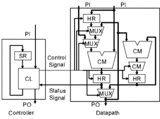
Figure 1: An RTL controller datapath circuit.
The rest of this paper is organized as follows. In Section 2, we define the target RTL circuits and the partially strong testability. We explain the overview of the proposed method in Section 3. The proposed DFT method and test generation method are introduced in Section 4 and 5, respectively. After discussing the experimental results in Section 6, Section 7 concludes this paper.
2. PRELIMINARIES
2.1 RTL Circuits
In RTL description, a circuit generally consists of a controller and a datapath. An example of an RTL circuit is shown in Figure 1. A controller consists of a state register (SR) and a combinational logic circuit (CL). A datapath consists of primary inputs (PI), pri- mary outputs (PO), hold registers (HR), load registers (LR), mul- tiplexers (MUX), combinational operational modules (CM). SRs, CLs, PIs, POs, HRs, LRs, MUXs and CMs are called hardware elements. Each hardware element has at most two data inputs, at most one control input, at most one status output and at most one data outputs. A SR has a data input and a data output. A CL has two data inputs, at most two data outputs, control outputs and status inputs.
Each hardware element is connected with signal lines. The signal lines are classified into data signal lines, control signal lines and status signal lines. A data signal line connects a data output to a data input. A control signal line connects a control output of a CL to a control input of a hardware element in a data path. A status signal line connects a status output of a hardware element in a datapath to a status input of a CL.
An RTL circuit is represented as an RTL graph whose vertices are inputs and outputs of hardware elements and whose edges are the signal lines and data flows between inputs and outputs of hard- ware elements. Let p= (e1,l1,e2, . . . ,ek−1,lk−1,ek) be a path start- ing from e1and ending at ek. eiand lidenote the vertex and the edge, respectively. The number of registers on p is called sequen- tial depth of p. p with no repeated vertices is called a simple path. pis called a loop if e1and ekare the same vertex and the path from e2to ek−1is a simple path. Different simple paths from eito ejare called re-convergent paths. If the sink vertex of a path p1 and the source vertex of a path p2 are identical, then we denote the con- catenation of the paths as(p1,p2). For each hardware element on p, the inputs and the outputs of the hardware element are called on- inputsand on-outputs respectively if they are on p. Similarly, the inputs and the outputs of the hardware element are called off-inputs and off-outputs respectively if they are not on p.
2.2 Strong Testability
In [10], a new testability for RTL datapaths called strong testa- bility was introduced as follows.
DEFINITION 1. (Strong Testability) A data path is said to be strongly testable if there exists a test plan for each hardware el- ement m that makes it possible to apply any pattern to m and to observe any response of m.
The strong testability is based on hierarchical test, and the test- ing is performed as follows: (1) test patterns are generated for each combinational hardware element m by using a combinational ATPG tool and (2) the test patterns are applied from PIs to m and the responses are observed at a PO by using the test plan for m. In order to guarantee the existence of the test plan for each hardware element, the DFT method proposed in [10] added thru function to every CM and hold function to some load registers. The thru func- tion of a CM provides a functionality to propagate values from its input to its output without any change. Test generation time for strongly testable datapaths is short since a combinational ATPG tool is used for each hardware element. However, it may not be necessary to have a test plan for every hardware element in order to achieve 100% FE. Moreover, since the DFT methods in [10] as- sumed that control/status signals from/to a controller are directly controllable/observable from the outside of circuits, Extra multi- plexers and an embedded test controller are required to provide the test plans when we consider whole RTL controller-datapath cir- cuits.
2.3 Partially Strong Testability
It is known that ATPGs for combinational circuits can achieve 100% FE in practical test generation time. For acyclic sequential circuits, it is also known that test patterns with 100% FE can be generated in practical test generation time on the time expansion model (TEM) [1]. Therefore, we expect that, for an RTL circuit, we can achieve 100% FE in practical test generation time if there exists a TEM such that the number of time frames required for any testable fault is bounded by a linear function of the number of reg- isters in it. In order to guarantee the existence of such TEM, only a part of hardware elements require the test plans. Therefore, we in- troduce such characteristic as partially strong testability. The par- tially strong testability is a characteristic for whole RTL controller- datapth circuits, and we don’t need explicit isolation for a controller and a datapath during DFT and test generation. Moreover, even if we focus on datapath part, a datapath with strong testability is a sub-class of a datapath with partially strong testability. Therefore, the hardware overhead of the proposed method can be expected to be lower than that of [10]. The formal definition of the partially strong testability is as follows.
DEFINITION 2. (Partially Strong Testability) An RTL circuit CD is said to be partially strongly testable if there exists a time expansion model such that the number of time frames is bounded by a linear function of the number of registers in CD and a test sequence can be generated on the time expansion model for any testable fault.
DEFINITION 3. (The Range of a Signal Line) A set of values that can appear at a signal line l in normal operation is said to be the range of l. The range of the input(output) of the hardware element connected with l is defined as the range of line l.
DEFINITION 4. (Dependency) Let Rliand Rl j be the range of signal lines liand lj, respectively. There exists a dependency be- tween liat time t and ljat time t′if licannot be set to any value in Rliat t when ljis set to any value in Rliat t′. A dependency be- tween input(output) connected with liand input(output) connected
with ljis defined as the dependency between liand lj.
DEFINITION 5. (Partially Strongly Testable Path) Let CD be an RTL circuit. A path pcis said to be a partially strongly testable path if pcsatisfies the following conditions for a loop c in CD.
1. Let pcinbe a simple path from a PI to an on-output of a hard- ware element mcinon c. Let pcoutbe a simple path from an on-output of a hardware element mcouton c to a PO. Let pc1 be c starting and ending at the on-output of mcin. Let pc2be a simple path from the on-output of mcinto the on-output of mcoutalong c. Then, pc= (pcin,pc1,pc2,pcout).
2. For any hardware element mion pcin, the on-output of mican be set to any value.
3. For any hardware element mion(pc1,pc2,pcout), there exists a value in the range of the off-input of misuch that the value can propagate any change at the on-input of mito the on- output of mi.
4. For any hardware element mion pc, let dibe the sequential depth of the path from the PI on pcto the on-input of mialong pc. There exists no dependency between the PI at time t and the on-input of miat time t+ di.
5. For any two hardware elements miand mjon pc, let diand djbe the sequential depth of the paths from the PI on pcto the on-input of miand mjalong pc, respectively. If di̸= dj,
there exists no dependency between each off-input of miat time t+ di and each off-input of mjat time t+ dj.
THEOREM 1. Let CD be an RTL circuit. Let dmaxbe the maxi- mum sequential depth of all partially strongly testable paths in CD. Let nREGbe the number of registers in CD. If there exists a par- tially strongly testable path pc for each loop c in CD, then there exists a time expansion model such that the number of times frames is at most dmax+ nREGand a test sequence can be generated on the time expansion model for any testable fault in CD.
From Definition 2 and Theorem 1, we have that any RTL cir- cuit which satisfies the condition of Theorem 1 is partially strongly testable.
3. OVERVIEW
First, we apply the DFT to make a given RTL circuit partially strongly testable. In the next section, the DFT problem we con- sider in this paper is formally presented and the DFT method is explained in detail. After that, we generate a TEM such that the number of time frames required for any testable fault is bounded by a linear function of the number of registers in the circuit. Then, a combinational ATPG is applied to the TEM. Test generation for the TEM requires a combinational ATPG which can deal with mul- tiple stuck-at faults. We use the circuit model which can express multiple stuck-at faults in a time expansion model as single stuck- at fault [11] in our experiments since TestGen (Synopsys) cannot deal with multiple stuck-at faults. Finally, we transform the test patterns for the TEM into test sequences for the RTL circuit.
The proposed DFT method consists of the following four steps: (1) construct a control forest, (2) construct a observation forest, (3) resolve dependencies and (4) generate a test controller. In Step 1, we decide a control path for each data input of each hardware element. The control path is used for propagating any value in the range of the data input. In order to guarantee the propagation through the control paths, we add thru functions if necessary. Sim- ilarly, in Step 2, we decide a observation path for each data output
PI
PO 0 1 TC
s1 m1 Controller
ADD1 PI
(a)Strong testability method [8]
CC TC
Controller
PI
PO 0 1 m1
ADD1 PI
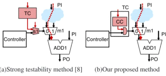
(b)Our proposed method Figure 2: Comparison of two methods.
of each hardware element. In Step 3, if there exists a dependency between inputs of a hardware element by using the paths decided in step 1 and 2, we resolve it by using hold functions of hold registers. We add hold function to load registers if necessary. In Step 4, a test controller is generated in order to activate the control/observation paths. Control signals for hold functions are also controlled by us- ing the test controller.
The proposed method tries to propagate values for control in- puts through the normal controller as much as possible while [8] always uses a test controller to provide the values. We can say the same thing for status inputs. Similarly, the proposed method tries to observe values from status/control outputs through the normal controller/datapath as much as possible while [8] always observe them directly by POs. Consequently, the complexity of the test controller and extra multiplexers can be reduced compared to [8]. This is because the partially strong testability does not require to control and observe any value for the signals between a datapath and a controller but requires to control and observe only any value in the range for them.
An example of the method proposed in [8] and an example of our proposed DFT method are shown in Figure 2(a) and 2(b), re- spectively. Suppose that MUX m1 exists on a control path (dotted line) for ADD1. In order to propagate values for ADD1 by using the path, the control signal of m1 should be ’0’. Both [8] and the proposed method provide the ’0’ from the test controller. Further- more, the control input of m1 must be able to be set to both ’0’ and
’1’ for testing m1 itself. In [8], these test patterns for the control input of m1 are also provided from the test controller. Therefore, test MUX s1 is added for switching the control signal from con- troller to the test controller(Figure 2(a)). On the other hand, in the proposed method, the test patterns for the control input of m1 are provided through the normal controller. Therefore, it is sufficient to provide ’0’ to the control input of m1 and only an AND gate is added in between the controller and the datapath (Figure 2(b)).
4. DFT METHOD
Before explaining the proposed method, we formally present a DFT problem for making a given RTL circuit partially strongly testable as follows.
DEFINITION 6. (DFT Problem for Partially Strong Testability) Given an RTL circuit CD, determine an augmented CD such that (1) the augmented CD is partially strongly testable and (2) the hardware overhead is minimized.
The proposed DFT method consists of the four steps explained in the previous section. The following subsections describe the details of the four steps.
4.1 Construct a Control Forest
We construct simple paths from PIs to data inputs of each hard- ware element. The simple path is called a control path and a set of
(a)A control forest. (b)An observation forest. Figure 3: Examples of forests.
the simple paths is called a control forest. A control path is guaran- teed to propagate any value in the range of each signal line. In order to propagate any value through the control paths, thru functions are added to hardware elements on the path if necessary. Then, we decide the control signals for the hardware elements on the path. From these control signals, a test controller is generated in Step 4. When we construct a control forest, we start searching control paths from a PI. Then, we decide a path from the PI to a hardware ele- ment. We try to minimize the number of additional thru functions by giving high priority to the hardware elements with thru functions for the path selection during the construction of the control forest.
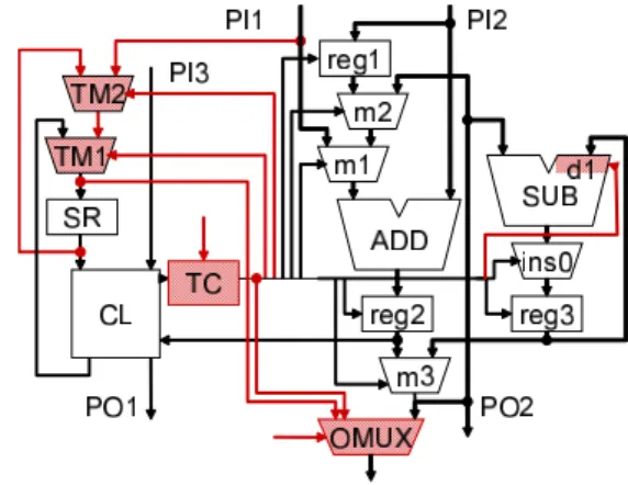
An example of the control forest for Figure 1 is shown in Figure 3(a). In this example, a thru function is added to SUB. An addi- tional path from PI1 to SR by the test multiplexer (TM1) is also added.
4.2 Construct an Observation Forest
We construct simple paths from the outputs of each hardware element to POs. The simple path is called an observation path and a set of the simple paths is called a observation forest. A observation path is guaranteed to propagate any value in the range of each signal line to a PO. In order to propagate any error by using observation paths, thru functions are added to hardware elements on the paths if necessary. Then, we decide the control signals for the hardware elements on the paths. From these control signals, a test controller is generated in Step 4. When we construct a observation forest, we start searching observation paths from a PO. Then, we decide a path from the PO to a hardware element. We try to minimize the number of additional thru functions and the required control signals by sharing the control paths and the observation paths as much as possible during the construction of the observation forest.
An example of the observation forest construction for Figure 1 is shown in Figure 3(b). Additional observation paths from CL to POs are added.
4.3 Resolve Dependencies
If there exist re-convergent paths in the control forest or the ob- servation forest and the sequential depth of the paths are the same, then there exists a dependency between the paths. If there exist dependencies, we decide registers which can resolve the dependen- cies and the number of the hold cycles to resolve them. The control signals to the registers for resolving the dependencies are provided from the test controller which is generated in Step 4. Moreover, the information of the hold cycles is used for the time expansion model generation shown in the next section. In the proposed method, we try to resolve the dependencies by using HRs as much as possible in order to reduce additional hold functions. In Figure 5, a hold function is added to SR by using test multiplexer TM2.
m1 m2 m3 ins0 reg1 reg2 reg3 d1 TM1 TM2
X X 1 X X X X X 1 1
0 0 0 0 1 1 1 1 1 0
0 0 0 0 0 1 1 1 1 0
T T T T 1 1 1 0 0 0
T T T T 1 1 1 0 1 0
T T T T T T T 0 0 X
T : output pattern of the CL X : don’t care
Figure 4: An example of output patterns of a test controller.
4.4 Generate a Test Controller
We generate a test controller(TC) which provides control signals for the control forest, the observation forest and resolving depen- dencies. TC is a combinational hardware element and the output patterns required for TC are selected by additional PIs. Let n be the number of output patterns of TC, then the number of additional PIs is⌈log2n⌉. TC is inserted between CL and the additional observa- tion paths added in Step 3. Moreover, the observation paths and the control signal lines for the additional hardware elements are also added from the TC.
An example of the test controller for the RTL circuit in Figure 1 is shown in Figure 4. 1st, 2nd and 3rd lines are the control signals for the control forest, the observation forest and resolving depen- dencies, respectively. 4th and 5th lines are the control signals for the testing of the RTL circuit. 6th line is the control signals for the normal operation. In this example, the number of additional PIs is 3 because the number of the output patterns of the TC is 6. More- over, by adding the TC, at most 2 gates which are an AND gate and an OR gate are inserted between the controller and the data path.
An example of partially strongly testable RTL circuit is shown in Figure 5. To reduce the pin overhead for additional observa- tion paths, a MUX (OMUX) is added to the PO in the datapaths to observe the additional observation paths. OMUX is controlled by additional PIs. By adding the OMUX, the pin overhead becomes the number of control inputs of the OMUX instead of the bit width of the additional observation paths.
Figure 5: An example of a partially strongly testable circuit.
5. TEST GENERATION METHOD
For the test generation of the partially strongly testable RTL cir- cuit, we generate a time expansion model (TEM) and a combina- tional ATPG is applied to the TEM. The TEM is generated as fol- lows. First, we generate a TEM that consists of a PO with time
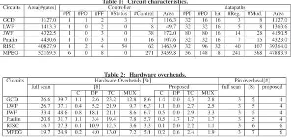
Table 1: Circuit characteristics.
Circuits Area[#gates] Controller datapaths
#PI #PO #FF #Status #Control Area #PI #PO bit #Reg. #Mod. Area
GCD 1127.0 1 1 2 3 7 116.3 32 16 16 3 8 1127.0
LWF 1413.3 1 0 2 0 8 49.7 32 32 16 5 8 1363.6
JWF 4322.5 1 0 3 0 38 172.0 80 80 16 14 28 4150.5
Paulin 4430.6 1 0 3 0 16 107.6 32 32 16 7 15 4323.0
RISC 40827.9 1 2 4 54 62 1463.9 32 96 32 40 107 39364.0
MPEG 52169.5 6 0 8 0 271 3459.8 56 148 8 241 368 47883.9
Table 2: Hardware overheads.
Circuits Hardware Overheads [%] Pin overhead[#]
full scan [8] Proposed full scan [8] proposed
C DP TC MUX C DP TC MUX
GCD 26.6 39.7 1.1 2.6 23.2 12.8 8.6 1.4 0.0 4.3 2.8 3 5 4
LWF 26.7 37.1 0.4 5.2 21.9 9.7 6.3 1.1 0.0 2.7 2.5 3 5 4
JWF 33.4 48.6 0.8 18.1 21.1 8.6 6.7 0.5 0.0 2.9 3.3 3 5 4
Paulin 20.8 31.7 1.1 3.4 19.4 7.8 5.7 0.5 1.7 1.7 1.7 3 5 4
RISC 16.7 27.3 0.1 10.9 12.5 3.6 3.3 0.1 0.0 2.2 1.1 3 6 6
MPEG 19.7 24.9 0.2 4.0 13.0 7.2 5.1 0.2 0.6 2.4 1.9 3 7 6
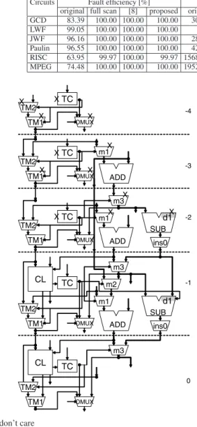
frame 0. Then, a hardware element m connected to the PO and the signal line between m and the PO are added to the TEM. When m is added to the TEM for the first time, all the hardware elements connected with inputs of m are added to the TEM. When m which already exists in the TEM is added to the TEM again, only the hardware elements connected on the control forest are added to the TEM. Moreover, all the hardware elements which exists on the ob- servation path for m and the corresponding signal lines are also added to the TEM. If m is a register, then only the signal line con- nected with m is added to the TEM and the time frame is decreased by 1. If m is used to resolve the dependencies, the time frame is decreased by the corresponding hold cycles. This process repeats until m becomes a PI and all POs are added to the TEM. An exam- ple of the TEM for Figure 5 is shown in Figure 6.
A combinational ATPG is applied to the generated TEM. Then, generated test patterns are transformed so that the test patterns can be applied to the original RTL circuit.
6. EXPERIMENTAL RESULTS
We evaluated the effectiveness of the proposed method by ex- periments. RTL benchmark circuits used for the experiments are GCD, LWF, JWF and PAULIN which are popularly used circuits, and RISC and MPEG which are more practical and larger circuits designed by a semiconductor company. Characteristics of these cir- cuits are shown in Table 1. “#PI” and “#PO” denote the numbers of primary inputs and outputs, respectively. “#FF”, “#state” and
“#Control” denote the numbers of FFs, status inputs and control outputs, respectively. “#Reg” and “#Mod.” denote the numbers of registers and the number of hardware elements except for regis- ters, respectively. “bit” denotes the bit width of the datapaths. In our experiments, we used AutoLogicII (MentorGraphics) as a logic synthesis tool with its sample libraries to synthesize those circuits. In Table 1, “Area” denotes the total circuit size. We compared the proposed method with original circuits, the full-scan method and the method of [8]. In the full scan method, all FFs in the circuits are replaced by the scan-FFs and single scan chain is constructed.
The results of the hardware overhead are shown in Table 2. “C”,
“DP”, “TC” and “MUX” denote the hardware overhead of con- troller, datapath, test controller and additional MUXs, respectively. The hardware overhead of the proposed method is much smaller than others. Compared to [8], we can see that the reduction of the hardware overhead mainly comes from the test controller and
the additional MUXs. Moreover, delay overhead of the proposed method is lower than that of [8]. This is because at most 2 gates are inserted in between controller and datapath in the proposed method while at most 4 gates are inserted in between them in [8]. We can also observe that pin overhead is smaller than [8]. In the proposed method, the pin overhead of RISC and MPEG is larger than other benchmark circuits. This is because the number of control signals utilizing for hold functions is large for RISC. Moreover, in RISC and MPEG, 2 or more OMUX were required because the bit-width of the control outputs of the TC was larger than the bit-width of POs in the datapath part.
The test generation results are shown in Table 3. We used Test- Gen (Synopsys) as a sequential and combinational ATPG tool on Sun Blade 2000 (Sun Microsystems). Test generation for sequen- tial circuits using TEM requires a combinational ATPG which can deal with multiple stuck-at faults. In this experiments, since Test- Gen cannot deal with multiple stuck-at fault, we use the circuit model which can express multiple stuck-at faults in a time expan- sion model as single stuck-at fault [11]. “Test generation time” de- notes the time spent for ATPG and does not include the time spent for the proposed DFT because it is negligible compared to the time for ATPG. We observe that the full-scan method, the method of [8] and the proposed method can achieve 100% FE except RISC in practical test generation time. For RISC, the full-scan method and the proposed method cannot generate test vectors for some faults in the datapath. For MPEG, test generation time of the proposed method is longer compared to the full-scan method. This is be- cause the sequential depth of a simple path from PI to PO is long and the scale of the time expansion model became large.
In the results of test application time, the proposed method can achieve up to 99.6% reduction compared to the full-scan method. This is because the proposed method does not require scan-shift operations. The proposed method can also allow at-speed testing because the test pattern can be applied only by the system clock. In comparison with the method in [8], the proposed method can also obtain savings in test application time up to 94.3%. We con- sider that faults were efficiently detected by the fault simulation in the proposed method since the whole circuit is the target for test generation while [8] is based on hierarchical test generation and a ATPG is applied to each module separately. The proposed method requires longer test generation time compared to the previous meth- ods. However, the test application time is per chip cost while the
Table 3: Test generation results.
Circuits Fault efficiency [%] Test generation time[sec] Test application time [clock] original full scan [8] proposed original full scan [8] proposed original full scan [8] proposed
GCD 83.39 100.00 100.00 100.00 3070.07 0.27 1.13 1.72 421 4232 456 588
LWF 99.05 100.00 100.00 100.00 85.45 0.17 0.89 1.01 392 2904 295 108
JWF 96.16 100.00 100.00 100.00 2873.34 0.88 1.22 5.91 412 20975 1000 675
Paulin 96.55 100.00 100.00 100.00 4290.51 0.53 1.60 8.07 201 6147 1136 798
RISC 63.95 99.97 100.00 99.97 156808.67 98870.71 105.26 166.88 6928 1233859 7914 4345 MPEG 74.48 100.00 100.00 100.00 195260.82 55.72 17.64 1208.90 148 462942 150019 8515
m1 CL TC m2
TM1 OMUX m3
d1
-1 -2 -3 -4
SUB ADD ins0
TM2
CL TC
TM1 OMUX m3
TM2
TC m1 TM1 OMUX
m3
d1 SUB ADD ins0
TM2
TC m1
TM1 OMUX ADD
TM2
TM1 OMUX
TM2 TC
X X
X X
X X
X
X X X
X X
0
X: don’t care
Figure 6: An example of the time expansion model.
test generation time is one time cost for a design. Therefore, the proposed method can reduce the total test cost effectively.
7. CONCLUSION
In this paper, we defined the partially strong testability as a char- acteristic of RTL controller-datapath circuits. We also proposed a DFT method and a test generation method based on the partially strong testability. The proposed method can achieve 100% FE in practical test generation time by using a combinational ATPG. It also allows at-speed testing. Furthermore, the proposed method can reduce hardware overhead and test application time drastically compared to [8] by paying an acceptable cost for test generation time. Test application time and hardware overhead cost every man- ufactured chip while test generation time is one time cost for a design before manufacturing. Therefore, the proposed method is effective.
8. ACKNOWLEDGMENTS
The authors would like to thank Prof. M. Inoue and Dr. S. Ohtake of Nara Institute of Science and Technology for their valuable dis- cussions. This work was supported in part by 21st Century COE Program and in part by Japan Society for the Promotion of Sci- ence (JSPS) under Grants-in-Aid for Scientific Research B(2)(No. 15300018).
9. REFERENCES
[1] T. Inoue, D. K. Das, T. Mihara, C. Sano, and H. Fujiwara,
“Test generation for acyclic sequential circuits with hold registers,” in Proc. Int. Conf. on Computer-Aided Design, pp. 550–556, Nov. 2000.
[2] S. Dey and M. Potkonjak, “Non-scan design-for-testability of RT-level data paths,” in Proc. Int. Conf. on Computer-Aided Design, pp. 640–645, Nov. 1994.
[3] R. B. Norwood and E. J. McCluskey, “Orthogonal scan:Low overhead scan for data paths,” in Proc. Int. Test Conf., pp. 659–668, Oct. 1996.
[4] R. B. Norwood and E. J. McCluskey, “High-level synthesis for orthogonal scan,” in Proc. VLSI Test Symp., pp. 370–375, Apr. 1997.
[5] J. Lee and J. Patel, “Hierarchical test generation under architectural level functional constraints,” IEEE Trans. Computer-Aided Design, vol. 15, pp. 1144–1151, Sep. 1996. [6] I. Ghosh, A. Raghunathan, and N. K. Jha, “Design for
hierarchical testability of RTL circuits obtained by behavioral synthesis,” in Proc. Int. Conf. on Computer Design, pp. 173–179, Oct. 1995.
[7] I. Ghosh, A. Raghunathan, and N. K. Jha, “A
design-for-testability technique for register-transfer level circuits using control/data flow extraction,” IEEE Trans. Computer-Aided Design, vol. 17, pp. 706–723, Aug. 1998. [8] S. Ohtake, H. Wada, T. Masuzawa, and H. Fujiwara, “A
non-scan DFT method at register-transfer level to achieve complete fault efficiency,” in Proc. Asia and South Pacific Design Automation Conf., pp. 599–604, Jan. 2000.
[9] S. Ohtake, T. Masuzawa, and H. Fujiwara, “A non-scan DFT method for controllers to achieve complete fault efficiency,” in Proc. Asian Test Symp., pp. 204–211, Dec. 1998. [10] H. Wada, T. Masuzawa, K. K. Saluja, and H. Fujiwara,
“Design for strong testability of RTL data paths to provide complete fault efficiency,” in Proc. Int. Conf.on VLSI Design, pp. 300–305, Jan. 2000.
[11] H. Ichihara and T. Inoue, “A method of test generation for acyclic sequential circuits using single stuck-at fault combinational ATPG,” IEICE Trans. Fundamentals, vol. E86-A, pp. 3072–3078, Dec. 2003.