Design for Consecutive Transparency of Cores in System-on-a-Chip
Tomokazu Yoneda and Hideo Fujiwara
Graduate School of Information Science, Nara Institute of Science and Technology
8916-5 Takayama, Ikoma, Nara, 630-0101, Japan
Tel : +81-743-72-5223 Fax : +81-743-72-5229
yoneda, fujiwara @is.aist-nara.ac.jp
Abstract
This paper presents a design-for-consecutive- transparency method that makes a soft core (RTL description) consecutively transparent using integer linear programming. Consecutive transparency of a core guar- antees consecutive propagation of arbitrary test/response sequences from the core inputs to the core outputs with some latency. Therefore, it is possible to apply/observe arbitrary test/response sequences to/from an embedded core consecutively at the speed of system clock by using interconnects and consecutively transparent cores in an SoC. Experimental results show that the proposed method introduces lower area overhead compared to the bypass method that adds direct paths from PIs to POs with multiplexers.
keywords: design for testability, systems-on-a-chip, test access mechanism, consecutive transparency, consecutive testability, register transfer level
1 Introduction
A fundamental change has taken place in the way digital systems are designed by making it possible to design an entire system, containing hundred millions of transistors, on a single chip. In order to cope with the growing complexity of such systems, designers often use pre-designed, reusable megacells known as cores. Core-based systems-on-a-chip (SoC) design strategies help companies significantly reduce the time-to-market and design cost for their new products.
However, it is difficult to test SoCs after fabrication[1]. A major problem to make an SoC testable concerns acces- sibility of embedded cores. Several design-for-testability (DFT) techniques have been proposed. There are three main approaches to achieve accessibility of embedded cores. The first approach is based on test bus architectures by which the cores are isolated from each other in test mode using a dedicated bus [4, 5, 6, 7, 8] or flexible TESTRAIL [9] around the cores to propagate test data. The second approach uses boundary scan architectures[2, 3] to isolate the core during test. The third approach uses transparency [11, 12, 13, 10] for embedded cores to reduce the problem to one of finding paths from PIs to core inputs and from core outputs to POs. Under the design environment for SoCs, pre-computed test sets are provided for each core. These test sets may
contain functional vectors, scan vectors or ordered test se- quences for non-scan designed sequential circuits. They may be for logic faults such as stuck-at faults or timing faults such as delay faults. Moreover, some cores may be able to be at-speed testable in order to increase the coverage of non-modeled and performance-related defects. For that reason, it is necessary to apply an arbitrary test sequence to each core and observe its response sequence from the core consecutively at the speed of the system clock. We call such a test access consecutive test access.
There are two works [14, 15] realizing the consecutive test access for both cores and interconnects. In [14], we proposed a kind of testability of SoCs called consecutive testabilityand consecutively transparency of cores. Consec- utive transparency of a core guarantees consecutive propa- gation of arbitrary test/response sequences from the core in- puts to the core outputs with some latency. Therefore, con- secutively testability of SoCs guarantees that it is possible to apply/observe arbitrary test/response sequences to/from an embedded core consecutively at the speed of system clock by using interconnects and consecutively transparent cores. In [15], a synthesis-for-transparency approach was presented to make cores single-cycle transparent by em- bedding multiplexers. This single-cycle transparency is a special case of consecutive transparency of [14] such that the latency of the consecutive transparency is restricted to zero, i.e., single-cycle transparency is the consecutive trans- parency with zero latency. However, the area overhead for making cores single-cycle transparent (i.e., transparent with zero latency) is generally higher than that for making cores consecutively transparent with some latency.
Cores are classified into three types: soft (RTL descrip- tion), firm (netlist) or hard (layout). In [14], we assumed that the internal design of all cores cannot be modified by DFT due to IP (Intellectual Property) protection and when a core in a given SoC is not consecutively testable, direct paths from PIs to the core (from the core to POs) are added by inserting test multilexers in the proposed DFT. In this way, we can bypass a core with multiplexers independently of internal structure of the core. However, when a core is delivered as soft core, we can modify internal design of the core. In this paper, we propose a design-for-consecutive- transparency (DFCT) method that makes a soft core consec- utively transparent using integer linear programming (ILP).
21st IEEE VLSI Test Symposium (VTS'03), pp.287-292, April-May 2003.
The DFCT method realizes consecutive transparency by uti- lizing paths that exist in data path part of an RTL circuit. Experimental results show that the proposed method intro- duces lower area overhead compared to the above men- tioned bypass method. Therefore, by preparing a consec- utively transparent version of each soft core in addition to original core, we can expect that the proposed DFT method in [14] introduces lower area overhead for making a given SoC consecutively testable.
The rest of this paper is organized as follows. Sec- tion 2 gives the definitions of consecutive transparency and RTL circuits. In section 3, we introduce the design-for- consecutive-transparency method. Experimental results are discussed in section 4. Finally, section 7 concludes this pa- per.
2 Preliminaries
2.1 Consecutive Transparency of a Core
Definition 1 Consecutive transparency of a core
Let I i be the ith bit of a PI I, and O j be the jth bit of a PO O. Suppose that there exists a configuration (test mode) of a core which can realize a path P between I i and O j . P is called a consecutively transparent path if any in- put sequence applied to I i can be consecutively observed at O j after some latency, and then I i and O j are said to be consecutively transparent. Moreover, a core is called to be consecutively transparent if, for each PI/PO of the core, there exists a configuration that can make all bits of the port consecutively transparent.
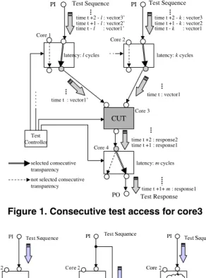
2.2 Consecutive Testability of a System-on-a-Chip In [14], we proposed a new test methodology based on consecutive testability of SoCs and consecutive trans- parency of cores. Figure 1 illustrates a consecutively testable SoC and the consecutive test access to/from Core 3. A control signal is provided for each consecutively trans- parent core by a test controller (either off-chip or on-chip). Each of the control signal determines the current test mode of the core called a configuration. In Figure 1, a configura- tion of each core is determined and consecutively transpar- ent paths for shaded ports are realized. Consecutive testa- bility of an SoC guarantees that, for each core (for each in- terconnect) in the SoC, by selecting configurations of other cores, arbitrary test sequence can be consecutively fed into the core (the interconnect, respectively) from PIs and its re- sponse sequence can be consecutively propagated to POs through consecutively transparent paths in other cores and interconnects.
In [14], we assumed that the internal design of all cores cannot be modified by DFT due to IP protection and when a core in a given SoC is not consecutively testable (Fig- ure 2(a)), direct paths from PIs to the core (from the core
CUT
Test Sequence
time t : vector1 time t : vector1’
Test Sequence
time t +2 : response2 time t +1 : response1
time t +1+ m : response1 PO
PI PI
Test Controller
selected consecutive transparency not selected consecutive transparency
latency: l cycles latency: k cycles
latency: m cycles time t +2 - k : vector3 time t +1 - k : vector2 time t - k : vector1 time t +2 - l : vector3’
time t +1 - l : vector2’ time t - l : vector1’
Test Response Core 1
Core 2
Core 3
Core 4
Figure 1. Consecutive test access for core3
Figure 2. DFT for consecutive test access to POs) are added by inserting test multilexers in the pro- posed DFT (Figure 2(b)). However, when a core is de- livered as soft core, we can modify internal design of the core. In this paper, we propose a design-for-consecutive- transparency (DFCT) method that makes a soft core con- secutively transparent by utilizing paths that exist in data path part of an RTL circuit (Figure 2(c)). Experimental re- sults show that the proposed method introduces lower area overhead compared to the above mentioned bypass method. Therefore, by preparing a consecutively transparent version of each soft core in addition to original core, we can expect that the proposed DFT method in [14] introduces lower area overhead for making a given SoC consecutively testable. 2.3 RTL Circuits
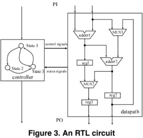
In RTL description, a circuit generally consists of a con- troller and a data path as shown in Figure 3. The former is represented by a finite state machine (FSM) and the latter is represented by hardware elements (e.g. registers, multi- plexers (MUXes) and operational modules) and signal lines connecting them. Each of the controller and the data path has primary inputs from the outside of the circuit and pri-
Figure 3. An RTL circuit
mary outputsto the outside of the circuit. The controller also has status inputs from the data path and control outputs to the data path. Similarly, the data path also has control in- putsfrom the controller and status outputs to the controller. The signals from the controller to the data path are called control signals, and the signals from the data path to the controller are called status signals.
A data path consists of hardware elements and signal lines. Hardware elements are primary inputs (PIs), pri- mary outputs (POs), control inputs, status outputs, regis- ters, MUXes and operational modules. We introduce ports of each hardware element as interface points in a natural fashion: signals enter into a hardware element through its input ports, and exit through its output ports. Input ports of a hardware element can be classified into data input ports and control input ports. Similarly, output ports of a hard- ware element can be classified into data output ports and status output ports. A signal line connects two ports with some bit width. Any number of signal lines can connect to the same output port (i.e. fanout is allowed), but only one signal line can connect to the same input port. In order to simplify the discussion, the following restrictions are intro- duced into data path architecture. (1)All signal lines have the same bit width. (2)Control input ports of a hardware element are connected directly to control inputs of the data path. And status output ports of a hardware element are connected directly to status outputs of the data path. 2.4 Port Graph
Definition 2 Port Graph
We define a port graph G V E as a directed graph to represent an RTL circuit.
V VPI VPO Vport where
VPI is the set of all PIs in the RTL circuit, VPOis the set of all POs in the RTL circuit, Vport is the set of all ports in the RTL circuit.
E x y V V
Figure 4 illustrates a port graph corresponding to an RTL circuit as shown in Figure 3.
Figure 4. A port graph
3 Design for Consecutive Transparency
In this section, we present a design-for-consecutive- transparency (DFCT) method that makes an RTL circuit consecutively transparent using integer linear program- ming.
3.1 Problem Formulation
A consecutively transparent circuit has consecutively transparent paths for each PIs and POs. When a given RLT circuit does not have such paths for each PIs(POs), DFCT elements are added in order to make the circuit consecu- tively transparent as follows.
Case I : There exits a path from the PI(PO) to a PO(PI) through a MUX or register, and normal operational mode (control signals from controller) can not propa- gate an arbitrary sequence through the path due to hold behavior of the register or switching behavior of MUX. DFCT elements: AND gate, OR gate and MUX
In order to propagate an arbitrary sequence through the path, we fix the control signal (from controller to the MUX or register) on the desired value by DFCT ele- ments as follows (Figure 5).
In case 0-controllability is necessary on the con- trol signal, an AND gate is added to the control signal.
In case 1-controllability is necessary on the con- trol signal, an OR gate is added to the control signal.
In case general-controllability is necessary on the control signal, an MUX is added to the control signal.
Case II : There exits a path from the PI(PO) to a PO(PI) through an operational module, and the path can not propagate an arbitrary sequence.
DFCT element: thru function
In order to propagate an arbitrary sequence through the path, we augment the module with thru function if nec- essary (Figure 6).
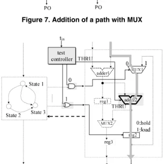
Case III : There exits no path from the PI(PO) to a PO(PI).
Figure 5. Fix control signal on desired value
Figure 6. Thru function
DFCT element: MUX
In order to propagate an arbitrary sequence from the PI(PO) to a PO(PI), we add a direct path from the PI(PO) to a PO(PI) with MUX (Figure 7).
Added DFCT elements are controlled by signals from a test controller. Figure 8 shows a test architecture of the pro- posed method. In this figure, 0-controllability of MUX1, thru function of adder2 and 1-controllability of reg2 are added, and a consecutively transparent path (shaded line) is realized by the control signal from the test controller.
m
Definition 3 The design for consecutive transparency (DFCT) is formulated as the following optimization prob- lem.
Input: An RTL circuit ( a port graph)
Output: A consecutively transparent RTL circuit
Optimization: Minimizing hardware overhead (i.e., hard- ware of added DFCT elements)
3.2 DFCT Algorithm
In this subsection, we propose a DFCT algorithm. The algorithm consists of the following two steps.
Step 1 For a given port graph (an RTL circuit), add edges which can be realized by DFCT elements.
Step 2 For each PI and PO, induce constraints such that the PI (PO) has a consecutively transparent path, and for- mulate DFCT as an ILP problem to minimize hardware overhead.
Step 1: Addition of edges to a port graph
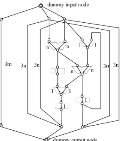
For a port graph, the algorithm adds edges and vertices as follows (Figure 9).
a dummy input vertex and edges from the dummy in- put vertex to all v VPI
a dummy output vertex and edges from all v VPOto the dummy input vertex
edges from data input ports of a MUX to a
Figure 7. Addition of a path with MUX
Figure 8. Test architecture of the proposed method data output port of the MUX (These edges are realized by AND gates for 0-controllability, OR gates for 1-controllability, and MUXes for general- controllability.)
edges from data input ports of a operational module to a data output port of the operational module (These edges are realized by thru functions.)
edges from a data input port of a register to a data output port of the register (These edges are realized by AND gates for 0-controllability, OR gates for 1-controllability, and MUXes for general- controllability.)
edges from each PI to all PO in data path (These edges are realized by MUXes.)
edges from each PI to all PO in controller (These edges are realized by MUXes.)
Then, the algorithm defines cost of each edge as the hard- ware cost that is necessary to realize the edge by DFCT el- ements (i.e. AND gate, OR gate, thru function and MUX), and defines capacity of each edge as 1. Figure 9 shows , examples of the hardware costs when all signal lines in the data path have n bit width.
Step 2: An ILP formulation for DFCT
For the port graph extended in Step 1, DFCT is formu- lated as an ILP problem represented by equations (1) to (8) with the following 0-1 variables.
xv e
1 Edge e Eis used as a part of consecutively transparent path for port v VPI VPO. 0 otherwise
Figure 9. Addition of edges and cost to a port graph
xe
1 Edge e Eis used as a part of consecutively transparent path for more than one port v VPI VPO. 0 otherwise
Minimize:
∑
e E
xe cost e (1)
cost e is a constant value which represents the hardware cost to realize edge e with a DFCT element.
Subject to:
1. For each PI vpi VPI,
1
∑
e Evpiout
xvpie (2)
∑
e Evdoin
xvpie 1 (3)
∑
e Evin
xvpie
∑
e Evoutxvpie
for all v V vpi vdo
(4) vdi and vdo denote dummy input vertex and dummy output vertex, respectively. Evin and Evout denote the set of all input edges and the set of all output edges, respectively.
2. For each PO vpo VPO,
1
∑
e Evdiout
xvpoe (5)
∑
e Evpoin
xvpoe 1 (6)
∑
e Evin
xvpoe
∑
e Evoutxvpoe
for all v V vdi vpo
(7) 3. For each edge e E,
xe xv e for all v V (8)
Equations (2), (3) and (4) are constraints such that the port graph has flow of value 1 from PI vpito dummy output ver- tex vdo. For each vertex, these equations guarantee that the sum of input flows is equal to the sum of output flow. Simi-
Table 1. Characteristics of RTL Benchmark Circuits
larly, equations (5), (6) and (7) are constraints such that the port graph has flow of value 1 from dummy input vertex vdi
to PO vpo. Equations (1) and (8) minimize hardware over- head. We can find consecutively transparent paths for all PIs and POs with minimum hardware overhead by the solv- ing above ILP problem, and DFCT elements are added to realize those paths.
In this paper, we showed the method to minimize hard- ware overhead only. However, we can avoid delay overhead by making costs of the edges in critical paths of a circuit high.
4 Experimental Results
In this section, we present experimental results obtained by the proposed method. Circuit characteristics of RTL benchmark circuits used in the experiments are shown in Table 1. These circuits are examples used popularly. In our experiments, we used Design Compiler (Synopsys) to synthesize those benchmark circuits. In this table, columns
“#PI” and “#PO” of columns “Controller” and “Datapath” denote the number of PIs and POs of respective parts. Col- umn “ bit ” denotes the bit width of data paths. Column
“Area” denotes the total area after synthesis. Here, areas are estimated using gate equivalent of library cell area.
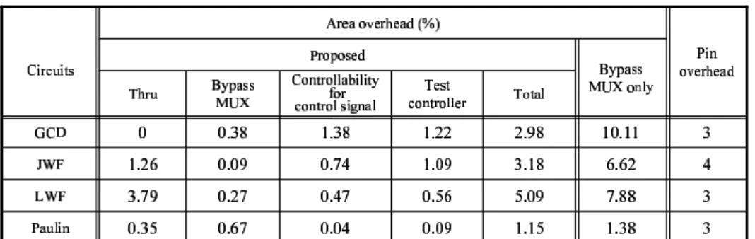
The area and pin overhead of the proposed method are shown in Table 2. We used the lp solve package from Eind- hoven University of Technology [16]. The running time is negligible (less than 0.1 second) for all four benchmark cir- cuits on a SUN Ultra 5 workstation. Columns “Thru”, “By- pass MUX”, “Controllability for control signal” and “Test controller” in column “Proposed” of column “Area over- head” denote the area overhead of the proposed method added by thru functions, bypass MUXes, primitive gates on control signal and test controller, respectively. Column
“Bypass MUX only” of column “Area overhead” denotes the area overhead of the bypass method that adds direct paths from PIs to POs with MUXes.
From the experimental results, we can see that the pro- posed method introduces lower area overhead compared to the bypass method in all circuits. In the proposed method, we can guarantee that a consecuitvely transparent path for each PI/PO can be realized by adding at most one MUX since we consider utilization of existing paths in data path as well as addition of bypass routes with MUXes. Column
“Pin overhead” in Table 2 denotes the number of additional
Table 2. Hardware Overhead
pins for consecutive transparency. In proposed method, we need log2n 1 additional pins. Here, n is a total number of PIs and POs of a circuit. These additional pins are used for identifying modes of the circuit (i.e. normal mode and consecutively transparent modes (configurations)). Since circuits are embedded into an SoC as cores, those additional pins of the circuits for consecutive transparency do not re- sult in pin overhead of the SoC directly.
5 Conclusions
In this paper, we proposed a design-for-consecutive- transparency method that makes a soft core consecu- tively transparent using ILP. Consecutive transparency of a core guarantees consecutive propagation of arbitrary test/response sequences from the core inputs to the core outputs with some latency. Therefore, it is possible to apply/observe arbitrary test/response sequences to/from an embedded core consecutively at the speed of system clock by using interconnects and consecutively transparent cores in an SoC. The DFCT method realizes consecutive trans- parency with low area overhead (average 3.1%) by utilizing paths that exist in data path of an RTL circuit. Experimental results show that the proposed method introduces lower area overhead compared to the bypass method. Therefore, by preparing a consecutively transparent version of each soft core in addition to original core, we can expect that the pro- posed DFT method in [14] introduces lower area overhead for making a given SoC consecutively testable.
Acknowledgments
This work was sponsored in part by NEDO (New En- ergy and Industrial Technology Development Organization) through the contract with STARC (Semiconductor Technol- ogy Academic Research Center) and supported in part by Foundation of Nara Institute of Science and Technology un- der the Grant for Activity of Education and Research. Au- thors would like to thank Dr. Michiko Inoue, Dr. Satoshi Ohtake and Dr. Erik Larsson (Nara Institute of Science and Technology) for their valuable discussion.
References
[1] Y.Zorian, E.J.Marinissen and S.Dey, “Testing embedded-core based system chips,” Proc. 1998 Int. Test Conf., pp.130-143, Oct. 1998. [2] N.A.Touba and B.Pouya, “Testing embedded cores using partial iso-
lation rings,” Proc. 15th VLSI Test Symp., pp.10-16, May 1997. [3] L.Whetsel, “An IEEE 1149.1 based test access architecture for ICs
with embedded cores, ” Proc. 1997 Int. Test Conf., pp.69-78, Nov. 1997.
[4] S.Bhatia, T.Gheewala and P.Varma, “A unifying methodology for in- tellectual property and custom logic testing,” Proc. 1996 Int. Test Conf., pp.639-648, Oct. 1996.
[5] T.Ono, K.Wakui, H.Hikima, Y.Nakamura and M.Yoshida, “Inte- grated and automated design-for-testability implementation for cell- based ICs,” Proc. 6th Asian Test Symp., pp.122-125, Nov. 1997. [6] P.Varma and S.Bhatia, “A structured test re-use methodology for
core-based system chips,” Proc. 1996 Int. Test Conf., pp.294-302, Oct. 1998.
[7] K.Chakrabarty, “Design of System-on-a-Chip Test Access Archi- tectures Using Integer Linear Programming,” Proc. 18th VLSI Test Symp., pp.127-134, May 2000.
[8] K.Chakrabarty, “Design of System-on-a-Chip Test Access Architec- tures under Place-and-Route and Power Constraints,” Proc. 37th De- sign Automation Conf., pp.432-437, June 2000.
[9] E.Marinissen, R.Arendsen, G.Bos, H.Dingemanse, M.Lousberg and C.Wouters, “A Structured and Scalable Mechanism for Test Access to Embedded Reusable Cores,” Proc. 1998 Int. Test Conf., pp.284- 293, Nov. 1998.
[10] M.Nourani and C.A.Papachristou, “Structural fault testing of em- bedded cores using pipelining,” Journal of Electronic Testing:Theory and Applications 15, pp.129-144 1999.
[11] I.Ghosh, N.K.Jha and S.Dey, “A low overhead design for testabil- ity and test generation technique for core-based systems-on-a-chip,” IEEE Trans. on CAD, vol.18, no.11, pp.1661-1676, Nov. 1999. [12] I.Ghosh, S.Dey, and N.K.Jha, “ A fast and low cost testing technique
for core-based system-chips,” IEEE Trans. on CAD, vol.19, no.8, pp.863-877, Aug. 2000.
[13] S.Ravi, G.Lakshminarayana, and N.K.Jha, “ Testing of Core-Based Systems-on-a-Chip,” IEEE Trans. on CAD, vol.20, no.3, pp.426-439, Mar. 2001.
[14] Tomokazu Yoneda and Hideo Fujiwara, ”Design for Consecutive Testability of System-on-a-Chip with Built-In Self Testable Cores,” Journal of Electronic Testing: Theory and Applications (JETTA) Special Issue on Plug-and-Play Test Automation for System-on-a- Chip, Vol. 18, No. 4/5, pp.487-501, Aug./Oct. 2002.
[15] K.Chakrabarty, R.Mukherjee and A.Exnicios, “Synthesis of Trans- parent Circuits for Hierarchical and System-on-a-Chip Test,” Proc. IEEE International Conference on VLSI Design, pp.431-436, Jan. 2001.
[16] M.Berkelaar, lp solve, version 3.2, Eindhoven University of Tech- nology, The Netherlans, ftp://ftp.ics.ele.tue.nl/pub/lp solve.