Power-Constrained Test Scheduling for Multi-Clock Domain SoCs
Tomokazu Yoneda†, Kimihiko Masuda‡ and Hideo Fujiwara†
†Graduate School of Information Science, Nara Institute of Science and Technology
Kansai Science City, 630-0192, Japan
{yoneda, fujiwara}@is.naist.jp
‡SHARP CORPORATION
Abstract
This paper presents a wrapper and test access mecha- nism design for multi-clock domain SoCs that consists of cores with different clock frequencies during test. We also propose a test scheduling algorithm for multi-clock domain SoCs to minimize test time under power constraint. In the proposed method, we use virtual TAM to solve the frequency gaps between cores and the ATE, and also to reduce power consumption of a core during test while maintaining the test time of the core. Experimental results show the effectiveness of our method not only for multi-clock domain SoCs, but also for single-clock domain SoCs with power constraints. keywords: multi-clock domain SoC, test scheduling, test access mechanism, power consumption
1 Introduction
The systems-on-chip (SoC) design strategies help us to reduce the time-to-market and design cost for new prod- ucts significantly. However, testing of SoC is a crucial and time consuming problem due to the increasing de- sign complexity[1]. Therefore, the goal is to develop tech- niques for wrapper design, test access mechanism (TAM) design and test schedule that minimizes test application time under given constraints such as the number of test pins and power consumption. A number of approaches have addressed wrapper design [2, 3, 4] which are IEEE 1500 [5] compliant. Similarly, several TAM architectures have been proposed such as TestBus [6, 7], TESTRAIL [8], transparency based TAM[9, 10, 11]. Moreover, many ap- proaches for test scheduling problem have been proposed [12, 13, 14, 15, 16, 17].
However, these previous approaches are applicable only to single-clock domain SoCs that consist of embedded cores working at the same clock frequency during test. Today’s SoC designs in telecommunications, networking and digital signal processing applications consist of embedded cores working with different clock frequencies. The clock fre- quency of some embedded cores during test is limited by its scan chain frequencies. On the other hand, other cores may be testable at-speed in order to increase the coverage of non-modeled and performance-related defects. The at- speed testable cores might be non-scan designed sequential circuits and require functional vectors or ordered test se- quence at the rated clock frequency. Moreover, there also
exists a frequency gap between each embedded core and ATE used to test the SoC. From these facts, we conclude that the previous approaches have the following two prob- lems: 1) in the case when test clock frequency of a core is higher than that of ATE, the ATE cannot provide test se- quences at the same speed of the test clock frequency of the core, and 2) in the case when test clock frequency of a core is lower than that of ATE, testing of the core by lowering the frequency of ATE does not make use of ATE capability ef- fectively. Therefore, it is necessary to develop a technique that can solve the above problems for the multi-clock do- main SoCs.
Recently, virtual TAM based on bandwidth matching [18] has been proposed in [19] to increase ATE capability when the clock frequency of a core is lower than that of ATE. Xu et al. extended the virtual TAM technique to the multi-frequency TAM design to reduce the test time for the single-clock domain SoCs in [22]. Moreover, a wrapper de- sign for cores with multiple clock domains was proposed in [20, 21] to achieve at-speed testing of the cores by using vir- tual TAM technique. However, the test scheduling problem for the multi clock domain SoCs is not addressed in these literatures.
To the best of our knowledge, this paper gives a first dis- cussion and a formulation of the test scheduling problem for multi-clock domain SoCs. We present a wrapper and TAM design for multi-clock domain SoCs and propose a test scheduling algorithm to minimize test time under power constraint. In the proposed method, we use virtual TAM for each core to solve a frequency gap between each core and a given ATE while the approach in [22] uses a virtual TAM for each test bus (i.e., all the cores assigned to the same test bus must be tested at the same frequency). Therefore, the proposed method in this paper has more flexibility for the test scheduling. Moreover, we also use virtual TAM in order to reduce the power consumption of the cores during test. Therefore, the proposed method is effective for the power- constrained test scheduling. Experimental results show the effectiveness of our method not only for multi-clock domain SoCs, but also for single-clock domain SoCs with power constraints.
The rest of this paper is organized as follows. We discuss multi-clock domain SoCs in Section 2. Section 3 shows a power-conscious virtual TAM technique. After formulating
Design, Automation and Test in Europe 2006 (DATE'06) , pp. 297-302, March 2006.
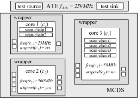
Figure 1. Multi-clock domain SoC.
a test scheduling problem for multi-clock domain SoCs in Section 4, we present a power-constrained test scheduling algorithm in Section 5. Experimental results are discussed in Section 6. Finally, Section 7 concludes this paper.
2 Multi-Clock Domain SoCs
This section describes the formal notation we use to model the multi-clock domain SoC under test. An ex- ample of an SoC is shown in Figure 1 where each core is wrapped to ease test access. Test pattern source and test response sink are implemented off-chip as an ATE. The SoC can be modeled as a multi-clock domain SoC, M CDS = (C, R, Pmax), where:
C = {c1, c2, ..., cn} is a set of cores; Each coreciis characterized by:
f req(ci): maximum test frequency of core ci∈ C; power(ci): power consumption of core ci∈ C at test
frequencyf req(ci);
atspeed: C → {yes, no}: at-speed test requirement R = {R1, R2, ..., Rn} is a set of wrapper lists;
Each wrapper listRiis characterized by:
Ri= {ri1, ri2, ..., rij} is a set of wrapper designs for coreci;
Each wrapper designrijis characterized by: pin(rij): number of pins to test core ciwithj-
th wrapper design ;
cycle(rij): number of clock cycles to test core ciwithj-th wrapper design;
Pmax: maximum allowed power at any time;
We consider that an SoC consists of the maximum al- lowed power consumption and cores working at different test frequencies. However, we assume that each core has been designed with single-clock domain during test. For each core, a maximum test frequency and a power consump- tion at the given maximum frequency are given. Each core also has an information about the requirement of at-speed testing. atspeed(ci) = yes means that cimust operate at f req(ci) during test (i.e., we cannot change the test fre- quency ofcifor test scheduling).atspeed(ci) = no means thatcican be tested at lower frequencies thanf req(ci) (i.e., we can decrease the test frequency of ci for test schedul- ing). Moreover, each core has a wrapper list that consists of possible wrapper designs for the core. Each wrapper de-
Figure 2. Test data multiplexing/de-multiplexing.
sign has a number of test pins and a number of clock cy- cles required to test the core with the wrapper design. The test time for ci working atf req(ci) can be calculated as cycle(ci) / f req(ci).
3 Virtual TAM for Power Minimization
The frequency gaps between ATE and cores can be solved by using virtual TAM techniques based on band- width matching. Whenf req(ci) (clock frequency of core ciduring test) is higher thanfAT E(clock frequency of ATE) (Fig. 2(a)), we insert a TDM (test data multiplexing) cir- cuit between ATE outputs and the core inputs, and mul- tiplex ⌈f req(ci)/fAT E⌉ · m TAM wires at fAT E intom virtual TAM wires at f req(ci). On the other hand, when f req(ci) is lower than fAT E (Fig. 2(b)), we insert a TD- deM(test data de-multiplexing) circuit between ATE output and the core inputs, and de-multiplexn TAM wires at fAT E
into⌊n · fAT E/f req(ci)⌋ virtual TAM wire at f req(ci). To observe test responses, we need to insert TDM/TDdeM be- tween the core output and ATE inputs in the similar fashion. In this paper, we also utilize virtual TAM technique to reduce power consumption of a core while maintaining the same test time of the core. The dynamic powerP (k) (which is the dominant source of power consumption in CMOS cir- cuits) consumed in the circuit on application of consecutive two test vectors(Vk−1, Vk) is as follows [23].
P (k) = 1/2 · f · VDD2 ·!Ci· Si(k) (1) Here, f is the clock frequency, VDD is the power supply voltage,Ciis the output capacitance at nodei and Si(k) is the number of switchings provoked byVkat nodei. From the equation(1), we observe that the power consumption of a core during test can be reduced by lowering its test fre- quency. However, this increases test time of the core pro- portionally to the power reduction ratio. Here, we insert TDdeM circuit between the ATE outputs and the core in- puts. Then, more virtual TAM wires become available for the core, and test time can be reduced. In the best case, we can achieve the same test time with 50% reduction of power consumption for a core by using the above power-conscious virtual TAM technique. For example, we consider the wrap-
Table 1. Power-conscious virtual TAM for core7 in d695.
frequency(MHz) # virtual TAM wires test time(µs) # cycles
50 10 264.86 13243
25 20 268.68 6717
per design for core7 in d695 from ITC’02 SoC benchmarks [24]. Table 1 shows that we can achieve a 50% power re- duction with an 1.4% test time overhead by decreasing the frequency from 50MHz to 25MHz and increasing the num- ber of virtual TAM wires from 10 to 20.
4 Problem Formulation
We formulate the power-constrained test scheduling problem for multi-clock domain SoCsPmcds that we ad- dress in this paper as follows.
Definition 1 Pmcds: Given a multi-clock domain SoC M CDS, the number of available test pins Wmaxand the clock frequency of ATEfAT E, is there a test schedule for M CDS that satisfies all the following conditions?
1. the total number of test pins used at any moment does not exceedWmax,
2. the total power consumption used at any moment does not exceedPmax,
3. each core satisfies at-speed test requirement (i.e., if atspeed(ci) = yes, ci must be tested at f req(ci). Otherwise,cican be tested at frequencies lower than f req(ci)),
4. the overall SoC test time is minimized
If there is such a test schedule, determine a wrapper design and test frequency of each core for the test schedule.
5 Scheduling Algorithm
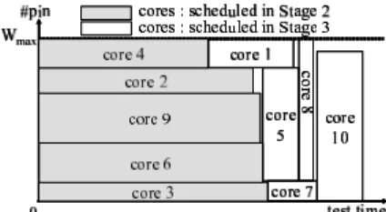
This section presents a heuristic algorithm forPmcdsthat consists of the following three stages: 1) testability analy- sis, 2) test scheduling at time 0 for cores with large amount of test data, and 3) test scheduling based on Best Fit De- creasing (BFD) heuristic [25] for remaining cores. The ex- ample of the generated test schedule is shown in Figure 3. The shaded cores and the unshaded cores in Figure 3 are scheduled in stage 2 and stage 3, respectively. The follow- ing subsections describe the details of each stage.
5.1 Testability Analysis (Stage 1)
If M CDS cannot satisfy the following two conditions for the given parameters:fAT EandWmax, then there is no solution forPmcds.
For eachci∈ C such that atspeed(ci) = yes, [power limitation]
Pmax≥ power(ci) (2)
[pin limitation] Wmax≥ min
j (pin(rij)) · ⌈f req(ci)/fAT E⌉ (3) For a corecisuch thatatspeed(ci) = yes, we cannot change the test frequency f req(ci) and power consump- tion power(ci) during test. Therefore, the core that can-
Figure 3. A test schedule example.
not satisfy equation(2) exceeds a given power limitation even if it is tested alone. Moreover, as explained before, TDM/TDdeM circuits can be uniquely determined when fAT E, a wrapper designrijand a test frequency forciare given. Therefore, the core that doesn’t satisfy equation(3) cannot be assigned enough wrapper pins to achieve at-speed test atf req(ci).
5.2 Test scheduling at time 0 with minimum test frequency (Stage 2)
This stage consists of the following three steps. Step 1: determine a wrapper design and test frequency for each core
Main idea in this step is to increase test concurrency for power-constrained test scheduling by lowering the test fre- quencies of cores which do not require at-speed test. For each core ci, we determine a wrapper design rtesti and a multiplicitymcisuch that
1. TLB≥ cycle(rtesti )/(f req(ci)/mci), 2. pin(rtesti ) ≤ Wmax· fAT E/(f req(ci)/mci), 3. pin(rtesti ) is maximized, and
4. mciis maximized.
Here, lower boundTLB on the SoC test time is defined as follows.
TLB= max{max
i (T ci
LB), T otalData/(Wmax· fAT E)} (4) Lower boundTLBci on the core test time andT otalDate are defined as follows.
TLBci = cycle(rij)/f req(ci) s.t. 1.pin(rij) is maximized, and
2.pin(rij) ≤ Wmax· fAT E/f req(ci). (5) T otalData =!
i
pin(rij) · cycle(rij) s.t.
pin(rij) is minimized. (6)
Then, we determine test frequency fctesti for ci as fol- lows.
fctesti =
"
f req(ci)/mci ifatspeed(ci) = no
f req(ci) ifatspeed(ci) = yes (7) Step 2: determine cores which start their tests at time 0
First, we sort cores in the descending order based on its TLBci . Then, we schedule a coreciin the above order at time 0 with wrapperrtesti and test frequencyfctesti . This process repeats until 1) the power consumption at time 0 (P0) does not exceedPmax, 2) the pin usage at time 0 (W0) does not
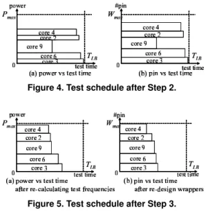
Figure 4. Test schedule after Step 2.
Figure 5. Test schedule after Step 3.
exceedWmax, and 3)TLBci is less thanTLB/|C|. Here, |C| denotes the number of cores in the SoC. The third condition can prevent us from scheduling cores with small amount of test data to time 0. Instead of scheduling such small cores at time 0, Step 3 re-designs wrappers and re-calculates test frequencies for the cores scheduled in this step to reduce the overall test time of the SoC.
Figure 4 shows a current test schedule generated after Step 2. In Figure 4(a), the horizontal axis denotes the test time, and the vertical axis denotes the power consumption used in each test time. In Figure 4(b), the horizontal axis de- notes the test time, and the vertical axis denotes the number of test pin used in each test time.
Step 3: re-calculate test frequencies and re-design wrap- pers for cores scheduled at time 0
There exists a case whereP0(power consumption at time 0) does not reachPmaxafter Step 2 (Fig. 4(a)) since Step 2 stops the above three conditions. In this case, we find a core cithat satisfies all the following conditions.
1. cycle(ritest)/fctesti is maximized (8)
2. mci> 1 (9)
3. Pmax≥ P0− power(ci){1/mci+ 1/(mci− 1)}(10) 4. Pmax/2 ≥ power(ci)/(mci− 1) (11) If there exists such a coreci, we updatemcitomci− 1, and reduce the test time of ciby increasingfctesti accord- ing to equation (7). The fourth condition (equation(11)) can prevent one core from dominating power consumption, and help us to increase the test concurrency at time 0. This pro- cess repeats until 1)P0does not exceedPmaxand 2) there exists a core that satisfies the above conditions. Figure 5(a) shows a result where we apply this process to the current schedule generated after Step 2 corresponds to Figure 4. In this figure, frequencies for core 2, 3, 4 and 6 are increased. Consequently, the test time for these cores are reduced.
Figure 6. An example of test scheduling for core 5. Similarly, there exists a case whereW0(pin usage at time 0) does not reachWmaxafter Step 2. In this case, we find a coreciwith maximum test time, then assign 1 test pin to ci. This process repeats untilW0does not exceedWmax. Figure 5(b) shows a result where we apply this process to the current schedule corresponding to Figure 5(a).
5.3 Test scheduling for remaining cores based on BFD (Stage 3)
In this stage, we determine a test schedule for the remain- ing cores based on BFD heuristic. First, we pick a coreciin the descending order based onTLBci . Then, we find the best start time, wrapper design and test frequency forcisuch that the total test time of the given SoC is minimized as follows. 1. LetS be a set of start time candidates that consists of the end time of scheduled cores in the current sched- ule. For each candidates ∈ S, we calculate available power consumptionPsand available test pinWsfrom the current schedule.
2. For each candidates ∈ S,
(a) Determine a maximum test frequencyfctesti,s such
thatpower(ci) · fctesti,s/f req(ci) does not exceed Ps.
(b) Determine a wrapper design ri,stest such that 1) pin(rtesti,s ) does not exceed Ws· fAT E/fctesti,s and 2)pin(ri,stest) is maximized.
(c) Calculate the end timeti,swhencistarts its test at times with wrapper rtesti,s at frequencyfctesti,s.
3. Scheduleciat times with wrapper rtesti,s at frequency fctesti,s such that 1)ti,sis minimized and 2) the test ofci
does not overlap the tests of cores already scheduled in the current schedule.
Figure 6 shows an example of the test scheduling for core 5. Here, a set of start time candidates S consists of five elements: s1, s2, s3, s4, s5. For each candidates ∈ S, we calculate a end time t5,s by determining a test frequency fctest5,s and a wrapper design rtest5,s shown as a rectangle in Figure 6. In this example, core 5 is scheduled to start its test at times4with a wrapperrtest5,4 at frequencyfctest5,4 since the end timet5,4has a minimum value.
This process repeats until all the remaining cores are scheduled in the descending order based onTLBci . Through the above processes, we can generate a final test schedule.
6 Experimental Results
In Section 6.1, we show experimental results for a multi- clock domain SoC with power constraint. Section 6.2 presents experimental results for single-clock domain SoCs with power constraint (“d695” and “h953” from ITC’02 SoC benchmarks [24]) in order to show the effectiveness of our approach compared to previous works. All the experi- mental results can be obtained within 0.1 sec. on a SunBlade 2000 workstation (1.05 GHz with 8GB RAM).
6.1 Results for a multi-clock domain SoC
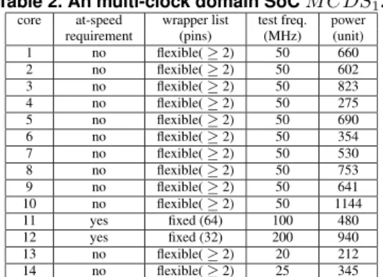
Since there exists no approach that has tackled the test scheduling problem for multi-clock domain SoCs, it is dif- ficult to compare with previous works. We have decided to analyze the trade-offs of the proposed method in terms of the number of available test pin, the clock frequency of ATE, maximum allowed power consumption and test time for a hypothetical multi-clock domain SoC. Table 2 shows the multi-clock domain SoCM CDS1used in this exper- iment. This SoC consists of 14 cores. First 10 cores are from “d695” in ITC’02 SoC benchmarks. “flexible(≥ 2)” in column “wrapper list” denotes that we can design any wrapper (wrapper with any number of test pins) by the pro- cedure proposed in [2, 3]. We use the same power con- sumption shown in [15], and assume that f req(ci) = 50 MHz andatspeed(ci) = no for these 10 cores. The wrap- pers for core 11 and core 12 are already designed (i.e., 64 pins, 32 pins, respectively). We assume that these two cores are tested at higher frequencies than other cores, and atspeed(ci) = yes. Core 13 and core 14 are copies of core 7 and core 5, respectively. However, we assume that these two cores are tested at lower frequencies than other cores.
For this SoC, Table 3 shows test time results whenfAT E
= 200MHz, 100MHz and 50MHz. In this table, the test time results are shown as “µsec.”, and “untestable” denotes that there exists no solution for the given parameters. In this SoC, since core 11 should be tested at 100MHz with 64 pins, we observe that there exists no solution for three cases: 1)fAT E= 100MHz andWmax= 32, 2)fAT E= 50MHz and Wmax= 32, and 3)fAT E= 50MHz andWmax= 64. We also observe that test time depends on the product offAT E
and Wmax. Therefore, when we use a high speed ATE, we can test SoCs with small number of test pins. On the other hand, even when we use a low speed ATE, we can achieve the same test time by using more test pins. From this results, the designer can decide the number of test pins and the speed of the test pin considering the total cost for them.
6.2 Comparison with other approaches
The proposed test data de-multiplexing technique is also effective for the power-constrained test scheduling of the single-clock domain SoCs as well as for that of the multi- clock domain SoCs. In order to show the effectiveness of
Table 2. An multi-clock domain SoCM CDS1.
core at-speed wrapper list test freq. power requirement (pins) (MHz) (unit)
1 no flexible( ≥ 2) 50 660
2 no flexible( ≥ 2) 50 602
3 no flexible( ≥ 2) 50 823
4 no flexible( ≥ 2) 50 275
5 no flexible( ≥ 2) 50 690
6 no flexible( ≥ 2) 50 354
7 no flexible( ≥ 2) 50 530
8 no flexible( ≥ 2) 50 753
9 no flexible( ≥ 2) 50 641
10 no flexible( ≥ 2) 50 1144
11 yes fixed (64) 100 480
12 yes fixed (32) 200 940
13 no flexible( ≥ 2) 20 212
14 no flexible( ≥ 2) 25 345
our approach compared to previous works, we present ex- perimental results for the single-clock domain SoCs with power constraint. We use “d695” and “h953” from ITC’02 SoC benchmarks [24] as the single-clock domain SoCs by assuming thatfAT E = 50 MHz, and f req(ci) = 50 MHz and atspeed(ci) = no for all core ci ∈ C. This is be- cause only these two SoCs have power information in the benchmarks (for “d695”, we use the same power consump- tion shown in [15]). Table 4 shows the test time results of the proposed method and the previous power-constrained approaches [15, 16] which are applicable only to the single- clock domain SoCs. In this table, test time results are shown as the number of clock cycles. “NA” denotes that the ap- proach is not applicable for the constraint. “-” denotes that no result is shown for the constraint in the approach. For d695, we observe that the proposed approach can achieve a 6.9% reduction in average test time compared to [15]. Moreover, for h953, we observe that the proposed approach can achieve the lower bound (119357) on the SoC test time [14] under all power constraints. From these results, we conclude that the proposed power-conscious virtual TAM technique and test scheduling algorithm are also effective for single-clock domain SoCs.
7 Conclusions
This paper has presented a power-conscious wrapper and TAM design for multi-clock domain SoCs, and proposed a test scheduling algorithm to minimize test time under power constraint. To the best of our knowledge, a test scheduling problem for multi-clock domain SoCs has been addressed and formulated for the first time in this paper. Moreover, we have presented a technique to reduce power consump- tion of a core during test while maintaining the test time by utilizing virtual TAM technique which is applicable to both single and multi clock domain SoCs.
Acknowledgments
This work was supported in part by Japan Society for the Promotion of Science (JSPS) under Grants-in-Aid for Sci- entific Research B(2)(No. 15300018). The authors would like to thank Prof. Kewal K. Saluja, Michiko Inoue, Dr.
Table 3. Test time results [µs] for multi-clock domain SoCM CDS1.
fAT E=200MHz fAT E=100MHz fAT E=50MHz
Pmax Wmax Wmax Wmax
32 pin 64 pin 128 pin 32 pin 64 pin 128 pin 32 pin 64 pin 128 pin 1500 431.05 351.22 351.22 untestable 431.05 351.22 untestable untestable 431.05 2000 325.29 278.55 278.55 untestable 325.29 278.55 untestable untestable 325.29 2500 324.05 234.24 221.70 untestable 324.05 234.34 untestable untestable 324.05
Table 4. Test time results (# cycles) for single-clock domain SoCs.
Wmax
SoC Pmax 32 pin 64 pin 128 pin
3D[15] EA[16] proposed 3D[15] EA[16] proposed 3D[15] EA[16] proposed
d695 1000 NA NA 44528 NA NA 27482 NA NA 24707
1500 45560 - 42981 27573 - 22690 16841 - 16239
2000 43221 - 42632 24171 - 21838 14128 - 12753
2500 43221 - 42564 23721 - 21616 12993 - 11180
h953 5× 10⁹ NA NA 119357 NA NA 119357 NA NA 119357
6× 10⁹ 122636 122636 119357 122636 122636 119357 122636 122636 119357 7× 10⁹ 119357 119357 119357 119357 119357 119357 119357 119357 119357
Satoshi Ohtake and members of Fujiwara Laboratory (Nara Institute of Science and Technology) for their valuable com- ments.
References
[1] Y. Zorian, E. J. Marinissen and S. Dey,“Testing embedded-core based system chips,” Proc. 1998 Int. Test Conf., pp. 130–143, Oct. 1998. [2] V. Iyengar, K. Chakrabarty and E. J. Marinissen, “Test Wrapper and
test access mechanism co-optimization for system-on-chip,” Journal of Electronic Testing: Theory and Applications, pp. 213–230, Apr. 2002.
[3] W.Zou,S.R.Reddy,I.Pomeranz and Y.Huang,“SOC Test Scheduling Using Simulated Annealing,” Proc. 21th VLSI Test Symp.,pp.325– 329,May 2003.
[4] E. J. Marinissen, S. K. Goel, and M. Lousberg, “Wrapper Design for Embedded Core Test,” Proc. IEEE International Test Conference (ITC), pp. 911–920, Oct. 2000.
[5] E.J. Marinissen, R. Kapur, M. Lousberg, T. McLaurin, M. Ric- chetti and Y. Zorian, “On IEEE P1500’s Standard for Embedded Core Test,” Journal of Electronic Testing: Theory and Applications, pp.365–383, Aug. 2002.
[6] T. Ono, K. Wakui, H. Hikima, Y. Nakamura and M. Yoshida, “Inte- grated and automated design-for-testability implementation for cell- based ICs,” Proc. 6th Asian Test Symp., pp. 122–125, Nov. 1997. [7] P. Varma and S. Bhatia, “A structured test re-use methodology for
core-based system chips,” Proc. 1996 Int. Test Conf., pp. 294–302, Oct. 1998.
[8] E. Marinissen, R. Arendsen, G. Bos, H. Dingemanse, M. Lousberg and C. Wouters, “A structured and scalable mechanism for test access to embedded reusable cores,” Proc. 1998 Int. Test Conf., pp. 284– 293, Oct. 1998.
[9] M. Nourani and C. A. Papachristou, “Structural fault testing of em- bedded cores using pipelining,” Journal of Electronic Testing:Theory and Applications 15(1-2), pp. 129–144, Aug.–Oct. 1999.
[10] S. Ravi, G. Lakshminarayana, and N. K. Jha, “ Testing of core-based systems-on-a-chip,” IEEE Trans. on CAD, Vol. 20, No. 3, pp. 426– 439, Mar. 2001.
[11] T. Yoneda, T. Uchiyama and H. Fujiwara, “Area and time co- optimization for system-on-a-chip based on consecutive testability,” Proc. 2003 Int. Test Conf., pp. 415–422, Sep. 2003.
[12] Y.Huang et al.,“Resource allocation and test scheduling for con- current test of core-based SOC design,”Proc. Asian Test Sympo- sium(ATS), pp265-270, 2001.
[13] V. Iyengar, K. Chakrabarty and E. J. Marinissen, “On using rectangle packing for SOC wrapper/TAM co-optimization,” Proc. 20th VLSI Test Symp., pp. 253–258, Apr. 2002.
[14] S. K. Goel and E. J. Marinissen,“Effective and Efficient Test Ar- chitecture Design for SOCs,”Proc. IEEE International Test Confer- ence(ITC), pp529-538, 2002.
[15] Y. Huang, N. Mukherjee, S. Reddy, C. Tsai, W. Cheng, O. Samman, P. Reuter and Y. Zaidan, “Optimal core wrapper width selection and SOC test scheduling based on 3-dimensional bin packing algorithm,” Proc. 2002 Int. Test Conf., pp. 74–82, Oct. 2002.
[16] Y. Xia, M. C. Jeske, B. Wang and M. Jeske, “Using Distributed Rect- angle Bin-Packing Approach for Core-based SoC Test Scheduling with Power Constraints, ” ICCAD’03, pp.100–105, Nov. 2003. [17] E. Larsson, K. Arvidsson, H. Fujiwara and Z. Peng,,“Efficient Test
Solutions for Core-based Designs,”IEEE Trans. on CAD, Vol. 23, No. 5, pp. 758–775, May 2004.
[18] A.Khoche,“Test resource partitioning for scan architectures using bandwidth matching,”Digest of Int. Workshop on Test Resource Partitioning,pp.1.4-1–1.4-8, 2001.
[19] A.Sehgal,V. Iyengar,M.D.Krasniewski and K. Chakrabarty, “Test Cost Reduction for SOCs Using Virtual TAMs and Lagrange Multi- pliers,” In Proc.IEEE/ACM Design Automation Conference,pp.738– 743,Jun.2003.
[20] Q.Xu and N.Nicolici, “Wrapper Design for Testing IP Cores with Multiple Clock Domains,” In Proceedings of the 2004 De- sign,Automation and Test in Europe(DATE),pp.416–421,Feb.2004. [21] Q. Xu, N. Nicolici and K. Chakrabarty, “Multi-frequency wrapper
design and optimization for embedded cores under average power constraints”, Proc. IEEE/ACM Design Automation Conference, pp. 123-128, 2005.
[22] Q.Xu and N.Nicolici, “Multi-frequency Test Access Mechanism De- sign for Modular SOC Testing,”Proc. of IEEE the 13th Asian Test Symposium, pp.2–7, Nov. 2004.
[23] P. Girard, “Survey of low-power testing of VLSI circuits,” IEEE De- sign & Test of Computers, Vol. 19, No. 3, pp. 82–92, May–June 2002. [24] E. J. Marinissen, V. Iyengar and K. Chakrabarty, “A Set of Bench- marks for Modular Testing of SOCs,” Proc. IEEE International Test Conference (ITC), pp. 519–528, Oct. 2002.
[25] M. R. Garey and D. S. Johnson, Computers and Intractability: A Guide to the Theory of NP-Completeness, San Francisco, CA: W. H. Freeman and Co., 1979.
![Table 3. Test time results [ µ s] for multi-clock domain SoC M CDS 1 . f AT E = 200MHz f AT E = 100MHz f AT E = 50MHz](https://thumb-ap.123doks.com/thumbv2/123deta/5752906.27068/6.892.165.704.183.422/table-test-results-multi-clock-domain-mhz-mhz.webp)
