A Non-Scan Approach to DFT for Controllers Achieving
100% Fault Efficiency
SATOSHI OHTAKE, TOSHIMITSU MASUZAWA AND HIDEO FUJIWARA
Graduate School of Information Science, Nara Institute of Science and Technology, 8916-5, Takayama, Ikoma, Nara 630-0101, Japan
[email protected] [email protected]
Received June 4, 1999; Revised August 3, 2000 Editor: S. Demidenko
Abstract. This paper presents a non-scan design-for-testability method for controllers that are synthesized from FSMs (Finite State Machines). The proposed method can achieve complete fault efficiency: test patterns for a combinational circuit of a controller are applied to the controller using state transitions of the FSM. In the proposed method, at-speed test application can be performed and the test application time is shorter than previous methods. Moreover, experimental results show the area overhead is low.
Keywords: non-scan design for testability, complete fault efficiency, controllers, at-speed test
1. Introduction
Testing of large VLSI circuits is a well-known hard problem. It is necessary to reduce the cost of testing and to enhance the quality of testing. The cost of testing is estimated by test generation time and test applica- tion time. The quality of testing is estimated by fault efficiency.1 Therefore, we have to reduce test genera- tion time and test application time and to enhance fault efficiency.
For combinational circuits, efficient test generation algorithms are proposed [1] to generate test patterns and complete (100%) fault efficiency can be achieved. On the other hand, for sequential circuits, ordinary test generation algorithms generally can not attain com- plete fault efficiency within reasonable time since the search space of test generation grows explosively as the number of flip-flops (FFs) increases. Therefore, sev- eral design-for-testability (DFT) methods for sequen- tial circuits are proposed.
One of the most commonly used DFT methods for sequential circuits is the full-scan DFT method [1]. A sequential circuit consists of a combinational logic block and a state register (set of FFs). In order to con- trol and to observe the value of the state register, the full-scan DFT method replaces each FF in the state register with a scannable FF. By considering the state register as primary inputs/outputs, a combinational test generation algorithm can be used to obtain a test se- quence with short test generation time and to achieve complete fault efficiency. However, as the number of FFs of the state register becomes larger, test applica- tion time becomes longer because of scan in/out opera- tions. Furthermore, this method excludes at-speed test application (test application at the operational speed). Maxwell et al. [2] show that the number of physi- cal faults detected by applying test patterns for stuck- at faults at the operational speed is larger than that at slow speed. Therefore, at-speed test application is important.
test generation algorithm must be used.
Finite state machine (FSM) based non-scan DFT ap- proaches are also proposed. In [4], a method to aug- ment an arbitrary FSM to an easily testable FSM by adding two special input symbols and an efficient pro- cedure to construct a checking experiment for the aug- mented FSM are proposed. This method is based on checking experiments and focuses only state transition checking.
A DFT method for PLA-based FSMs is proposed in [5]. In this method, the output and state equations of a FSM are modified to incorporate a scan-like function in a PLA. In this method, test application time is long due to scan-like operation.
FSM synthesis for testability methods are proposed in literature [6] and [7]. In these methods, given an FSM, to make memory elements fully control- lable/observable, test functions are embedded to the given FSM. Therefore these approaches can apply a combinational test generation algorithm to a synthe- sized circuit of the augmented FSM. Test application time of these methods is long because state initializa- tion and distinguishing sequence are required for each test pattern of the circuit. In [8], a method which is similar to these method for PLAs is proposed. In this method, given an FSM, fault tolerant test functions are embedded to the given FSM and then the test functions are not disabled by some fault in a synthesized circuit of the augmented FSM.
Synthesis for testability method for FSMs based on strong-connectivity is proposed in [9]. This method can improve connectivity of state diagrams and hence can improve testability of synthesized circuits of the aug- mented state diagrams.
In this paper, we present a new non-scan DFT method for controller circuits of VLSIs which guaran- tees complete fault efficiency. In general, a controller
valid states. Moreover, in order to observe responses of the combinational logic block, we append observation points (additional test output pins) in front of the state register. Partial scan approaches to set those invalid states to state register are proposed in [10–12]. How- ever, these approaches require a sequential test gener- ation algorithm and complete fault efficiency can not always be achieved. Furthermore, in these approaches, test application time is long and at-speed testing can not be performed. Although our proposed method has the following advantages:
1. Test patterns can be generated by combinational test generation algorithms.
2. Complete fault efficiency can be achieved.
3. Test application time is shorter than previous methods.
4. At-speed testing can be performed.
In this paper, we also evaluate the effectiveness of the proposed method by experiments with MCNC’91 FSM benchmarks. The experimental results show that the proposed method is effective and the area overhead is low.
This paper is organized as follows: Section 2 gives some definitions. Section 3 describes an overview of our approach. Section 4 presents a non-scan DFT method for controllers. Section 5 presents a test gener- ation method and a test application method. Section 6 shows comparison of the proposed method with previ- ous methods and presents experimental results.
2. Preliminaries
In register transfer level (RTL) description, a VLSI cir- cuit generally consists of a controller and a data path.
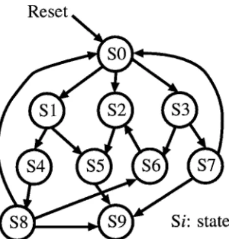
Fig. 1. A finite state machine (FSM).
In this paper, we consider only controllers. A controller is described by a finite state machine (FSM). An FSM (see Fig. 1) has one reset state, and it goes to the reset state regardless of the current state when reset signal is supplied. A controller is realized by a sequential cir- cuit (see Fig. 2) which is synthesized from an FSM by logic synthesis. A sequential circuit consists of a com- binational logic block (CC) and a state register (SR). In the logic synthesis, a state assignment is determined to assign a value of the SR to each state of the FSM. In this paper, for simplicity, we assume that only a single value is assigned to each state. This assumption makes no restriction on sequential circuits under consideration. Even if the case that two or more values are assigned to one state for a sequential circuit, our method can be applied to the sequential circuit by regarding those values as different states of the FSM.
Let n be the number of FFs in the SR of a sequen- tial circuit synthesized from an FSM. Then the SR can
Fig. 2. A sequential circuit.
represent 2n states which can be classified into valid states and invalid states as follows.
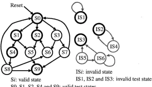
Definition 1. For any value of the SR in a sequential circuit synthesized from an FSM, if the corresponding state of the value is reachable from the reset state, then the state is called a valid state (see Fig. 3). Otherwise, the corresponding state is called an invalid state.
In this paper, we consider testing of the combina- tional logic block in a sequential circuit under the single stuck-at fault model. In order to guarantee complete fault efficiency, we first extract a combinational test generation model from a given sequential circuit, and then generate test patterns for the combinational test generation model. The combinational test generation model is defined as follows.
Definition 2. For a sequential circuit (Fig. 2), a com- binational circuit extracted from the sequential circuit by replacing the SR with pseudo primary inputs and pseudo primary outputs is called a combinational test generation model (Fig. 4).
Each test pattern for the combinational test genera- tion model consists of two values; one corresponding to primary inputs (PIs) and the other corresponding to pseudo primary inputs (PPIs). We classify those test patterns into two classes as follows.
Definition 3. If the value of PPIs of a test pattern is a valid state, the test pattern is called a valid test pattern. Otherwise, the test pattern is called an invalid test pattern. A valid state that appears in some valid test pattern is called a valid test state, and an invalid
Fig. 3. Valid states and invalid states.
Fig. 4. A combinational test generation model.
state that appears in some invalid test pattern is called an invalid test state (see Fig. 3).
3. Overview
In this section, we give an overview of our non-scan DFT method.
For a sequential circuit synthesized from an FSM, our method achieves complete fault efficiency with short test generation time and allows at-speed test. In order to generate a test sequence and achieve complete fault efficiency with short test generation time, we gen- erate test patterns for the combinational test generation model of the sequential circuit using a combinational test generation algorithm. Each of test patterns con- sists of the values of primary inputs (PIs) and pseudo primary inputs (PPIs). In order to apply a test pattern to the combinational logic block, we have to set the value
of PPIs of the test pattern to the SR of the sequential circuit. If the value corresponds to a valid state (i.e., the test pattern is a valid test pattern), the value of PPIs can be set to the SR using original state transitions of the FSM.
On the other hand, if the value corresponds to an invalid state (i.e, the test pattern is an invalid test pat- tern), the value of PPIs can not be set to the SR using state transitions of the FSM. In order to set the invalid state to the SR, we append an extra logic which gener- ates all invalid test states to the synthesized sequential circuit. In order to observe responses of the combina- tional logic block, we also append observation points (additional test output pins) in front of the SR. Note that we just append the extra logic but do not change the combinational logic block. This guarantees complete fault efficiency.
We show details of the non-scan DFT method in Section 4 and the corresponding test generation method and test application method in Section 5.
4. Design for Testability
In this section, we propose a non-scan DFT method for controllers.
4.1. Processes of DFT
We assume that a controller is given as an FSM. A non-scan DFT method for a controller consists of the following five steps.
Step 1: Logic synthesis. Given an FSM, we synthesize a sequential circuit from the FSM. Here, we assume that the information of the state assignment can be utilized in the following steps.
Step 2: Combinational test generation. From the syn- thesized sequential circuit, we extract the combi- national test generation model. Then, we generate test patterns for the combinational test genera- tion model using a combinational test generation algorithm.
Step 3: Extracting invalid test states. We classify the test patterns generated at the previous step into valid test patterns and invalid test patterns and obtain a set of valid test states and that of invalid test states. Step 4: Appending an extra logic. If the set of invalid
test states is not empty, we append an extra logic that can set all invalid test states to the SR as follows. Otherwise, we skip to Step 5.
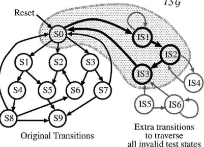
Step 4.1: Synthesizing ISG. We synthesize a combi- national logic called an invalid test state generator ISG that can generate all invalid test states as fol- lows. First, we generate an FSM that can traverse all invalid test states from the reset state of the given FSM (see Fig. 5). The traversing order and the input values causing these transitions can be determined arbitrarily. We can achieve complete fault efficiency despite of them while the amount of hardware overhead depends on them. Then, the ISG is synthesized from the generated FSM.
Fig. 5. An FSM traversing invalid test states.
Notice that, the state assignment of these invalid test states is already determined at Step 1 and Step 2.
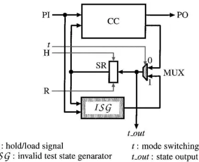
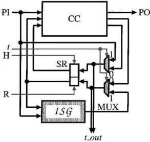
Step 4.2: Appending ISG. The ISG generated above is appended to the sequential circuit synthesized at Step 1 with a multiplexer (MUX), a mode switch- ing signal t and state output signals t out (Fig. 6). The mode switching signal t controls the MUX and is set to one only when an invalid test state must be set to the SR during test. The state output signals t out is used to observe the responses of test patterns.
The SR of the sequential circuit can represent 2n (n: the number of FFs of the SR) states. The num- ber of invalid test states is at most the number of test patterns. It is conceivable that the number of invalid test states is much smaller than that of states represented by the SR. Thus we expect that the test application time does not become long and the hard- ware overhead caused by the extra logic is not high. The transitions to invalid test states are used only during test application. Therefore, we can append the extra logic to the synthesized sequential circuit without changing the combinational logic block. Step 5: Adding hold mode to the state register. Finally,
we add hold mode to the SR (Fig. 6). This hold mode is utilized to reduce test application time. We give the details in Section 5. The hold mode can be implemented by one of the following ways.
Fig. 6. A controller augmented with an invalid test state generator.
Fig. 7. Implementations of hold mode.
1. The most commonly used implementation of the hold mode is appending an MUX in front of the SR (Fig. 7(a)). The hold/load signal is connected to the address line of the MUX and selects the next state or the present state of the SR.
2. The hold mode is implemented by appending an AND gate to the clock port of the SR (Fig. 7(b)). The inputs of the AND gate is the clock signal of the controller and the hold/load signal. The clock signal is masked if the hold/load signal is zero. While we assume a controller is given as an FSM, this assumption makes no restriction on controllers un- der consideration. Even in the case that a controller is given as a gate-level circuit, this method can be applied by extracting an FSM from the circuit using a state ma- chine extraction algorithm (e.g. one available in SIS [13]).
Example 1. Given an FSM of Fig. 1, we apply this DFT method. The FSM has 10 states from S0 to S9. First, we synthesize a sequential circuit of Fig. 2 from the FSM. The sequential circuit has an SR which con- sists of 4 FFs. The SR represents 16 states (Fig. 3): 10 valid states (from S0 to S9) and 6 invalid states (from IS1 to IS6). Second, we obtain the combinational test generation model of Fig. 4 from the sequential circuit and generate test patterns of the combinational test gen- eration model using a combinational test generation algorithm. In the third step of our DFT, we classify these test patterns into valid test patterns and invalid test patterns and obtain sets of valid test states and invalid test states (Fig. 3). The set of valid states is {S0, S1, S2, S4, S9} and the set of invalid test states is {IS1, IS2, IS3}. Then, we design an ISG which implements the transitions S0→IS1→IS2→IS3→S0 (Fig. 5) and append the ISG to the sequential circuit
with an MUX (Fig. 6). Finally, we add hold mode to the SR.
4.2. Delay Overhead
For a sequential circuit (a controller), the proposed DFT method appends an MUX in front of the SR and add hold mode to the SR. Thus, a delay overhead is caused at normal operation of the controller due to the MUX and an extra logic for hold mode of the SR. However, the delay overhead is the same as the full-scan DFT method. Moreover, controllers can be designed and synthesized with taking the delay overhead into con- sideration because the delay overhead can be estimated at the first step of designing controllers.
On the other hand, an ISG gives no affect to the nor- mal operation of a controller. If we can synthesize the ISG with shorter delay than the combinational logic block, we can perform test application at the normal operation speed.
4.3. Area Overhead
For a sequential circuit (a controller), the proposed DFT method has an area overhead due to the ISG, the MUX, and an extra logic for hold mode of the SR. The areas of the MUX and the extra logic are the same as that of the full-scan DFT method. This method appends the ISG which generates the invalid test states to the sequential circuit. The order of the invalid test states generated by the ISG does not affect fault efficiency. However, it is conceivable that the order affects the area of the ISG. Therefore, we can minimize the area overhead by considering the appropriate order of the invalid test states.
If we design a sequential circuit as shown in Fig. 8, we can control the values of some FFs in the SR directly from primary inputs. In this case, only the values of the FFs which can not be controlled directly from primary inputs have to be generated by the ISG, and thus, the number of invalid states generated by the ISG are re- duced. Therefore, the area of the ISG can be reduced.
4.4. Observation Points
We suppose that t out shown in Figs. 6 and 8 is an observation point for testing. Thus primary output pins for t out are required. However, due to limitation of the number of primary output pins, we may not use
Fig. 8. An example of invalid test state generation using primary inputs.
sufficient primary output pins for t out. An RTL circuit generally consists of a controller and a data path. When testing the controller, the data path is not used. Hence we can use the primary output pins of the data path as the observation points of the controller. Thus, t out can be observed at the primary output pins of the data path by inserting an extra MUX in front of the primary output pins. In the case when the data path does not have sufficient primary output pins, we can observe a parity of t out using an XOR tree. If an error of a fault is observed at an odd number of t out, the fault can be detected. If an error of a fault is observed at an even number of t out, the fault can not be detected. Fujiwara et al. [14] show that, for most faults, an error of a fault is observed at an odd number of outputs by experiments with ISCAS’89 benchmarks.
5. Test Application Method
In this section, we propose a test application method corresponding to the proposed non-scan DFT method for controllers. Here, we only discuss application of test patterns because we assume that responses of test patterns can be observed as mentioned above.
5.1. Applying Valid Test Patterns
Each valid test pattern can be applied to a sequential circuit using normal operation of the sequential circuit as follows.
Fig. 9. Applying valid test patterns.
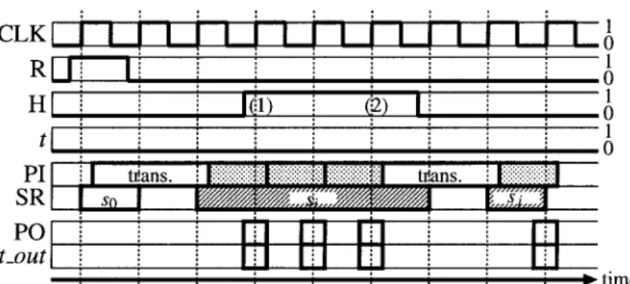
Step 1: Applying PPI value of a test pattern. First, we find a transition sequence from the reset state to the valid test state corresponding to the PPI value of the test pattern. Then, we set the valid test state to the SR (see Fig. 9) by applying the transition se- quence under the normal operation mode (the mode switching signal t = 0).
Notice that, if the combinational logic block contains a fault, we may not set the valid test state to the SR. However, the fault can be detected during the above step because the value loaded into the SR can be observed from t out.
Step 2: Applying PI value of a test pattern. We apply the PI value of the test pattern to the primary inputs of the sequential circuit (see Fig. 9).
Fig. 10. Applying valid test patterns using hold mode of state register.
For a valid test state, there may exist two or more valid test patterns which contain the valid test state. Therefore, the length of the test sequence can be re- duced if we apply the PI values of the test patterns one after another with holding the PPI value at the SR us- ing hold mode appended at the fifth step of the DFT process (see Fig. 10). Here, holding a value in the SR is called freezing the clock of the SR and the concept of freezing a clock is proposed by Abramovici et al. [15]. Moreover, a valid test state sjmay be reached from another valid test state si by transitions of the normal operation without reset. Therefore, we can reduce the length of a test sequence if we can set sj to the SR using the transitions without reset (see Fig. 10). Notice that, in this case, we have to hold the state si in the SR for one more cycle after applying all test patterns that contain the state sias (2) in Fig. 10. Hence a transition sequence which starts from the reset state and traverses
Fig. 11. Applying invalid test patterns.
all valid test states can set all PPI values to the SR. We call such a transition sequence a valid test state travers- ing sequence. Here, there always exists such a valid test state traversing sequence because any valid test state is reachable from the reset state and the reset state can be reached from any state using the reset signal. Let Lvtand Nvpbe the length of a valid test state traversing sequence and the number of valid test patterns, respec- tively. The length of a test sequence required to apply all valid test patterns is Lvt+Nvp.
We can obtain the shortest test sequence required to apply all valid test patterns, if we obtain the shortest valid test state traversing sequence. We can obtain the shortest valid test state traversing sequence by solv- ing the traveling salesman problem (TSP) [16] at a di- rected graph where nodes are all valid test states and the weight between nodes is the length of the shortest transition sequence between the two states. Although TSP is an NP-hard problem, we can obtain the shortest (or may be nearly shortest) valid test state traversing sequence using existing heuristic algorithms for TSP.
Notice that, time required to solve TSP is much shorter than the total test generation time of our method because the number of states of the FSM is generally much smaller than that of gates of the test generation model of the sequential circuit synthesized from the FSM.
Example 2. We consider the sequential circuit applied our DFT method of Example 1. The set of valid test states is {S0, S1, S2, S4, S9}. A valid test state travers- ing sequence required to apply the all invalid test pattern is S0→S1→S4→S0→S2→S5→S9. In the se- quence, if we reach a valid test state, we hold the state at the SR and apply the all test patterns which contains the valid test states from the primary inputs (Fig. 10).
5.2. Applying Invalid Test Patterns
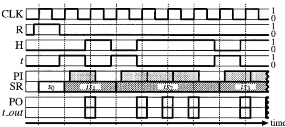
Each of invalid test patterns can be applied in the same way as valid test patterns using the ISG (invalid test state generator). In the rest of this paper, for simplicity, we assume that primary inputs are not used as inputs of the ISG. The transition modes are switched as shown in the timing chart of Fig. 11.
The length of the shortest invalid state transition se- quence (included applying reset signal at the begin- ning) is the number of invalid test states plus 1 because the ISG generates all invalid test states in turn. There- fore, letting Nisand Nipbe the numbers of invalid test states and invalid test patterns, respectively, the length of a test sequence required to apply all invalid test pat- terns is Nis+Nip+1. In the worst case, the length of the test sequence is only Nip×2 + 1.
Example 3. We consider the sequential circuit applied our DFT method of Example 1. The set of invalid test states is {IS1, IS2, IS3} and the invalid state transition sequence of the ISG is S0→IS1→IS2→IS3. From the reset state, we can generate the transition sequence if the mode switching signal t is one. The invalid test patterns can be applied by the same way as Example 2 (Fig. 11).
5.3. Testing of Extra Logic
Appended logic circuits in the DFT process are an ISG and an MUX added in front of the SR. Since the ISG is not used at the normal operation, we test the ISG only to confirm that the invalid test states are generated correctly. It is performed by observing state output signals t out at invalid test pattern application,
6.1. The Full-Scan DFT Method
Given a sequential circuit, the full-scan DFT method guarantees complete fault efficiency and can generate a test sequence with short test generation time because a test generation model of the sequential circuit is a combinational circuit. However, the method requires scan in/out operations for applying and observing test patterns, and thus it requires extremely long test ap- plication time. Letting AMUXand NFFbe the area of a MUX (two one bit inputs and one bit output) and the number of FFs, respectively, the area overhead of the method is NFF×AMUXbecause each FF of the SR is replaced with a scannable FF. Letting Npatbe the num- ber of test patterns, the test application time required to apply all test patterns and to observe the responses is Npat× (NFF+1) + NFF. Therefore, if the number of FFs of the SR is larger, the test application time is longer.
This method can be applied to large sequential cir- cuits. However, this method does not allow at-speed test application because the speed of scan sifting oper- ation is slower than the normal operation speed.
6.2. Patel’s Non-Scan DFT Method
Given a sequential circuit, Patel’s non-scan DFT me- thod appends an MUX to control the values of some FFs in the SR directly from primary inputs. The control- lable FFs are selected to cut feedback loops except self loops and to maximize controllability. The observabil- ity of the circuit is improved by inserting observation points which are connected to an XOR tree circuit with a primary output.
method can not guarantee complete fault efficiency and requires long test generation time generally because the test generation model is a sequential circuit. Moreover, the generated test sequence tends to become longer be- cause the sequence contains initialization sequences of FFs which are not controlled directly from primary in- puts. In this case, letting NPIbe the number of primary inputs, the area overhead is NPI×AMUX. Letting Lseq
be the length of obtained test sequence, the test appli- cation time required to apply all test patterns and to observe the responses is Lseq×2 + 1 cycles.
This method can be applied to large sequential cir- cuits and at-speed test application can be performed.
6.3. Our Method
Given a sequential circuit, our non-scan DFT method can guarantee complete fault efficiency. Test generation of our method for a controller consists of generating test patterns for the test generation model and obtain- ing a valid test state traversing sequence of the FSM. Test sequence for the controller is constructed from these test patterns using the valid test state traversing sequence. Those test patterns can be generated with short test generation time because the test generation model is a combinational circuit. Notice that, time re- quired to obtain the valid test state traversing sequence is negligible compared to the combinational test gen- eration time. Letting AISGbe the area of the ISG, the area overhead is NFF×AMUX+AISG. The ISG is a combinational logic which generates only invalid test states. In Section 6.4, we evaluate the area with expe- riments using FSM benchmarks. Letting Lvt and Nis
be the length of a valid test state traversing sequence and the number of invalid test states, respectively, the test application time required to apply all test patterns
and to observe the responses is Lvt+Nis+Npat+2 cycles.
In this method, at-speed test application can also be performed. However, this method is applicable only to sequential circuits which are designed as FSMs.
6.4. Experimental Results
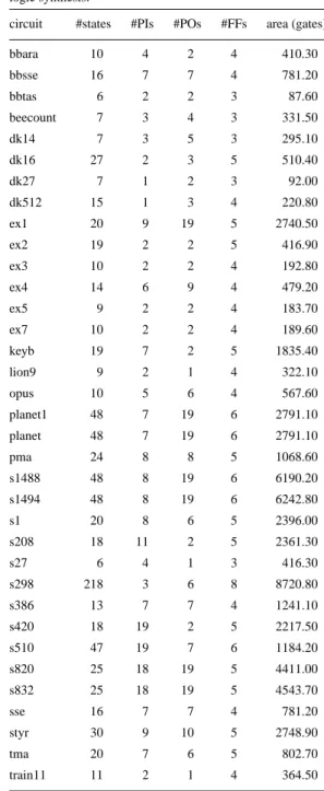
We show experimental results with MCNC’91 FSM benchmark set [17]. The benchmark characteristics and results of logic synthesis are shown in Table 1. In our ex- periment, we used a logic synthesis tool AutoLogic II (MentorGraphics) with sample libraries of Mentor- Graphics on S-4/20 model 712 (Fujitsu) workstation. Columns “circuit”, “#states”, “#PIs” and “#POs” de- note FSM name, the number of states, the number of primary inputs and the number of primary outputs of original FSMs, respectively. Columns “#FFs” and
“area” denote the number of FFs and circuit areas after synthesis, respectively. Here, areas are estimated using gate equivalent of the library cell area.
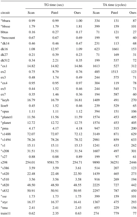
Table 2 shows test generation results of each method. We used a combinational/sequential test generation tool TestGen (Sunrise) on the workstation. Columns
“Scan”, “Patel” and “Ours” in column “TG time” de- note test generation time in seconds of the full-scan method, Patel’s method and our method, respectively. Test generation time of our method includes time for generating valid test state traversing sequences. In this experiments, in order to obtain a valid test state travers- ing sequence, we implemented a simple algorithm to solve the TSP. Column “TA time” denotes test appli- cation time in cycles.
Test generation time of the proposed method is al- most the same as that of the full-scan DFT method because test patterns are generated for the same com- binational test generation model and time to solve the TSP is short. In the column “circuit”, symbol “∗” de- notes that the number of primary inputs is larger than or equal to the number of FFs. In Patel’s method, the combinational test generation algorithm can also be ap- plied to these circuits. Thus Patel’s method guarantees complete fault efficiency for these circuit. Experimen- tal results show that fault efficiency of s298 is 99.55% and other circuits are 100% in Patel’s method. The full- scan method and our method guarantee complete fault efficiency for all circuits.
Test application time of the full-scan and Patel’s methods are calculated from the formulas mentioned
Table 1. FSM benchmark characteristics and areas after logic synthesis.
circuit #states #PIs #POs #FFs area (gates)
bbara 10 4 2 4 410.30
bbsse 16 7 7 4 781.20
bbtas 6 2 2 3 87.60
beecount 7 3 4 3 331.50
dk14 7 3 5 3 295.10
dk16 27 2 3 5 510.40
dk27 7 1 2 3 92.00
dk512 15 1 3 4 220.80
ex1 20 9 19 5 2740.50
ex2 19 2 2 5 416.90
ex3 10 2 2 4 192.80
ex4 14 6 9 4 479.20
ex5 9 2 2 4 183.70
ex7 10 2 2 4 189.60
keyb 19 7 2 5 1835.40
lion9 9 2 1 4 322.10
opus 10 5 6 4 567.60
planet1 48 7 19 6 2791.10
planet 48 7 19 6 2791.10
pma 24 8 8 5 1068.60
s1488 48 8 19 6 6190.20
s1494 48 8 19 6 6242.80
s1 20 8 6 5 2396.00
s208 18 11 2 5 2361.30
s27 6 4 1 3 416.30
s298 218 3 6 8 8720.80
s386 13 7 7 4 1241.10
s420 18 19 2 5 2217.50
s510 47 19 7 6 1184.20
s820 25 18 19 5 4411.00
s832 25 18 19 5 4543.70
sse 16 7 7 4 781.20
styr 30 9 10 5 2748.90
tma 20 7 6 5 802.70
train11 11 2 1 4 364.50
in Sections 6.1 and 6.2, respectively. Test application time of our method is calculated from the formula men- tioned in Section 6.3. In our method, for all circuits, the length of each test sequence is shorter than other two methods. Particularly, in s298, the ratio of our method to the full-scan method is one to four and of our method to Patel’s method is one to fifteen. If a more efficient
ex2 0.75 8.79 0.76 485 1513 123
ex3 0.48 1.74 0.49 244 575 71
∗ex4 0.95 0.95 0.97 304 119 78
ex5 0.44 1.52 0.46 244 545 71
ex7 0.35 1.46 0.36 194 587 60
∗keyb 16.79 16.79 16.81 1409 491 270
lion9 0.45 1.52 0.46 239 529 65
∗opus 1.11 1.11 1.12 394 151 106
∗planet1 11.56 11.56 11.59 1574 453 405
∗planet 12.72 12.72 12.75 1574 453 405
∗pma 4.17 4.17 4.18 947 315 200
∗s1488 72.07 72.07 72.12 3149 871 629
∗s1494 78.26 78.26 78.32 2981 859 633
∗s1 15.11 15.11 15.13 1241 433 262
∗s208 31.51 31.51 31.54 1607 497 301
∗s27 0.88 0.88 0.89 199 97 61
s298 254.01 9581.75 254.71 9890 36251 2446
∗s386 3.59 3.59 3.61 514 207 123
∗s420 22.48 22.48 22.50 1439 465 273
∗s510 3.56 3.56 3.58 916 269 194
∗s820 48.50 48.50 48.55 2225 727 442
∗s832 50.91 50.91 50.95 2297 787 450
∗sse 1.73 1.73 1.75 399 159 101
∗styr 16.37 16.37 16.41 1367 475 293
∗tma 2.41 2.41 2.43 653 229 156
train11 0.62 2.35 0.63 274 779 77
algorithm is shows used to solve the TSP, the test ap- plication time of our method may become shorter.
Table 3 area overheads of each method. Columns
“Scan”, “Patel” and “Ours” in column “#MUXes” de- note the number of MUXes of each method. The MUXes overhead of our method is equal to the full-scan method and is generally larger than Patel’s method.
Column “Our ISG area” denotes ISG area overhead in gate equivalent and percentage of the area for the corre- sponding controller. Here, each ISG was synthesized as Fig. 8. Although the order of generating valid test states affect the area of the ISG, in this experiments, we determined simply the order. Area overheads of circuits with “∗” in Table 2 are all zero because these
Table 3. Area overheads of each method.
#MUXes circuit Scan Patel Ours
Our ISG area (gates (ratio))
bbara 4 4 4 0 (0%)
bbsse 4 4 4 0 (0%)
bbtas 3 2 3 1.20 (1.36%)
beecount 3 3 3 0 (0%)
dk14 3 3 3 0 (0%)
dk16 5 2 5 39.30 (6.13%)
dk27 3 1 3 1.20 (1.30%)
dk512 4 1 4 7.00 (3.17%)
ex1 5 5 5 0 (0%)
ex2 5 2 5 34.70 (8.32%)
ex3 4 2 4 11.70 (6.06%)
ex4 4 4 4 0 (0%)
ex5 4 2 4 12.90 (7.02%)
ex7 4 2 4 14.10 (6.80%)
keyb 5 5 5 0 (0%)
lion9 4 2 4 1.20 (0.37%)
opus 4 4 4 0 (0%)
planet1 6 6 6 0 (0%)
planet 6 6 6 0 (0%)
pma 5 5 5 0 (0%)
s1488 6 6 6 0 (0%)
s1494 6 6 6 0 (0%)
s1 5 5 5 0 (0%)
s208 5 5 5 0 (0%)
s27 3 3 3 0 (0%)
s298 8 3 8 255.60 (2.16%)
s386 4 4 4 0 (0%)
s420 5 5 5 0 (0%)
s510 6 6 6 0 (0%)
s820 5 5 5 0 (0%)
s832 5 5 5 0 (0%)
sse 4 4 4 0 (0%)
styr 5 5 5 0 (0%)
tma 5 5 5 0 (0%)
train11 4 2 4 11.70 (3.20%)
circuits do not require ISGs. The average of ISG area overhead over the circuits requiring ISGs (excluding the circuits with “∗”) is only 3.5%. The smallest over- head is 0.37% and the largest is only 8.32%. The ISG area overhead can be more reduced as mentioned in Section 4.3.
Experimental results show that the proposed method guarantees complete fault efficiency and generates test patterns with short test generation time. Although some benchmarks require ISGs, the ISG area overhead is very small (the average of the area overhead is only 3.5%). Moreover, we also show that test application time of the proposed method is shorter than other two methods for all benchmarks.
7. Conclusion
Although the full-scan DFT method can achieve com- plete fault efficiency with short test generation time, it needs extremely long test application time. Moreover, it does not allow at-speed test application. Although Patel’s non-scan DFT method allows at-speed test ap- plication, it is not guaranteed to achieve complete fault efficiency with short test generation time.
In this paper, we proposed a new DFT method for controllers to achieve complete fault efficiency with short test generation time. The DFT method allows at- speed test application. We also proposed a test appli- cation method corresponding to the DFT method. Ex- perimental results show that the test application time of the proposed method is shorter than that of previous methods for all FSM benchmarks. The average area overhead of ISG is only 3.5% for FSM benchmarks which require ISGs to be appended.
Our future work is to design optimal ISG to mini- mize area overhead of ISG.
Acknowledgments
The authors would like to thanks Drs. Tomoo Inoue and Michiko Inoue of Nara Institute of Science and Technology for their valuable discussions. This work was supported in part by Semiconductor Technology Academic Research Center (STARC) under the Research Project.
Note
1. Fault efficiency is the ratio of the number of faults detected and proved redundant to the total number of faults.
References
1. H. Fujiwara, Logic Testing and Design for Testability, The MIT Press, 1985.
Theory and Applications, Vol. 1, pp. 221–228, 1990.
7. S. Kanjilal, S.T. Chakradhar, and V.D. Agrawal, “Test Function Embedding Algorithms with Application Interconnected Finite State Machines,” IEEE Transaction on Computer-Aided-Design, Vol. 14, No. 9, pp. 1115–1127, 1995.
8. S.T. Chakradhar, S. Kanjilal, and V.D. Agrawal, “Finite State Machine Synthesis with Fault Tolerant Test Function,” Journal of Electronic Testing: Theory and Applications, Vol. 4, pp. 57– 69, 1993.
9. I. Pomeranz and S.M. Reddy, “Design and Synthesis for Testa- bility of Synchronous Sequential Circuits Based on Strong- Connectivity,” Proc. of International Symposium on Fault- Tolerant Computing, 1993, pp. 492–501.
10. D. Xiang, S. Venkataraman, W.K. Fuchs, and J.H. Patel, “Par- tial Scan Design Based on State Information,” Proc. of Design Automation Conference, 1996, pp. 807–812.
11. D. Xiang and J.H. Patel, “A Global Algorithm for the Partial Scan Design Problem Using Circuit State Information,” Proc. of International Test Conference, 1996, pp. 548–557.
12. V. Boppana and W.K. Fuchs, “Partial Scan Design Based on State Transition Modeling,” Proc. of International Test Conference, 1996, pp. 538–547.
13. E.M. Sentovich et al., “SIS: A System for Sequential Circuit Synthesis,” Technical Report UCB/ERL-M92/41, University of California, Berkeley, 1992.
14. H. Fujiwara and A. Yamamoto, “Parity-Scan Design to Reduce the Cost of Test Application,” IEEE Transaction on Computer- Aided-Design, Vol. 12, No. 10, pp. 1604–1611, 1993. 15. M. Abramovici, K.B. Rajan, and D.T. Miller, “FREEZE!: A
New Approach for Testing Sequential Circuits,” Proc. of Design Automation Conference, 1992, pp. 22–25.
16. M.R. Garey and D.S. Johnson, Computer and Intractability, W.H. Freeman and Company, 1979.
17. S. Yang, “Logic Synthesis and Optimization Benchmarks User Guide,” Technical Report 1991-IWLS-UG-Saeyang, Microelec- tronics Center of North Carolina, 1991.
neering Science, Osaka University between 1990–1994. He is now an associate professor of Graduate School of Information Science, Nara Institute of Science and Technology (NAIST). He was also a visiting associate professor of Department of Computer Science, Cornell University between 1993–1994. His research interests in- clude digital systems design and test, distributed algorithms and parallel algorithms. He is a member of ACM, IEEE, EATCS, the Institute of Electronics, Information and Communication Engineers of Japan and the Information Processing Society of Japan.
Hideo Fujiwara received the B.E., M.E., and Ph.D. degrees in elec- tronic engineering from Osaka University, Osaka, Japan, in 1969, 1971, and 1974, respectively. He was with Osaka University from 1974 to 1985 and Meiji University from 1985 to 1993, and joined Nara Institute of Science and Technology in 1993. In 1981 he was a Visiting Research Assistant Professor at the University of Waterloo, and in 1984 he was a Visiting Associate Professor at McGill Uni- versity, Canada. Presently he is a Professor at the Graduate School of Information Science, Nara Institute of Science and Technology, Nara, Japan.
His research interests are logic design, digital systems design and test, VLSI CAD and fault tolerant computing, including high-level/ logic synthesis for testability, test synthesis, design for testability, built-in self-test, test pattern generation, parallel processing, and computational complexity. He is the author of Logic Testing and Design for Testability (MIT Press, 1985). He received the IECE Young Engineer Award in 1977, IEEE Computer Society Certificate of Appreciation Award in 1991, Okawa Prize for Publication in 1994, and IEEE Computer Society Meritorious Service Award in 1996. He is an advisory member of IEICE Trans. on Information and Systems and an editor of IEEE Trans. on Computers, J. Electronic Testing, J. Circuits, Systems and Computers, J. VLSI Design and others. Dr. Fujiwara is a fellow of the IEEE and a Golden Core member of the IEEE Computer Society as well as a member of the Institute of Elec- tronics, Information and Communication Engineers of Japan and the Information Processing Society of Japan.