Universal Test Complexity of Field-Programmable Gate Arrays
Tomoo Inoue
†, Hideo Fujiwara
†, Hiroyuki Michinishi
††, Tokumi Yokohira
††and Takuji Okamoto
†††Graduate School of Information Science ††Department of Information Technology Nara Institute of Science and Technology Faculty of Engineering, Okayama University
Takayama, Ikoma, Nara, 630-01 Japan Tsushima-naka, Okayama, 700 Japan
A bst rac t : A field-programmable gate array (FPGA) can implement arbitrary logic circuits in the field. In this paper, we consider universal t e s t such that when applied to an unprogrammed FPGA, it ensures that all the corresponding programmed logic circuits on the FPGA are fault-free. We focus on testing for look-up tables in FPGAs, and present two types of programming schemes; sequential loading and random access loading. Then we show test procedures for the FPGAs with these programming schemes and their test complexities. In order to make the test complexity for FPGAs independent of the array size of the FPGAs, we propose a programming scheme called b l o c k - s l i c e d loading, which makes FPGAs C - t e s t a b l e.
1. Introduction
Field-programmable gate arrays (FPGAs) are digital devices that can implement logic circuits required by users in the field [1,2]. Because of their short turnaround time, low manufacturing cost and programmability in the field, there has been an increasing interest in system prototyping and system reconfiguration using FPGAs. There are many different architectures of FPGAs driven by different programming technologies. One important class is the SRAM-based FPGAs (e.g. Xilinx [1-3]), also called the look-up table FPGAs, which can be reprogrammed any number of times. A novel feature of these FPGAs is that each basic block can implement any logic function that satisfies the I/O constraints of the basic block. The interconnections between the basic blocks consist of metal segments joined by program controlled pass transistors. In this paper, we shall consider look-up table FPGAs.
Testing for FPGAs, as well as conventional digital ICs, is one of the important problems. Several works on testing FPGAs have been reported [4,5]. Hermann and Hoffmann [4] presented fault models and test generation for one-time programmable FPGAs (e.g. Actel's [1,2]). Durate and Nicolaidis [5] reported a test methodology for cellular-based FPGAs (e.g. Algotronix's [1,2]). For reprogrammable FPGAs, two types of testing can be considered; one is testing for unprogrammed FPGAs, and the other is testing for programmed FPGAs. An unprogrammed FPGA can realize many different programmed FPGAs by loading different programs. Therefore, to test the unprogrammed FPGA, we might have to test all the programmed FPGAs obtained from the unprogrammed FPGA. However, it is too time-consuming to test such a large number of programmed FPGAs. In order to resolve this intractable problem, we
have to consider alternative approaches to testing for unprogrammed FPGAs.
In this paper, we shall introduce universal test such that when applied to a given unprogrammed FPGA, it ensures that all programmed FPGAs corresponding to the unprogrammed FPGA are fault-free. Here, we focus on testing for look-up tables in FPGAs. Testing for other components in an FPGA can be considered in the same way as testing for look-up tables. Then we shall present test complexity of FPGAs, where test complexity of an FPGA refers to the time required to test the FPGA. We shall present two types of programming schemes; sequential loadingand random access loading, and show that the test complexities of FPGAs with these programming schemes are O(Nnlog n) and O(Nn), respectively, where N is the array size of FPGAs or the number of configurable logic blocks, and n is the size of look-up tables or the number of configuration memory cells for each look-up table. The test complexities of these FPGAs depend on the array size N, and thus they might not be C-testable [6]. If we can make FPGAs C-testable, we can considerably reduce the test complexity. Therefore, we shall propose a new programming scheme, called block-sliced loading, which makes FPGAs C- testable. The test complexities of the proposed block-sliced FPGAs are O(nlog2n + log3n) and O(n + log n) for sequential loading and random access loading, respectively. 2. Architecture of F P G A s
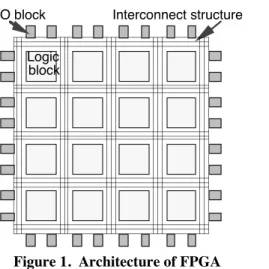
The architecture of field-programmable gate arrays (FPGAs) considered in this paper is illustrated in Fig. 1. An FPGA consists of an array of programmable logic blocks, programmable I/O blocks, and a programmable interconnect structure. Each logic block consists of a single look-up table (LUT). These blocks and interconnect structures are configured by static RAMs called configuration memory cells. This FPGA is referred to as a look-up table FPGA.
A look-up table implements combinational logic as a 2k
× 1 memory composed of configuration memory cells, where k is the number of input lines of the FPGA. When an input pattern is applied to a look-up table, the look-up table selects a configuration memory cell addressed by the input pattern, and the output of the cell provides the value of the function. A look-up table can implement any of 2n functions of its inputs, where n = 2k. When the FPGA is programmed, the memory is loaded with the bit pattern corresponding to the truth table of the function. Fig. 2(a) shows a block of a three-input LUT.
1995 IEEE Asian Test Symposium, pp.259-265, November 1995.
Figure 1. Architecture of FPGA I/O block Interconnect structure
Logic block
Figure 2. Configurable components (a) Look-up table
(b) Pass transistor (c) Multiplexer
Figure 3. Configurable logic block
A pass transistor controlled by a configuration memory cell, as shown in Fig. 2(b), configures a connection of wiring segments in an interconnect structure. The wire segments on each side of the transistor are connected or not, depending on the value in the memory cell. A multiplexer, as shown in Fig. 2(c), also controls a connection of wiring segments, and is a special-case one-directional routing structure. Multiplexers may be of any width, with more configuration memory cells for wider multiplexers. Fig. 3 shows the building blocks from Fig. 2 combined into a configurable logic block(CLB) with wiring. The CLB in Fig. 3 includes a single three-input LUT surrounded by wiring channels. Each wiring channel contains several segments. Segments have connections to the CLB and to each other through pass transistors and multiplexers.
A look-up table FPGA is programmed by loading a program composed of a bit sequence into its configuration memory cells. Each bit of the program is stored in the corresponding configuration memory cell, and consequently LUTs and interconnections are configured. Accordingly a logic function or a configuration is implemented on the FPGA. The FPGA must include circuitry to load a program. Here we consider two types of programming schemes as follows.
Sequential loading: When an FPGA is programmed, the program is shifted into the FPGA, and each bit of the program is stored in the corresponding configuration memory cell. This type of loading scheme is called sequential loading, and an FPGA with this type of loading is called a sequentially loadable FPGA (S L-FPGA). Whenever an SL-FPGA implements configurations, it loads all configuration memory cells.
Random access loading: Each configuration memory cell is directly addressable. When an FPGA is programmed, each bit is loaded by means of its address, and stored in the corresponding cell. This type of loading scheme is called random access loading, and an FPGA with this type of loading is called a random access loadable FPGA (R A L- FPGA). An RAL-FPGA can implement a configuration by loading only the bits which differ from those of the previous one.
3. Universal Test and Its C o m p l e x i t y 3.1 Universal Te s t
We can consider testing for FPGAs as two types of testing; one is testing for unprogrammed FPGAs, and the other is testing for programmed FPGAs. An FPGA implements different configurations or logic circuits by loading different programs. Therefore, in order to test the unprogrammed FPGA, we might have to test all the configurations implemented by the unprogrammed FPGAs. However, it is too time-consuming to test such a large number of configurations. To resolve this intractable problem, we introduce universal test such that when applied to a given unprogrammed FPGA, it ensures that all the corresponding configurations are fault-free.
3.2 Fault Model
The target of universal test is to detect faults that exist in an unprogrammed FPGA. An LUT is one of the important configurable components in look-up table FPGAs. Therefore, in the rest of paper we focus on testing for LUTs in FPGAs. Testing for other components in an FPGA can be considered in the same way as testing for LUTs. A k- input LUT consists of 2k configuration memory cells, and each memory cell has its own address. When an input pattern is applied to the LUT from its k input lines, the LUT decodes the input pattern, and reads out the memory cell corresponding to the input pattern. Thus, LUTs can be considered as random access memories (RAMs). However, since the decoder for writing is different from the decoder for reading, we can not apply conventional methods for testing of RAMs [7,8] to such LUTs. Hence, we have to consider an alternative method for testing of LUTs. The fault models assumed in this paper are as follows.
Stuck-at faults of memory cells: One or more logic values in the memory cells cannot be changed for any configuration. Such faults are called stuck-at faults (SAFs). When an input pattern corresponding to an SAF memory cell, the output value for the input pattern is either 0 or 1, irrespective of configurations.
Let k be the number of input lines of an LUT. Let n = 2k be the number of memory cells of the LUT. Let A =
{a0, a1, ..., an–1} denote a set of input patterns for the LUT, i.e., a set of addresses of memory cells of the LUT. Let M
= {m0, m1, ..., mn–1} denote a set of memory cells in the LUT. The fault-free decoding function of an LUT can be modeled as a mapping f from A to M such that f(ai) = mi for all i. As faulty decoding functions, we can consider the following three cases.
Incorrect access faults (IAFs): For some ai, f(ai) = mj ≠ mi due to a fault. That is, whenever memory cell mi is to be accessed by input pattern ai, different memory cell mj is accessed.
Non-access faults (NAFs): For some ai, f(ai) is empty due to a fault. That is, whenever memory cell ai is to be accessed, no memory cell is accessed. Here, the output value for the input pattern ai depends on the previous output value of the LUT.
Multiple access faults (MAFs): For some ai, f(ai) is neither singleton nor empty due to a fault. That is, whenever memory cell mi is accessed, more than one memory cell are accessed. Here, the output value is formed either by the bit- wise OR or AND function (depending on the technology) over the memory cells of the set f(ai).
Hereafter, we consider universal test for these faults of LUTs under single fault assumption.
3.3 Test C o m p l e x i t y
Universal test is performed by repeating implementation of a configuration and application of an input sequence to the configuration alternately. Hence, a test procedure for the universal testing is represented as a sequence of pairs of a configuration and its input sequence. Let Ci be the i-th configuration in a test procedure TP, and Let S i be the input sequence for the i-th configuration of the test procedure TP. Then, we can express a test procedure as
TP= C1, S1, C2, S2 , ..., Cnc, Snc (1) where nc is the number of pairs of a configuration and its input sequence in test procedure TP. Let c(i) be the number of configuration memory cells that are loaded to implement the i-th configuration, i.e., the bit size of a program for the i-th configuration. For an SL-FPGA, the size of each program is constant, i.e.,
c i = Nm (2)
where Nm is the total number of configuration memory cells in the FPGA. For a RAL-FPGA, c(i) becomes the number of different bits between consecutive configurations Ci–1 and Ci. Note that c(1) = Nm. Let ns(i) be the length of input sequence S i for the i-th configuration Ci.
The time required to test an FPGA by a test procedure TPcan be expressed as
T TP =
Σ
tcc i + tsnsii= 1 nc
(3) where tc is the time required to load one bit of a program into a configuration memory cell in the FPGA, and ts is the clock cycle time of a configuration implemented in the FPGA. By denoting
Ns=
Σ
ns ii= 1 nc
, (4)
Eq. (3) can be expressed as T TP =
Σ
tcc ii= 1 nc
+ tsNs. (5) From Eqs. (2) and (5), the test complexity of test procedure TPfor SL-FPGAs or the time required to test SL-FPGAs by test procedure TP can be expressed as
TSL TP = tcncNm+ tsNs. (6) For RAL-FPGAs, we can let
Nc=
Σ
c ii= 1 nc
. (7)
By substituting this equation for Eq. (5), we have the test complexity of test procedure TP for RAL-FPGAs as follows.
TRAL TP = tcNc+ tsNs (8)
4. Test procedure and Test C o m p l e x i t y 4.1 Testing for S L - F P G A s
First, we consider testing for a single LUT of SL- FPGAs. Testing for an LUT can be considered to ensure that each memory cell in the LUT is read out correctly by applying the corresponding input pattern. Here we present a test procedure called TP-SL for a single LUT of an SL- FPGA. Let k be the number of input lines of an LUT. Let n= 2k be the number of memory cells in the LUT or the size of the LUT. Let ai be an input pattern that access the corresponding memory cell mi. To simplify the discussion, unless otherwise noted, from now we assume that input pattern ai denotes a binary code of i for all i without loss of generality. Let b(i, j) be the i-th bit of the binary code of j, e.g., b(2, 4) = 1 since (4)10 = (100)2. Then, test procedure TP-SLis as follows:
Test Procedure T P - S L: Step 1: for (i := 1 to k) {
Step 1.1: for (j := 0 to n – 1) { # the i-th configuration Load b(k – i, j) into memory cell mj }
Step 1.2: for (j := 0 to n – 1) { # read all memory cells Read mj with input pattern aj
} }
Step 2: for (i := k + 1 to 2k) {
Step 2.1: for (j := 0 to n – 1) { # the i-th configuration Load the complement of b(2k – i, j)
into memory cell mj }
Step 2.2: for (j := n – 1 to 0) {
# read all memory cells in the reverse order Read mj with input pattern aj
} }
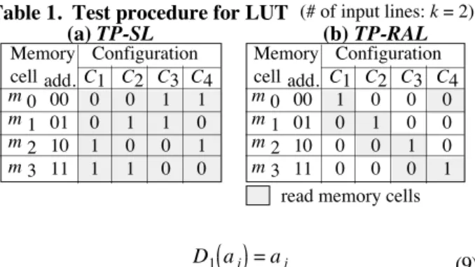
Table 1(a) shows an example of test procedure TP-SL for a two-input LUT. As shown in this table, a collection of each memory cell mj at Step 1 denotes its address aj, and a collection of each memory cell mj at Step 2 denotes the bit- wise complement of its address aj. Let D1(aj) be a sequence of the output bits when reading memory cell mj at Step 1 of TP-SL. This sequence D1(aj) denotes the address of memory cell mj, i.e.,
Table 1. Test procedure for LUT (# of input lines: k = 2)
read memory cells C1 C2 C3 C4
0 0 1 1
0 1 0 1
1 0 1 0 1 1 0 0 Configuration Memory
cell m 0m 1 m 2 m 3
00 01 10 11 add.
1 0 0 0
0 1 0 0
0 0 0 1 0 0 1 0 C1 C2 C3 C4
Configuration Memory
cell m 0m 1 m 2 m 3
00 01 10 11 add.
(a) TP-SL (b) TP-RAL
D1 aj = aj (9)
for all j. Let D2(aj) be a sequence of the output bits when reading memory cell mj at Step 2 of TP-SL. This sequence D2(aj) denotes the bit-wise complement of the address of memory cell mj, i.e.,
D2 aj = aj= D1 aj (10) for all j. Then, we have the following lemmas.
Lemma 1 : TP-SL can detect any SAF.
Proof: If a memory cell mj is stuck at 0 (1), mj = 0 (1) for any configuration. Hence,
D1aj = D2 aj = 00...0 (11...1) . (11) This equation is inconsistent with Eq. (10). Hence TP-SL
can detect any SAF. □
Lemma 2 : TP-SL can detect any IAF.
Proof: If an input pattern aj selects a memory cell mi instead of mj,
D1 aj = ai D2 aj = ai
(12) (13) These equations are inconsistent with Eqs. (9) and (10), respectively. Hence TP-SL can detect any IAF. □ Lemma 3 : TP-SL can detect any NAF.
Proof: When i = k at Step 1, memory cells m0, m1, ..., mn–2 and mn–1 are loaded with 0,1,...,0 and 1, respectively. Each memory cell loaded with 0 (1) is read after reading out the opposite value 1 (0) except m0. Similarly, memory cell m0 loaded with 1 is read after reading 0 when i = 2k. If an input pattern aj selects no memory cell, then the output value keeps the previous one, and does not alternate with 0 and 1. Hence TP-SL can detect any NAF. □ Lemma 4 : TP-SL can detect any MAF.
Proof: If an input pattern aj selects not only memory cell mj but also another memory cell mi, then
D1 aj = aj* ai D2 aj = aj* ai
(14) (15) where * denotes the bit-wise function depending on technology. Hence,
D1aj ≠ D2aj (16)
This equation is inconsistent with Eq. (10). Hence TP-SL
can detect any MAF. □
From Lemmas 1 to 4, we can see that test procedure TP- S Lcan detect any faults of an LUT. Therefore, we have the following theorem.
Theorem 1 : Test procedure TP-SL can detect any fault in an LUT.
Next, let us consider the test complexity of test procedure TP-SL. Test procedure TP-SL consists of Step1 and Step2, and k configurations are implemented in each step. Hence, the total number of configurations is
nc = 2k = 2 log n . (17) Moreover, each memory cell is read out once for each configuration. Hence,
ns i = n for 1 ≤ i ≤ nc. (18) Therefore, from Eq. (6) the time required to test one LUT of an SL-FPGA is
TSL TP–SL = 2Nmlog n tc+ 2n log n ts
= O N m+ n log n . (19) Let N be the array size of the FPGA, i.e., the number of LUTs in the FPGA. Since the total number of configuration memory cells, Nm, depends on the array size Nand on the total number of configuration memory cells n, Eq. (19) can be also expressed as
TSLTP–SL = O Nn log n . (20) Hence, we have the following theorem.
Theorem 2 : The test complexity of test procedure TP-SL for a single LUT of an SL-FPGA is O(Nn log n), where N is the array size of the FPGA and n is the size of the LUT.
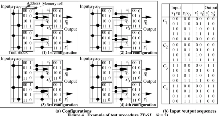
Next we consider testing for all LUTs in an SL-FPGA. If we can use any number of primary I/Os, we can test all LUTs in an FPGA simultaneously. However, since an FPGA has a restricted number of I/O blocks, we cannot apply the same test patterns to all LUTs directly and simultaneously. We have to consider another method of testing for all LUTs under such a constraint of the limited number of I/O blocks. In test procedure TP-SL, as shown by Eqs. (9) and (10), output sequences of an LUT become addresses of its memory cells. Hence, we can use the output sequences of an LUT as input patterns for another LUT. If we consider k LUTs to be a block which has k input lines and k output lines, all the 2k patterns can be extracted from the output of the block. Therefore, we can test any number of LUTs concurrently with test procedure TP-SL by cascading such blocks by applying all the 2k input patterns to the block. These blocks are called test blocks. Fig. 4 shows an example in case of k = 2. Fig. 4(a) illustrates 4 (=2k) configurations for all LUTs in an SL-FPGA. Here, two LUTs are combined into a single test block, shown outlined, and test blocks are cascaded from left to right. In this cascade, connections between blocks are configured to generate the input/output sequences of Fig. 4(b). The first leftmost test block can be tested since all the input sequences of test procedure TP-SL are included in the first column of this table. Here, the output patterns of the first test block (i.e., the second column) are transferred to the inputs of the next test block (i.e., the third column). Hence, all patterns can be applied to the second test block for each configuration. In configurations C1and C2, input sequences for the second test block coincide with input sequences for
the first block. However, in configurations C3 and C4, input sequences for the second test block are the reverse of those for the first test block. Therefore, all faults except NAFs for the first memory cells (m0) in the second test block can be detected. To detect the NAFs, the last input/output pattern in configuration C1 is added. In this way, all test blocks in the cascade can be tested by the input/output sequences of Fig. 4(b). This test procedure can be easily extended to an arbitrary size k. Hence, we have the following theorem.
Theorem 3 : There exists a test procedure for SL-FPGAs such that the test complexity is O(Nn log n), where N is the array size of the FPGAs and n is the size of LUTs. 4.2 Testing for RAL-FPGAs
Next we present a test procedure for a single LUT of a RAL-FPGA, called TP-RAL. In the following test procedure, we assume that FPGAs behave the bit-wise AND function toward MAFs. For FPGAs that behave the bit- wise OR function, we can get the same test procedure by complementing load values in test procedure TP-RAL. Test Procedure T P - R A L :
for (i := 1 to n) { # the i-th configuration if (i = 1) { # Initial configuration
for (j := 1 to n – 1) {
Step 1.1: Load 0 into memory cell mj }
} else {
Step 1.2: Load 0 into memory cell mp }
Step 2: j:= i – 1
Load 1 into memory cell mj
Step 3: Read memory cell mj with input pattern aj if (i < n) {
Step 4.1: p:= j + 1 } else { Step 4.2: p:= 0
}
Step 4.3: Read memory cell mp with input pattern ap }
Table 1(b) shows an example of test procedure TP-RAL for a two-input LUT. As shown in this table, for each configuration, only one memory cell is programmed with 1, and all other memory cells are programmed with 0.
Let d1(j) be the output value obtained by reading mj at Step 3. Let d2(j) be the output value obtained by reading mj at Step 4.3. If an LUT is fault-free, then
d1 i = 1 d2 i = 0
(21) (22) for 0 ≤ j ≤ n – 1. Then, we show the following lemmas. Lemma 5 : TP-RAL can detect any SAF.
Proof: If a memory cell mj is stuck at 0 (1), then d1(j) = d2(j) = 0 (1). This is inconsistent with Eqs. (21) and (22).
Hence, TP-RAL can detect any SAF. □
Lemma 6 : TP-RAL can detect any IAF.
Proof: As mentioned above, all memory cells except mi–1 is programmed with 0 on the i-the configuration for all i. Hence, if an input pattern aj selects a memory cell ml
instead of mj, then d1(j) = 0 at Step 3. This is inconsistent with Eq. (21). Hence, TP-RAL can detect any IAF. □ Lemma 7 : TP-RAL can detect any NAF.
Proof: For all i, 0 is read out with input pattern ap at Step 4.3 after 1 is read out at Step 3. If an input pattern ap selects no memory cell, then d2(p) = 1 instead of 0, because the output keeps the previous value, 1. This is inconsistent with Eq. (22). Hence, TP-RAL can detect any NAF. □ Lemma 8 : TP-RAL can detect any MAF.
Proof: As mentioned above, all memory cells except mi–1 is programmed with 0 on the i-th configuration for all i. Hence, for any pair of memory cells mαand mβsuch that α
≠β,
mi∧ mj= 0 (23)
If an input pattern aj selects two memory cells, mαand mβ, then d1(j) = 0. This is inconsistent with Eq. (21). Hence,
TP-RALcan detect any NAF. □
From Lemmas 5 to 8, we have the following theorem. Theorem 4 : Test procedure TP-RAL can detect any fault in an LUT.
Next, let us consider the test complexity of test procedure TP-RAL for a single LUT of a RAL-FPGA. In test procedure TP-RAL, n configurations are implemented, i.e.,
nc = n . (24)
For i = 1, all the memory cells in the LUT are loaded. Hence,
c(1) = n . (25)
For 2 ≤ i ≤ n, only two memory cells are loaded at Steps 2.1 and 2.2. Hence,
c(i) = 2 for 2 ≤ i ≤ n. (26) Moreover, only two memory cells are read out at Steps 3 and 4. Therefore,
ns(i) = 2 for 1 ≤ i ≤ n. (27) From these equations and Eq. (8), the time required to test one LUT in an RAL-FPGA is given by
TRALTP–RAL = n + 2 n–1 tc+ 2nts
= 3n–2 t c+ 2nts. (28) Accordingly, we have the following theorem.
Theorem 5: The test complexity of test procedure TP- R A Lfor a single LUT of a RAL-FPGA is O(n), where n is the number of memory cells of the LUT , i.e., the size of the LUT.
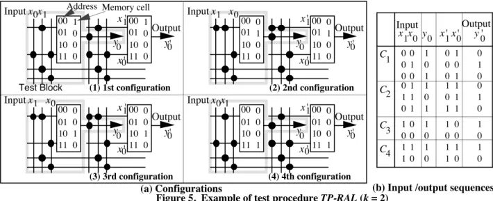
Next we consider testing for all LUTs in an RAL-FPGA. In the same way as SL-FPGAs, we consider a cascade of test blocks to test all the test blocks simultaneously. We can generate input/output sequences and configurations so that output sequences of each test block can be used as input sequences of the next test block. In order to illustrate this, we show an example in case of k = 2 in Fig. 5. Fig. 5(a) illustrates 4 (= 2k) configurations for all LUTs in a RAL- FPGA. Here, one LUT is a single test block, shown outlined, and test blocks are cascaded from left to right. In this cascade, connections between test blocks are configured to generate the input/output sequences of Fig. 5(b). The first and the third columns of this table show the input
Figure 4. Example of test procedure TP-SL (k = 2)(b) Input /output sequences (a) Configurations
x0
x1 y
y1 0 y
1' y 0' x1' x0' 0
0 1 1 0 0 1 0 1 0
0 0 1 1 0 0 1 0 1 0
0 0 1 1 0 0 1 0 1 0
0 0 1 1 0 0 1 0 1 0 C1
Input Output
0 0 1 1 0 1 0 1
0 0 1 1
0 1 0 1
0 0 1 1 0 1 0 1
0 0 1 1
0 1 0 1 C2
1 1 0 0 1 0 1 0
0 0 1 1 0 1 0 1
0 0 1 1 0 1 0 1
1 1 0 0 1 0 1 0 C3
1 1 0 0 1 0 1 0
0 0 1 1
0 1 0 1
0 0 1 1 0 1 0 1
1 0 1 0
1 1 0 0 C4
(1) 1st configuration 0
0 1 1 0 1 0 1
0 0 1 1 0 1 0 1 Input
Output y0
y1' 00
01 10 11 00 01 10 11
00 01 10 11 x0
x1
00 01 10 11 y '
0
y1 x0'
x1' Address Memory cell
Test Block
0 1 0 1 0 0 1 1 Input
Output y0
y1' 00
01 10 11 00 01 10 11
00 01 10 11 x0
x1
00 01 10 11 y '
0
y1 x0' x1'
(2) 2nd configuration 0
1 0 1 0 0 1 1
1 1 0 0 1 0 1 0 Input
Output y0
y1' 00
01 10 11 00 01 10 11
00 01 10 11 x0
x1
00 01 10 11 y0 '
y1 x0'
x1'
(3) 3rd configuration 1
1 0 0 1 0 1 0
1 0 1 0 1 1 0 0 Input
Output y0
y1' 00
01 10 11 00 01 10 11
00 01 10 11 x0
x1
00 01 10 11 y0 '
y1 x0' x1'
(4) 4th configuration 1 0 1 0 1 1 0 0
sequences of the next test block. In order to illustrate this, we show an example in case of k = 2 in Fig. 5. Fig. 5(a) illustrates 4 (= 2k) configurations for all LUTs in a RAL- FPGA. Here, one LUT is a single test block, shown outlined, and test blocks are cascaded from left to right. In this cascade, connections between test blocks are configured to generate the input/output sequences of Fig. 5(b). The first and the third columns of this table show the input sequences for the leftmost and the next test blocks, respectively. From test procedure TP-RAL, we can see that the input sequences necessary to test each test block are (00,01), (01,11), (10,00) and (11,10) for C1, C2, C3 and C4, respectively. These input sequences are all included in the first and the third columns of the table. Therefore, the leftmost and the next test blocks are tested by the input/output sequences. In this way, all test blocks in the cascade can be tested by the input/output sequences of Fig. 5(b). This test procedure can be easily extended to an arbitrary size k. Hence, we have the following theorem. Theorem 6 : There exists a test procedure for a RAL- FPGA such that the test complexity is O(Nn), where N is the array size of the RAL-FPGA, and n is the size of each LUT of the RAL-FPGA.
Proof: The number of configurations in test procedure TP- R A Lis expressed as:
nc = n. (29)
Since all the memory cells in the FPGA are loaded for the first configuration C1,
c(1) = Nm . (30)
For each configuration Ci (2 ≤ i ≤ n), two memory cells of each LUT are loaded with 0 and 1. On the other hand, one connection between the primary inputs and one of input lines of each test block is changed for each configuration.
Moreover, the number of test blocks is equal to the array size of the FPGA, N, since each test block includes a single LUT. Hence,
c(i) = 4N for 2 ≤ i ≤ n . (31) Three input patterns and two input patterns are applied for 1
≤ i ≤n/2 and for n/2+1 ≤ i ≤ n, respecitively, i.e.,
nsi = 3 for 1 ≤ i ≤n2, and
ns i = 2 for n
2+ 1 ≤ i ≤ n . (32) Thus, the time required to test RAL-FPGAs by test procedure TP-RAL can be expressed as
TRALTP–RAL = Nm+ 4N n–1 tc+ 5
2nts. (33) Since the total number of configuration memory cells Nm depends on the number of LUTs in a FPGA and on the number of memory cells of each LUT, the test complexity of test procedure TP-RAL for RAL-FPGAs can be expressed as
TRALTP–RAL = O Nn . □(34)
5. C - Testable F P G A s
Since an FPGA consists of an array of logic blocks, it can be considered to be one of iterative systems. 'C-testable' [6] is a term which expresses an important class of testable iterative systems.
Definition ( C - t e s t a b l e ) : Suppose an iterative array consisting of N logic cells. If the iterative array can be tested with a number of test patterns that does not depend on N, then the iterative array is said to be C-testable.
In each of test procedures TP-SL and TP-RAL, if we regard each test block as a logic cell, each configuration can be considered to be an iterative system. Moreover, the length of input sequences applied to each configuration is
Figure 5. Example of test procedure TP-RAL (k = 2)
(b) Input /output sequences (a) Configurations
x0
x1 y0 x1' x0' y0'
0 1 0 0 0 0
1 0 1
0 0 0
1 0 1
0 1 0 C1
Input Output
1 1 1 0 1 0
1 0 1
1 0 1
1 1 1
0 1 0 C2
0 0 1 0
1 0
0 0 1 0
1 3 0
C
1 0 1 1
1 0
1 1
1 0
1 4 0
C (1) 1st configuration
1 0 0 0
(2) 2nd configuration
(3) 3rd configuration (4) 4th configuration
1 0 0 0 Input
Output y0' y0
x0' x1' 00
01 10 11
00 01 10 11 x0x1
Test Block
Address Memory cell
0 1 0 0
0 1 0 0 Input
Output y0' y0
x0' x1' 00
01 10 11
00 01 10 11 x0
x1
0 0 1 0
0 0 1 0 Input
Output y0' y0
x0' x1' 00
01 10 11
00 01 10 11 x0
x1
0 0 0 1
0 0 0 1 Input
Output y0' y0
x0' x1' 00
01 10 11
00 01 10 11 x0x1
independent of the array size of FPGAs. On the other hand, from Eqs. (19) and (34), we can see that the time required to load programs for testing FPGAs depends on the array size of the FPGAs. Therefore, if an FPGA can load the same program into each test block simultaneously, the time required to load programs will be independent of the array size. Such type of programming schemes is called block- sliced loading, and SL-FPGAs and RAL-FPGAs with block- sliced loading are referred to as BSSL-FPGAs and BSRAL- FPGAs, respectively.
Let tb be the time required to load the same bit into the corresponding configuration memory cell of each test block. Let Nb be the size of each test block, i.e., the number of LUTs in each test block. Then, we have the following theorems.
Theorem 7 : BSSL-FPGAs are C-testable.
Proof: Each LUT is composed of n memory cells, k = log n input lines and one output line, and each test block consists of k = log n LUTs. Hence, the time required to test a BSSL- FPGA is given by
TBSSLTP–SL = Nb 2log n n+log n + 1 tb+ nts
= 2 log 3n+ n + 1 log2n tb+ 2n log n ts
= O n log 2n+ log3n . □(35) Theorem 8 : BSRAL-FPGAs are C-testable.
Proof: Since each test block consists of a single LUT, Nb
= 1. Each test block has k input lines and one output line, and the input/output lines are connected with k + 1 wiring segments. In the same way as Eq. (33), the time required to test BSRAL-FPGAs can be expressed as
TBSRALTP–RAL = n +2 log n + 1 + 4 n–1 tb+ 5 2nts
= O n + log n . □(36) From these Eqs. (35) and (36), we can see that the test complexity of BSRAL-FPGAs is lower than that of BSSL- FPGAs.
6. C o n c l u s i o n
In this paper, we considered universal test such that when applied to an unprogrammed FPGA, it ensures that all the corresponding programmed logic circuits on the FPGA are fault-free. We presented two types of programming schemes; sequential loading and random access loading, and showed test procedures for the FPGAs with these programming schemes and their test complexities. In order to make the test complexity for FPGAs independent of the array size of the FPGAs, we proposed a programming scheme called block-sliced loading, which makes FPGAs C-testable.
In this paper, we focused on testing for look-up tables in FPGAs. However, testing for other components, e.g. I/O blocks and interconnect structures, are also important. These components can be tested in the same way as testing for look-up tables. We will report in the near future on the testing for these components as well as the whole of FPGAs.
R e f e r e n c e s
[1] S.D. Brown, R.J. Francis, J. Rose, S.G. Vranesic, Field- Programmable Gate Arrays, Kluwer Academic Publishers, 1992.
[2] S.M. Trimberger (ed.), Field-Programmable Gate Array Technology, Kluwer Academic Publishers, 1994.
[3] The Programmable Logic Data B o o k, Xilinx, 1994.
[4] M. Hermann and W. Hoffmann, "Fault modeling and test generation for FPGAs," in R.W. Hartenstein and M.Z. Servít (eds.), Lecture Notes in Computer Science, Field Programmable Logic, Springer-Verlag, pp.1-10, 1994. [5] R.O. Durate and M. Nicolaidis, "A test methodology applied
to cellular logic programmable gate arrays," in R.W. Hartenstein and M.Z. Servít (eds.), Lecture Notes in Computer Science, Field Programmable Logic, Springer-Verlag, pp.11- 22, 1994.
[6] A.D. Friendman, "Easily testable iterative systems," IEEE Trans. on Comput. Vol. C-22, No. 12, pp.1061-1064, 1973. [7] M.S. Abadir and H.K. Reghbati, "Functional testing of
semiconductor random access memories," ACM Computing Surveys, Vol.15, No.3, pp.175-198, 1983.
[8] A. Tuszynski, "Memory testing," in T.W. Williams (ed.), VLSI Testing, Elsevier Science Publishers, pp.161-228, 1986.