[Date of Issue] December 2009 (Ver. D:July 2016)
[Relevant Models] A1NCPU, A2NCPU, A2NCPU-S1, A3NCPU, A2ACPU, A2ACPU-S1,
A3ACPU, A2UCPU, A2UCPU-S1, A3UCPU, A4UCPU, Q2ACPU,
Q2ACPU-S1, Q3ACPU, Q4ACPU, Q00UJCPU, Q00UCPU, Q01UCPU,
Q02UCPU, Q03UDCPU, Q03UDVCPU, Q03UDECPU, Q04UDHCPU,
Q04UDVCPU, Q04UDEHCPU, Q06UDHCPU, Q06UDVCPU,
Q06UDEHCPU, Q10UDHCPU, Q10UDEHCPU, Q13UDHCPU,
Q13UDVCPU, Q13UDEHCPU, Q20UDHCPU, Q20UDEHCPU,
Q26UDHCPU, Q26UDVCPU, Q26UDEHCPU
Thank you for your continued support of Mitsubishi programmable controllers.
This technical bulletin describes precautions for replacing an A/QnA (large type) series CPU with a Universal
model QCPU.
Note that the reference manuals or the references described in this bulletin are information as of July 2016.
Contents
GENERIC TERMS ... 2
1. Introduction ... 3
2.
Precautions for system configuration ... 4
2.1 Connection of the QA extension base unit ··· 4
2.2 Use of the Q series large type base unit ··· 9
2.3 GOT connection ··· 10
3. Utilizing
programs
... 11
3.1 Sequence instructions requiring a review before replacing the ACPU ··· 11
3.1.1 Replacement example of the PR instruction ··· 12
3.1.2 Replacement example of the KEY instruction ··· 16
3.2 Sequence instructions requiring a review before replacing the QnACPU ··· 19
3.2.1 Replacement example of the IX and IXEND instructions ··· 20
3.2.2 Replacement example of the IXDEV and IXSET instructions ··· 22
3.2.3 Replacement example of the PR instruction ··· 24
3.2.4 Replacement example of the CHKST and CHK instructions··· 28
3.2.5 Replacement example of the KEY instruction ··· 31
3.3 SFC (MELSAP-II/MELSAP3) ··· 34
3.3.1 Functions requiring a review before replacing the ACPU with SFC (MELSAP-II) ··· 34
3.3.2 Functions and instructions requiring a review before replacing the QnACPU with SFC (MELSAP3) ···· 35
4.
Precautions for the performance and specifications of the CPU modules... 37
4.1 Precautions for performance and specifications when the ACPU is replaced··· 37
4.2 Precautions for performance and specifications when the QnACPU is replaced ··· 39
4.3 Device latch function ··· 42
GENERIC TERMS
Generic term Description
ACPU (including CPU with link function) A generic term for A1NCPU, A2NCPU, A2NCPU-S1, A3NCPU, A2ACPU, A2ACPU-S1, A3ACPU, A2UCPU, A2UCPU-S1, A3UCPU, and A4UCPU
QnACPU A generic term for Q2ACPU, Q2ACPU-S1, Q3ACPU, and Q4ACPU A/QnA (large type) series CPU (including
CPU with link function)
A generic term for A1NCPU, A2NCPU, A2NCPU-S1, A3NCPU, A2ACPU, A2ACPU-S1, A3ACPU, A2UCPU, A2UCPU-S1, A3UCPU, A4UCPU, Q2ACPU, Q2ACPU-S1, Q3ACPU, and Q4ACPU
Universal model QCPU A generic term for Q00UJCPU, Q00UCPU, Q01UCPU, Q02UCPU, Q03UDCPU,
Q03UDVCPU, Q03UDECPU, Q04UDHCPU, Q04UDVCPU, Q04UDEHCPU, Q06UDHCPU, Q06UDVCPU, Q06UDEHCPU, Q10UDHCPU, Q10UDEHCPU, Q13UDHCPU,
Q13UDVCPU, Q13UDEHCPU, Q20UDHCPU, Q20UDEHCPU, Q26UDHCPU, Q26UDVCPU, and Q26UDEHCPU
1. Introduction
When replacing an A/QnA (large type) series CPU with a Universal model QCPU, please read this technical
bulletin with the following handbooks and materials. (Among replacement to the Universal model QCPU, this
bulletin describes contents that differ from those described in the following handbooks and materials.)
For contents not described in this bulletin, refer to the following handbooks.
Note that the Q00UJCPU, Q00UCPU, and Q01UCPU partly differ in specifications such as the number of I/O
points and the number of device points, and functions such as available instructions.
When the Q00UJCPU, Q00UCPU, or Q01UCPU replaces the existing CPU module, refer to the related
manuals to see if the CPU module after replacement meets the specifications and the functions of the existing
system.
(Handbook for transition (released))
Transition from MELSEC-A/QnA (Large Type) Series to Q Series Handbook
(Fundamentals) L-08043ENG
(Intelligent Function Modules) L-08046ENG
(Network Modules) L-08048ENG
(Communications) L-08050ENG
Transition from MELSEC-A0J2H Series to Q Series Handbook L-08060ENG Transition from MELSECNET/MINI-S3, A2C(I/O) to CC-Link Handbook L-08061ENG Transition from MELSEC-I/O LINK to CC-Link/LT Handbook L-08062ENG Transition from MELSEC-A/QnA Large Type Series to AnS/Q2AS Small Type Series Handbook L-08064ENG Transition of CPUs in MELSEC Redundant System Handbook (Transition from Q4ARCPU to QnPRHCPU) L-08117ENG
(Renewal catalogue)
MELSEC-A/QnA Series Transition Guide L-08077E
(Renewal examples)
2. Precautions for system configuration
This chapter describes precautions for system configuration when the Universal model QCPU replaces the
existing CPU module.
2.1 Connection of the QA extension base unit
To connect the QA extension base unit for using the A/QnA (large type) series modules, the Universal model
QCPU whose serial number (first five digits) is "13102" or later must be used.
When the Universal model QCPU whose serial number is "13101" or earlier is used, the QA extension base
unit cannot be connected. This means that the A/QnA (large type) series modules cannot be used in the
system. All modules need to be replaced with Q series modules.
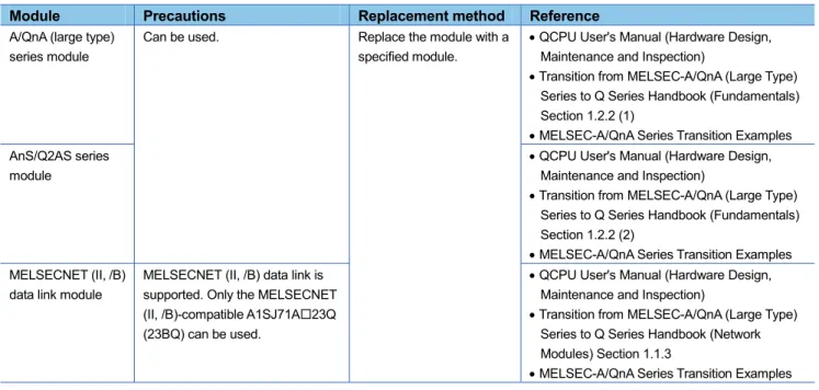
(1) When the serial number (first five digits) of the replaced Universal model QCPU is "13102" or later
Table 2.1 Precautions for using the A/QnA (large type) series modules
Module Precautions Replacement method Reference
A/QnA (large type) series module
Can be used. Replace the module with a specified module.
QCPU User's Manual (Hardware Design, Maintenance and Inspection)
Transition from MELSEC-A/QnA (Large Type) Series to Q Series Handbook (Fundamentals) Section 1.2.2 (1)
MELSEC-A/QnA Series Transition Examples AnS/Q2AS series
module
QCPU User's Manual (Hardware Design, Maintenance and Inspection)
Transition from MELSEC-A/QnA (Large Type) Series to Q Series Handbook (Fundamentals) Section 1.2.2 (2)
MELSEC-A/QnA Series Transition Examples MELSECNET (II, /B)
data link module
MELSECNET (II, /B) data link is supported. Only the MELSECNET (II, /B)-compatible A1SJ71A23Q (23BQ) can be used.
QCPU User's Manual (Hardware Design, Maintenance and Inspection)
Transition from MELSEC-A/QnA (Large Type) Series to Q Series Handbook (Network Modules) Section 1.1.3
Example 1) Module replacement
*1 To use the A/QnA series extension base units in the system after replacement, observe the following precautions.
The extension base units shall be connected in the following order: Q5B/Q6BQA1S5B/QA1S6BQA6BQA6ADP+A5B/A6B.
The QA1S6B cannot be used together with the QA6ADP+A5B/A6B.
Example 2) Network configuration
(2) When the serial number (first five digits) of the replaced Universal model QCPU is "13101" or
earlier
Table 2.2 Precautions for using the A/QnA (large type) series modules
Module Precautions Replacement method Reference
A/QnA (large type) series module
Cannot be used.
The following base units, for using A/QnA (large type) series modules, cannot be connected.
QA extension base unit
A series (large type) extension base unit + QA6ADP
QA1S extension base unit
A-A1S module conversion adapter (A1ADP-XY/SP)
Replace all modules with Q series modules.
Transition from
MELSEC-A/QnA (Large Type) Series to Q Series Handbook (Fundamentals) Section 1.2.2 (1)
MELSEC-A/QnA Series Transition Examples AnS/Q2AS series
module
Transition from
MELSEC-A/QnA (Large Type) Series to Q Series Handbook (Fundamentals) Section 1.2.2 (2)
MELSEC-A/QnA Series Transition Examples MELSECNET (II, /B)
data link module
MELSECNET (II, /B) data link is not supported. (The MELSECNET (II, /B)-compatible A1SJ71A23Q (23BQ) cannot be used.)
Use other network systems, such as CC-Link IE Controller Network, CC-Link IE Field Network, and MELSECNET/H(10).
Transition from
MELSEC-A/QnA (Large Type) Series to Q Series Handbook (Network Modules) Section 1.1.3
Example 1) Module replacement
*1 The replacement step 1, which is written in Section 1.2.2 of the Transition from MELSEC-A/QnA (Large Type) Series to Q Series Handbook (Fundamentals), is not available.
2.2
Use of the Q series large type base unit
When the Q series large type base unit, Q series large type I/O modules, and renewal tool manufactured by
Mitsubishi Electric Engineering Co., Ltd. are used, the terminal block of an existing A/QnA (large type) series
I/O module can be used without rewiring. This helps to reduce time for wiring.
Table 2.2 Precautions for using the Q series large type base unit
Module Precautions Replacement method Reference
Q series large type base unit
Can be used except the following cases:
When the Q00UJCPU is used
In multiple CPU configuration
No restrictions*1 Transition from
MELSEC-A/QnA (Large Type) Series to Q Series Handbook (Fundamentals) Section 1.2.2 (3)
MELSEC-A/QnA Series Transition Examples Renewal tool
manufactured by Mitsubishi Electric Engineering Co., Ltd.
No restrictions
(The Q series large type base unit can be used together.)
For details of specifications, precautions, and restrictions, contact your local Mitsubishi representative.
Transition from
MELSEC-A/QnA (Large Type) Series to Q Series Handbook (Fundamentals) Section 1.2.2 (4)
2.3 GOT
connection
Only GOT1000 series can be connected to the Universal model QCPU.
When GOT other than GOT1000 series is used, it must be replaced with GOT1000 series regardless of the
connection method.
Table 2.3 Precautions for GOT connection
Item Precautions Replacement method Reference
GOT connection
Only GOT1000 series can be connected to the Universal model QCPU regardless of the connection method (such as bus connection, CPU direct connection, and Ethernet connection).
Replace the connected GOT with GOT1000 series.
GOT1000 series can be connected by any connection methods including bus connection, CPU direct connection, and Ethernet connection.*1
GOT1000 Series Connection Manual (Mitsubishi Products)
*1 For the QnUDE(H)CPU, CPU direct connection is not available.
Product Model GT Designer2 OS version compatible with the Universal model QCPU*2 GT Works3 OS Version compatible with the Universal model QCPU*2
Used with Q00UJ/Q00U /Q01UCPU Used with Q02U/Q03UD/ Q04UDH/Q06 UDHCPU Used with Q13UDH/ Q26UDH CPU Used with Q10UDH/ Q20UDH CPU Used with Q03UDE/Q04U DEH/Q06UDEH /Q13UDEH/Q26 UDEHCPU Used with Q10UDEH/Q 20UDEHCPU
Used with High-speed Universal model QCPU
GOT1000 GT15-
GT11-
Version 2.91V or later Version 2.60N or later Version 2.76E or later Version 2.91V or later Version 2.81K or later Version 2.91V or later
Version 1.64S or later
GT10- Version 2. 91V or later
Version 2.76E or later Version 2.76E or later Version 2.91V or later Version 2.81K or later Version 2.91V or later
Version 1.64S or later
3. Utilizing
programs
The following section contains some instructions that cannot be converted into those for the Universal model
QCPU or instructions whose specifications differ from those for the Universal model QCPU.
(Relevant handbook)
Transition from MELSEC-A/QnA (Large Type) Series to Q Series Handbook (Fundamentals)
7.2 Instruction Conversion
This chapter explains instructions for the Universal model QCPU whose descriptions differ from those
described in the above section.
3.1
Sequence instructions requiring a review before replacing the ACPU
This section describes instructions requiring a review before replacing the ACPU with the Universal model
QCPU.
Table 3.1 Instructions requiring a review before replacing the ACPU (common instructions)
Symbol Instruction Replacing method Reference
PR Print ASCII code instruction It is recommended to use GOT as an ASCII code display device. ASCII codes stored in devices are directly displayed as characters on GOT.
Instructions can be replaced using a replacement program.
Section 3.1.1
PRC Print comment instruction It is recommended to use GOT as an ASCII code display device. Device comments can be displayed on GOT.
Comment data can be output to a display device in the replacement program of the PR instruction after reading data using the reading device comment data instruction (COMRD(P)).
Table 3.2 Instructions requiring a review before replacing the ACPU (AnA/AnU-dedicated instructions)
Symbol Instruction Replacing method Reference
IX Index modification of entire ladder
Use alternative programs. Section 3.2.1 IXEND
KEY Numerical key input instruction
It is recommended to use GOT as a numeral input device.
Instructions can be replaced using a replacement program.
3.1.1
Replacement example of the PR instruction
The following shows the example of a program for replacement using the PR instruction.
(1) Example of device assignment
(Before replacement) (After replacement)
Application Device Application Device Output string D0 to D3 Output string D0 to D3 ASCII code output signal Y100 to Y107 ASCII code output signal Y100 to Y107 Strobe signal Y108 Strobe signal Y108 In-execution flag Y109 In-execution flag Y109
Output string storage address (BIN32) D20 to D21 Output string storage address (BIN32)
(Used for sub-routine programs and interrupt programs)
D200 to D201
Number of output characters D202 Output module start Y number D203 Character extraction position D204 Number of extracted characters D205 String output status value D206 Result of string extraction by the MIDR
instruction
D207
String output in-execution flag M200 For index modification Z0
If the device numbers in the example above are used for other applications, assign unused device numbers
instead.
(3) Program after replacement
In the sequence program after replacement, three programs are required as shown below.
(a) Main routine program
Replace the PR instruction with the CALL instruction so that a subroutine program is called.
Output string storage device (‘D0’ in the program below) cannot be specified directly with the CALL
instruction.
Use the ADRSET instruction to acquire the indirect address for the CALL instruction.
Y device (‘Y100’ in the program before replacement shown in (2)) cannot be specified directly as output Y
number with the CALL instruction. Specify the output Y number in integer.
An interrupt program is used to output character codes via the output module. Enable the execution of
interrupt program using the EI instruction.
FEND
RET
IRET END Main routine program
Subroutine program
Interrupt program P1
I31
<After transition>
END Main routine program <Before transition>
Output strings and output string storage address are set.
Initial processing
(b) Subroutine program
In the subroutine program, the data for outputting ASCII codes using a fixed scan interrupt program (10ms)
are set to work devices. Also, the flag for activating the processing in the fixed scan interrupt program is
turned on.
Specify the following arguments for the subroutine program.
First argument Output string storage address (Input) Second argument Output module start Y number (Input)
Data specified by the CALL(P) arguments are saved. Output string storage address
Number of output strings Output module start number
Devices used for the string output processing of the interrupt program I31 are initialized.
Yn0 to Yn7 (ASCII code), Yn8 (strobe signal), and Yn9 (in-execution flag) are all turned OFF.
(c) Interrupt program
The following processing is added to a fixed scan interrupt program (10ms).
The fixed scan interrupt program outputs ASCII codes from the output module and controls the strobe signal.
The following signals are all turned OFF when all strings are output. Yn0 to Yn7 (ASCII code) Yn8 (strobe signal) Yn9 (in-execution flag)
Status 0:
One character is extracted from the output string using the MIDR instruction and output to the Y module. The strobe signal is turned OFF for 10ms.
Status 3:
The status value is returned to 0 since the output processing of one character is completed. The next character is extracted. Status 1:
The strobe signal is turned ON for 10ms.
Status 2:
The strobe signal is turned OFF for 10ms.
3.1.2
Replacement example of the KEY instruction
The following shows the example of a program for replacement using the KEY instruction.
(1) Example of device assignment
(Before replacement) (After replacement)
Application Device Application Device Numeric input execution instruction M0 Numeric input execution instruction M0 Input complete flag M1 Input complete flag M1
ASCII code input signal X100 to X107 Input data area D200 to D202 Number of input digits D10 ASCII code input signal X100 to X107 Data storage device D20 to D21 Strobe signal X108
Input data area address (BIN32) D210 to D211 (Input data area + 0) address (BIN32) D212 to D213 (Input data area + 1) address (BIN32) D214 to D215 (Input data area + 2) address (BIN32) D216 to D217 For shifting input data D218 For converting input data D219 to D220
If the device numbers in the example above are used for other applications, assign unused device numbers
instead.
(3) Program after replacement
In the sequence program after replacement, two programs are required as shown below.
(a) Main routing program
Set ‘0’ in the input data area on the rising edge of the execution instruction (‘M0’ in the program below) and
initialize the program.
Execute the CALL instruction on every rising edge of the strobe signal (‘X108’ in the program below) so that
a subroutine program is called.
In the subroutine program, input codes are added to the input data area and the completion status is
checked.
Pass the following data to the subroutine program at the execution of the CALL instruction.
ASCII code input value from the input module (Xn0 to Xn7)
Number of digits to be input.
Indirect address of the input data area (Use the ADRSET instruction to acquire the indirect address for
the input data area.)
Bit devices to be turned on when input is completed.
FEND
RET
END Main routine program
Subroutine program <After transition>
END Main routine program <Before transition>
Initial processing
ASCII code is added to the input data area. P2
The input data area is initialized.
(b) Subroutine program
In the subroutine program, ASCII codes specified by an argument are added to the input data area and the
completion status is checked.
Specify the following arguments for the subroutine program.
First argument ASCII code input from the input module (K2Xn) (Input) Second argument Number of digits to be input (Input) Third argument Indirect address of the input data area (Input) Fourth argument Bit device turned on when input is completed (Output)
Numeric entry is ended when the at-completion ON signal is ON or 0DH is input.
Addresses of the input data area are saved in the work devices.
The 1st to 4th digit numerals in (input data area +2) areshifted for one digit to the left.
Numeral entered in ASCII code is converted into one numeral in BIN data using the HABIN instruction.
The 5th to 8th digit numerals in (input data area +1) are shifted for one digit to the left and the converted numeral is set to the 8th digit.
The number of digits to be input in (input data area +0) is
incremented by one.
The at-completion ON signal is turned ON when the input processing for specified digits is completed.
3.2
Sequence instructions requiring a review before replacing the QnACPU
This section describes instructions requiring a review before replacing the QnACPU with the Universal model
QCPU.
Table 3.3 Instructions requiring a review before replacing the QnACPU
Symbol Instruction Replacing method Reference
IX Index modification of entire ladder
Use alternative programs. Section 3.2.1 IXEND
IXDEV Modification value specification in index modification of entire ladder
Change the program so that the device offset values specified by the IXSET instruction are directly set to the index modification table using the MOV instruction.
Section 3.2.2 IXSET
PR Print ASCII code instruction It is recommended to use GOT as an ASCII code display device. ASCII codes stored in devices are directly displayed as characters on GOT.
Instructions can be replaced using a replacement program.
Section 3.2.3
PRC Print comment instruction It is recommended to use GOT as an ASCII code display device. Device comments can be displayed on GOT.
Comment data can be output to a display device in the replacement program of the PR instruction after reading data using the reading device comment data instruction (COMRD(P)). CHKST Specific format failure check
instruction
Instructions can be replaced using a replacement program. Section 3.2.4 CHK
CHKCIR Format change instruction for CHK instruction
Failure detection ladder patterns can be changed in a replacement program.
CHKEND
PLOW Program low-speed execution registration instruction
Use the PSCAN instruction instead of this instruction when low-speed execution type programs are replaced with scan execution type programs.
No instruction can be used if low-speed execution type programs are replaced with fixed scan execution type programs.
-
PCHK Program execution status check instruction
Check a program execution status on the Program monitor list screen of GX Developer. For details, refer to Section 3.13.1 in the QnUCPU User's Manual (Function Explanation, Program Fundamentals).
KEY Numerical key input instruction It is recommended to use GOT as a numeral input device.
Instructions can be replaced using a replacement program.
3.2.1
Replacement example of the IX and IXEND instructions
A replacement example of program using the IX and IXEND instructions is shown below.
To save index register data using the ZPUSH instruction, a 23-word index register save area is required.
(1) Example of device assignment
(Before replacement) (After replacement)
Application Device Application Device Index modification table D100 to D115 Index modification table D100 to D115
Index register save area D200 to D222
If the device numbers in the example above are used for other applications, assign unused device numbers
instead.
(2) Program before replacement
The modification value set in the index modification table is added.
(3) Program after replacement
Replace the IX instruction with the ZPUSH instruction and set the contents of index modification table in
the to index register.
Replace the IXEND instruction with the ZPOP instruction.
Contents of the index modification table are set to the index registers Z0 to Z15.
Modification target (No change required)
The saved index register is restored. (Transition from the IXEND instruction) Current index register is
saved.
3.2.2
Replacement example of the IXDEV and IXSET instructions
The following shows the example of a program for replacement using the IXDEV and IXSET instructions.
Change the program so that the device offset values specified for the contacts between the IXDEV and IXSET
instructions are directly set to the index modification table using the MOV instruction.
For a device whose offset value is not specified by the IXDEV and IXSET instructions, set the value to 0 in the
program after replacement.
The following figure shows correspondence between device offset specification and index modification table
set by the IXDEV and IXSET instructions.
*1 Device numbers are represented in hexadecimal. Use hexadecimal constants (H) when setting values in the index modification table. *2 Start I/O numbers (U) are represented in hexadecimal. Use hexadecimal constants (H) when setting values in the index modification
table.
*3 Devices B, W, X, or Y can be specified following J\. Set device numbers for B, W, X, and Y as device offset values of each device in the index modification table.
For example, if ‘J10\Y220’ is specified by the IXDEV or IXSET instruction, set ‘K10’ in (D)+13 and ‘H220’ in (D)+3 in the replacement program. ((D) indicates the start device in the index modification table.)
IXSET (D)+0 (D)+1 (D)+2 (D)+3 (D)+4 (D)+5 (D)+6 (D)+7 (D)+8 (D)+9 (D)+10 (D)+11 (D)+12 (D)+13 (D)+14 (D)+15 Device offset specification by the IXDEV
and IXSET instructions Index modification table
Start I/O number
Buffer memory Timer
Counter
Input *1
Output *1
Internal relay
Latch relay
Edge relay
Link relay *1
Data register
Link register *1
File register
Intelligent function module device *2
Link direct device *3
File register (through number) Pointer T C X Y M L V B
D .XX
W .XX
R .XX
U \G .XX
J \B
ZR .XX
(1) Program before replacement
(2) Program after replacement
The device offset values for input (X), output (Y), internal relay (M), data register (D), link register (W), and pointer (P) are set to the index modification table starting from D0.
3.2.3
Replacement example of the PR instruction
The following shows the example of a program for replacement using the PR instruction.
The number of output characters can be switched by turning on/off SM701.
(1) Example of device assignment
(Before replacement) (After replacement)
Application Device Application Device Output string D0 to D3 Output string D0 to D3 ASCII code output signal Y100 to Y107 ASCII code output signal Y100 to Y107 Strobe signal Y108 Strobe signal Y108 In-execution flag Y109 In-execution flag Y109
Output string storage address (BIN32) D20 to D21 Output string storage address (BIN32)
(Used for sub-routine programs and interrupt programs)
D200 to D201
Number of output characters D202 Output module start Y number D203 Character extraction position D204 Number of extracted characters D205 String output status value D206 Result of string extraction by the MIDR
instruction
D207
String output in-execution flag M200 For index modification Z0
If the device numbers in the example above are used for other applications, assign unused device numbers
instead.
(3) Program after replacement
In the sequence program after replacement, three programs are required as shown below.
(a) Main routine program
Replace the PR instruction with the CALL instruction so that a subroutine program is called.
Output string storage device (‘D0’ in the program below) cannot be specified directly with the CALL
instruction.
Use the ADRSET instruction to acquire the indirect address for the CALL instruction.
Y device (‘Y100’ in the program before replacement shown in (2)) cannot be specified directly as output Y
number with the CALL instruction. Specify the output Y number in integer.
An interrupt program is used to output character codes via the output module. Enable the execution of
interrupt program using the EI instruction.
FEND
RET
IRET END Main routine program
Subroutine program
Interrupt program P1
I31
<After transition>
END Main routine program <Before transition>
Output strings and output string storage address are set.
Initial processing
(b) Subroutine program
In the subroutine program, the data for outputting ASCII codes using a fixed scan interrupt program (10ms)
are set to work devices. Also, the flag for activating the processing in the fixed scan interrupt program is
turned on.
Specify the following arguments for the subroutine program.
First argument Output string storage address (Input) Second argument Output module start Y number (Input)
Data specified by the CALL(P) arguments are saved. Output string storage address
Number of output strings Output module start number
Devices used for the string output processing of the interrupt program I31 are initialized.
Yn0 to Yn7 (ASCII code), Yn8 (strobe signal), and Yn9 (in-execution flag) are all turned OFF.
(c) Interrupt program
The following processing is added to a fixed scan interrupt program (10ms).
The fixed scan interrupt program outputs ASCII codes from the output module and controls the strobe signal.
The following signals are all turned OFF when all strings are output. Yn0 to Yn7 (ASCII code) Yn8 (strobe signal) Yn9 (in-execution flag)
Status 0:
One character is extracted from the output string using the MIDR instruction and output to the Y module. The strobe signal is turned OFF for 10ms.
Status 3:
The status value is returned to 0 since the output processing of one character is completed. The next character is extracted. Status 1:
The strobe signal is turned ON for 10ms.
Status 2:
The strobe signal is turned OFF for 10ms.
3.2.4
Replacement example of the CHKST and CHK instructions
The following shows the example of a program for replacement using the CHKST and CHK instructions.
In the example below, if the replacement program for the CHKST and CHK instructions detects failure, the
failure number (contact number + coil number) is stored in D200 and the annunciator F200 turns on.
(1) Example of device assignment
(Before replacement) (After replacement)
Application Device Application Device Advance end detection sensor
input 1
X100 Advance end detection sensor input 1 X100
Retract end detection sensor input 1
X101 Retract end detection sensor input 1 X101
Advance end detection sensor input 2
X102 Advance end detection sensor input 2 X10²
Retract end detection sensor input 2
X103 Retract end detection sensor input 2 X10³
Advance end detection sensor input 3
X104 Advance end detection sensor input 3 X10⁴
Retract end detection sensor input 3
X105 Retract end detection sensor input 3 X10⁵
Advance end detection sensor input 4
X106 Advance end detection sensor input 4 X10⁶
Retract end detection sensor input 4
X107 Retract end detection sensor input 4 X10⁷
Failure detection output 1 Y100 Failure detection output 1 Y100 Failure detection output 2 Y102 Failure detection output 2 Y102 Failure detection output 3 Y104 Failure detection output 3 Y104 Failure detection output 4 Y106 Failure detection output 4 Y106 Coil number (failure type detected) D100
Contact number D101
Failure number D200
Failure detection display F200 For index modification Z0
If the device numbers in the example above are used for other applications, assign unused device numbers
instead.
When the advance end detection sensor input performs a failure detection of Xn, assign device numbers for
the retract end detection sensor input and the failure detection output as described below.
Advance end detection sensor input
Xn
Retract end detection sensor input
Xn+1
(2) Program before replacement
(3) Program after replacement
In the sequence program after replacement, two programs are required as shown below.
(a) Main routine program
Replace the CHKST and CHK instructions with the CALL instructions so that a subroutine program is
called.
One CALL instruction is required for each device specified as check condition before the CHK instruction.
(In the program before replacement shown in (2), four CALL instructions need to be added since there are
four check conditions before the CHK instruction.)
Device number and contact number of X devices (check condition) are specified in each CALL instruction.
Contact number is used to display failure number when a failure is detected.
FEND
RET END Main routine program
Subroutine program <After transition>
END Main routine program <Before transition>
Initial processing
An failure status is checked, and if a failure is detected, a failure number is stored in D200.
(b) Subroutine program
In the subroutine program, a failure status is checked using a failure detection ladder pattern.
If a failure is detected, a failure number is stored in D200 and the annunciator F200 is turned on.
Specify the following arguments for the subroutine program.
First argument Device number of X device targeted for failure check (Input) Second argument Contact number of X device targeted for failure check (Input)
(4) Replacement method when failure detection ladder patterns are changed by the CHKCIR and
CHKEND instructions
Failure detection ladder patterns can be changed in the subroutine program described in (3).
<Failure detection target> If a failure is detected, the coil number corresponding to the failure type is set to D100.
3.2.5
Replacement example of the KEY instruction
The following shows the example of a program for replacement using the KEY instruction.
(1) Example of device assignment
(Before replacement) (After replacement)
Application Device Application Device Numeric input execution instruction M0 Numeric input execution instruction M0 Input complete flag M1 Input complete flag M1
Input data area D200 to D203 Input data area D200 to D202 ASCII code input signal X100 to X107 ASCII code input signal X100 to X107 Strobe signal X108 Strobe signal X108
Input data area address (BIN32) D210 to D211 (Input data area + 0) address (BIN32) D212 to D213 (Input data area + 1) address (BIN32) D214 to D215 (Input data area + 2) address (BIN32) D216 to D217 For shifting input data D218 For converting input data D219 to D220
If the device numbers in the example above are used for other applications, assign unused device numbers
instead.
(3) Program after replacement
In the sequence program after replacement, two programs are required as shown below.
(a) Main routing program
Set ‘0’ in the input data area on the rising edge of the execution instruction (‘M0’ in the program below) and
initialize the program.
Execute the CALL instruction on every rising edge of the strobe signal (‘X108’ in the program below) so that
a subroutine program is called.
In the subroutine program, input codes are added to the input data area and the completion status is
checked.
Pass the following data to the subroutine program at the execution of the CALL instruction.
ASCII code input value from the input module (Xn0 to Xn7)
Number of digits to be input.
Indirect address of the input data area (Use the ADRSET instruction to acquire the indirect address for
the input data area.)
Bit devices to be turned on when input is completed.
FEND
RET
END Main routine program
Subroutine program <After transition>
END Main routine program <Before transition>
Initial processing
ASCII code is added to the input data area. P2
The input data area is initialized.
(b) Subroutine program
In the subroutine program, ASCII codes specified by an argument are added to the input data area and the
completion status is checked.
Specify the following arguments for the subroutine program.
First argument ASCII code input from the input module (K2Xn) (Input) Second argument Number of digits to be input (Input) Third argument Indirect address of the input data area (Input) Fourth argument Bit device turned on when input is completed (Output)
Numeric entry is ended when the at-completion ON signal is ON or 0DH is input.
Addresses of the input data area are saved in the work devices.
The 1st to 4th digit numerals in (input data area +2) areshifted for one digit to the left.
Numeral entered in ASCII code is converted into one numeral in BIN data using the HABIN instruction.
The 5th to 8th digit numerals in (input data area +1) are shifted for one digit to the left and the converted numeral is set to the 8th digit.
The number of digits to be input in (input data area +0) is
incremented by one.
The at-completion ON signal is turned ON when the input processing for specified digits is completed.
3.3 SFC
(MELSAP-II/MELSAP3)
3.3.1
Functions requiring a review before replacing the ACPU with SFC (MELSAP-II)
If the ACPU with SFC (MELSAP-II) is replaced by the Universal model QCPU, some functions of the ACPU
will be unavailable.
The following table shows the functions unavailable for the Universal model QCPU.
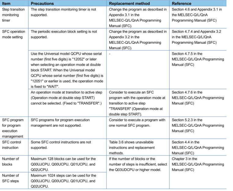
Table 3.4 Functions unavailable for the Universal model QCPU
Item Precautions Replacement method Reference
Step transition monitoring timer
The step transition monitoring timer is not supported.
Change the program as described in Appendix 3.1 in the
MELSEC-Q/L/QnA Programming Manual (SFC).
Section 4.6 and Appendix 3.1 in the MELSEC-Q/L/QnA Programming Manual (SFC)
Number of blocks
Maximum 128 blocks can be used for the Q00UJCPU, Q00UCPU, Q01UCPU, and Q02UCPU.
If the number of blocks or the number of steps is insufficient, select the Q03UDCPU or higher model.
Chapter 3 in the
3.3.2
Functions and instructions requiring a review before replacing the QnACPU with SFC
(MELSAP3)
If the QnACPU with SFC (MELSAP-3) is replaced by the Universal model QCPU, some functions and some
SFC control instructions of the QnACPU will be unavailable.
The following tables show the functions and SFC control instructions unavailable for the Universal model
QCPU.
Table 3.5 Functions unavailable for the Universal model QCPU
Item Precautions Replacement method Reference
Step transition monitoring timer
The step transition monitoring timer is not supported.
Change the program as described in Appendix 3.1 in the
MELSEC-Q/L/QnA Programming Manual (SFC).
Section 4.6 and Appendix 3.1 in the MELSEC-Q/L/QnA Programming Manual (SFC)
SFC operation mode setting
The periodic execution block setting is not supported.
Change the program as described in Appendix 3.2 in the
MELSEC-Q/L/QnA Programming Manual (SFC).
Section 4.7.4 and Appendix 3.2 in the MELSEC-Q/L/QnA Programming Manual (SFC)
Use the Universal model QCPU whose serial number (first five digits) is "12052" or later when selecting an operation mode at double block START. When the Universal model QCPU whose serial number (first five digits) is "12051" or earlier is used, the operation mode is fixed to "WAIT".
- Section 4.7.5 in the
MELSEC-Q/L/QnA Programming Manual (SFC)
An operation mode at transition to active step (Operation mode at double step START) cannot be selected. (Fixed to "TRANSFER".)
Consider to execute an SFC program with the operation mode at transition to active step
"TRANSFER" (Operation mode at double step START).
Section 4.7.6 in the
MELSEC-Q/L/QnA Programming Manual (SFC) SFC program for program execution management
SFC programs for program execution management are not supported.
Consider to execute a program with one normal SFC program.
Section 5.2.3 in the
MELSEC-Q/L/QnA Programming Manual (SFC)
SFC control instruction
Some SFC control instructions are not supported.
Table 3.6 shows unavailable instructions and replacement methods.
Section 4.4 in the
MELSEC-Q/L/QnA Programming Manual (SFC)
Number of blocks
Maximum 128 blocks can be used for the Q00UJCPU, Q00UCPU, Q01UCPU, and Q02UCPU.
If the number of blocks or the number of steps is insufficient, select the Q03UDCPU or higher model.
Chapter 3 in the
MELSEC-Q/L/QnA Programming Manual (SFC)
Number of SFC steps
Table 3.6 SFC control instructions unavailable for the Universal model QCPU
Symbol Instruction Alternative method Reference
LD TRn Forced transition check instruction
When the programmable controller type is changed, these instructions are converted into SM1255.
Modify programs as needed.
- AND TRn
OR TRn LDI TRn ANDI TRn ORI TRn LD BLm\TRn AND BLm\TRn OR BLm\TRn LDI BLm\TRn ANDI BLm\TRn ORI BLm\TRn
SCHG(D) Active step change instruction
Refer to Appendix 3 "Restrictions on Basic Model QCPU, Universal Model QCPU, and LCPU and Alternative Methods" in the MELSEC-Q/L/QnA Programming Manual (SFC).
The MELSEC-Q/L/QnA Programming Manual (SFC) SET TRn Transition control
instruction SET BLm\TRn
RST TRn RST BLm\TRn
BRSET(S)*1 Block switching
instruction
When the programmable controller type is changed, these instructions are converted into SM1255.
Modify programs as needed.
4. Precautions for the performance and specifications of the CPU modules
An A/QnA (large type) series CPU and a Universal model QCPU partly differ in performance and
specifications.
This chapter describes precautions for the performance and specifications of the CPU modules.
4.1
Precautions for performance and specifications when the ACPU is replaced
Table 4.1 Precautions for performance and specifications when the ACPU is replaced
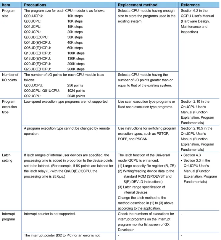
Item Precautions Replacement method Reference
Program size
The program size for each CPU module is as follows: Q00UJCPU: 10K steps Q00UCPU: 10K steps Q01UCPU: 15K steps Q02UCPU: 20K steps Q03UD(E)CPU: 30K steps Q04UD(E)HCPU: 40K steps Q06UD(E)HCPU: 60K steps Q10UD(E)HCPU: 100K steps Q13UD(E)HCPU: 130K steps Q20UD(E)HCPU: 200K steps Q26UD(E)HCPU: 260K steps
Select a CPU module having enough size to store the programs used in the existing system.
Section 6.2 in the QCPU User's Manual (Hardware Design, Maintenance and Inspection)
Number of I/O points
The number of I/O points for each CPU module is as follows:
Q00UJCPU: 256 points Q00UCPU, Q01UCPU: 1024 points
Q02UCPU: 2048 points
Select a CPU module having the number of I/O points greater than or equal to that of the existing system.
Latch setting
If latch ranges of internal user devices are specified, the processing time is added in proportion to the device points set to be latched. (For example, if 8K points are latched for the latch relay (L) with the QnUD(E)(H)CPU, the
processing time is 28.6μs.)
The latch function of the Universal model QCPU is enhanced.
(1) Large-capacity file register (R, ZR) (2) Writing/reading device data to the
standard ROM (SP.DEVST and S(P).DEVLD instructions) (3) Latch range specification of
internal devices
Change the latch method to the method described in (1) to (3) above according to the application.
Section 4.3
Section 3.3 in the QnUCPU User's Manual (Function Explanation, Program Fundamentals) Interrupt program
Interrupt counter is not supported. Check the numbers of executions for interrupt programs on the Interrupt program monitor list screen of GX Developer.
-
SM/SD Use the Universal model QCPU whose serial number (first five digits) is "10102" or later when using the A
series-compatible special relay and special register (SM1000 to SM1255/SD1000 to SD1255). When the Universal model QCPU whose serial number (first five digits) is "10101" or earlier is used, replace them with the Universal model QCPU-compatible special relay and special register by using the conversion function of a programming tool. Note, however, that the ones which are not compatible with the Universal model QCPU are replaced with SM1255 and SD1255. Modify programs as needed.
Item Precautions Replacement method Reference
Processing time
Scan time and other processing times are different. Modify programs as needed, checking the processing timing.
-
MC protocol (dedicated protocol)
The following frame types cannot be used when accessing the Universal model QCPU.*1
A-compatible 1C frame
A-compatible 1E frame
Use the frame types below.
QnA-compatible 2C/3C/4C frame
QnA-compatible 3E frame
4E frame
MELSEC-Q/L MELSEC Communication Protocol Reference Manual
The following commands cannot specify monitoring conditions.
Randomly reading data in units of word (Command: 0403)
Device memory monitoring (Command: 0801) The applicable frame types are as follows:
QnA-compatible 3C/4C frame
QnA-compatible 3E frame
4E frame
-
LED indication priority setting
LED indication priority cannot be set. Only LED indication setting at error occurrence is supported.
- Section 3.20.2 in the QnUCPU User's Manual (Function Explanation, Program Fundamentals) Others Specifications including the processing time of instructions and processing methods of timer and
counter depend on the CPU module.
The scan time and activation timing of interlock signals may depend on the performance, specifications, and functions of the CPU module.
After starting a system after replacement, check operations of the whole system first and then move to the actual operation.
-
4.2
Precautions for performance and specifications when the QnACPU is replaced
Table 4.2 Precautions for performance and specifications when the QnACPU is replaced
Item Precautions Replacement method Reference
Program size
The program size for each CPU module is as follows: Q00UJCPU: 10K steps Q00UCPU: 10K steps Q01UCPU: 15K steps Q02UCPU: 20K steps Q03UD(E)CPU: 30K steps Q04UD(E)HCPU: 40K steps Q06UD(E)HCPU: 60K steps Q10UD(E)HCPU: 100K steps Q13UD(E)HCPU: 130K steps Q20UD(E)HCPU: 200K steps Q26UD(E)HCPU: 260K steps
Select a CPU module having enough size to store the programs used in the existing system.
Section 6.2 in the QCPU User's Manual (Hardware Design, Maintenance and Inspection)
Number of I/O points
The number of I/O points for each CPU module is as follows:
Q00UJCPU: 256 points Q00UCPU, Q01UCPU: 1024 points
Q02UCPU: 2048 points
Select a CPU module having the number of I/O points greater than or equal to that of the existing system.
Program execution type
Low-speed execution type programs are not supported. Use scan execution type programs or fixed scan execution type programs.
Section 2.10 in the QnUCPU User's Manual (Function Explanation, Program Fundamentals) A program execution type cannot be changed by remote
operation.
Use instructions for switching program execution types, such as PSTOP, POFF, and PSCAN.
Section 2.10.5 in the QnUCPU User's Manual (Function Explanation, Program Fundamentals) Latch setting
If latch ranges of internal user devices are specified, the processing time is added in proportion to the device points set to be latched. (For example, if 8K points are latched for the latch relay (L) with the QnUD(E)(H)CPU, the
processing time is 28.6μs.)
The latch function of the Universal model QCPU is enhanced.
(1) Large-capacity file register (R, ZR) (2) Writing/reading device data to the
standard ROM (SP.DEVST and S(P).DEVLD instructions) (3) Latch range specification of
internal devices
Change the latch method to the method described in (1) to (3) above according to the application.
Section 4.3
Section 3.3 in the QnUCPU User's Manual (Function Explanation, Program Fundamentals) Interrupt program
Interrupt counter is not supported. Check the numbers of executions for interrupt programs on the Interrupt program monitor list screen of GX Developer.
-
The interrupt pointer (I32 to I40) for an error is not supported.
- -
ZPUSH instruction
The number of index registers is increased to 20 for the Universal model QCPU. The area for saving the data in the index register with the ZPUSH instruction is increased as well.
Increase the save areas used for the ZPUSH instruction as needed.
Item Precautions Replacement method Reference File usability setting for each program
The following file usability setting for each program is not available.*1
File register
Initial device value
Comment
When file usability has been set, modify the program.
Section 2.10 in the QnUCPU User's Manual (Function Explanation, Program Fundamentals) SM/SD Usage of a part of the special relay and special register is
different.
Check the specifications of the special relay and special register and modify the program as needed.
Appendix 2 and Appendix 3 in the QCPU User's Manual (Hardware Design, Maintenance and Inspection) Use the Universal model QCPU whose serial number (first
five digits) is "10102" or later when using the A series-compatible special relay and special register (SM1000 to SM1255/SD1000 to SD1255). When the Universal model QCPU whose serial number (first five digits) is "10101" or earlier is used, replace them with the Universal model QCPU-compatible special relay and special register by using the conversion function of a programming tool. Note, however, that the ones which are not compatible with the Universal model QCPU are replaced with SM1255 and SD1255. Modify programs as needed.
-
Processing time
Scan time and other processing times are different. Modify programs as needed, checking the processing timing.
-
Module service interval time read
The module service interval time cannot be read. - -
MC protocol (dedicated protocol)
The following frame types cannot be used when accessing the Universal model QCPU. *2
A-compatible 1C frame
A-compatible 1E frame
Use the frame types below.
QnA-compatible 2C/3C/4C frame
QnA-compatible 3E frame
4E frame
MELSEC-Q/L MELSEC Communication Protocol Reference Manual
The following commands cannot specify monitoring conditions.
Randomly reading data in units of word (Command: 0403)
Device memory monitoring (Command: 0801) The applicable frame types are as follows:
QnA-compatible 3C/4C frame
QnA-compatible 3E frame
4E frame
-
Error history
Error history data cannot be stored in the memory card. The Universal model QCPU stores all storable data (up to 100) in the built-in memory.
Section 3.18 in the QnUCPU User's Manual (Function Explanation, Program Fundamentals) LED indication priority setting
LED indication priority cannot be set. Only LED indication setting at error occurrence is supported.
Item Precautions Replacement method Reference
Monitor*3 The monitoring condition cannot be set. Use the sampling trace function for checking device data under the specified monitoring condition. With this function, changes of the specified device data can be recorded at the following timings:
at the execution of the specified step
at the rising/falling edge of bit devices
when the value of word devices coincide with the setting value
at every specified time (settable range: 1ms to 5000ms)
Section 3.11.1 and 3.14 in the QnUCPU User's Manual (Function Explanation, Program Fundamentals)
Others Specifications including the processing time of instructions and processing methods of timer and counter depend on the CPU module.
The scan time and activation timing of interlock signals may depend on the performance, specifications, and functions of the CPU module.
After starting a system after replacement, check operations of the whole system first and then move to the actual operation.
-
*1 The local device file usability setting is also not available for the Universal model QCPU if the serial number (first five digits) is "10011" or earlier.
*2 Applicable to the Q02UCPU, Q03UDCPU, Q04UDHCPU, Q06UDHCPU, Q13UDHCPU, and Q26UDHCPU if the serial number (first five digits) is "10101" or earlier.
4.3 Device
latch
function
The device latch function
*1for the Universal model QCPU is more enhanced compared to that for the A/QnA
(large type) series CPU.
This section describes the enhanced device latch function in the Universal model QCPU.
*1 The latch function is used to hold device data even when the CPU module is powered off or reset.
(1) Device data latch methods
Device data of the Universal model QCPU can be latched by:
using a large-capacity file register (R, ZR),
writing/reading device data to/from the standard ROM (with the SP.DEVST and S(P).DEVLD instructions),
or
specifying a latch range of internal user devices.
(2) Details of each latch method
(a) Large-capacity file registers (R, ZR)
File register size is larger and processing speed is higher in the Universal model QCPU, compared to the
A/QnA (large type) series CPU.
To latch a lot of data (many device points), use of a file register is effective.
Table 4.3 shows capacities of file registers for each CPU module.
Table 4.3 File register size available for each CPU module
Model File register (R, ZR) size in the standard RAM
Q00UCPU, Q01UCPU, and Q02UCPU 64K points Q03UDCPU and Q03UDECPU 96K points Q04UDHCPU and 04UDEHCPU 128K points Q06UDHCPU and 06UDEHCPU 384K points Q10UDHCPU, Q10UDEHCPU, Q13UDHCPU and Q13UDEHCPU 512K points Q20UDHCPU, Q20UDEHCPU, Q26UDHCPU and Q26UDEHCPU 640K points
(b) Writing/reading device data to/from the standard ROM (SP.DEVST/S(P).DEVLD instructions)
Device data of the Universal model QCPU can be latched using the SP.DEVST and S (P).DEVLD instructions
(instructions for writing/reading data to/from the standard ROM).
(c) Specifying the latch range of internal user devices
Device data of the Universal model QCPU can be latched by specifying a latch range of internal user devices
in the same way as for the A/QnA (large type) series CPU.
The ranges can be set in the Device tab of the PLC parameter dialog box.
Internal user devices that can be latched are as follows:
Latch relay (L)
Link relay (B)
Annunciator (F)
Edge relay (V)
Timer (T)
Retentive timer (ST)
Counter (C)
Data register (D)
Link register (W)
POINT
If latch ranges of internal user devices are specified in the Universal model QCPU, the processing time
will increase in proportion to the points of the device to be latched. (For example, if 8K points are latched
for the latch relay (L) with the QnUD(E)(H)CPU, the processing time is 28.6
μ
s.)
To shorten the scan time, remove unnecessary latch device points to minimize the latch range.
The scan time will not increase when a latch range of the file register (R, ZR) is specified.
(3) How to shorten the scan time
When data to be latched are stored in a file register (R or ZR), the processing time is shorter than that for
latching internal user device.
Example Reducing the latch points of the data register (D) from 8K points to 2K points, and using the file
register (ZR) instead (when the Q06UDVCPU is used).
Table 4.4 Differences between before and after moving latch points of the data register (D) to the file register
(ZR)
Item Before After
Latch points for data register (D) 8192 (8K) points 2048 (2K) points
(6K points are moved to file register.)
Number of devices in the program Data register (D) (Latch range) 400 100 File register (ZR) (Standard RAM) 0 300 Additional scan time 0.37ms 0.11ms*1
REVISIONS
Version Print Date Revision
- December 2009 First edition
A July 2011 The descriptions of the reference manuals or the references have been changed in accordance with the composition changes of the manuals.
B December 2011 Revision on the new functions of the Universal model QCPU whose serial number (first five digits) is "13102" or later.
C December 2011 Precautions for using MELSECNET (II, /B) data link modules in Section 2.1 (1) (Table 2.1 and Example 2) are corrected.