A Synthesis Method to Propagate
False Path Information from RTL to Gate Level
Satoshi Ohtake Hiroshi Iwata Hideo Fujiwara
Graduate School of Information Science, Nara Institute of Science and Technology 8916-5 Takayama, Ikoma, Nara 630-0192, Japan
E-mail: {ohtake, hiroshi-i, fujiwara}@is.naist.jp
Abstract—This paper proposes a new synthesis method for propagating information of paths from register transfer level (RTL) to gate level. The method enables false path identification at RTL without not only enforcing strong constraints on logic synthesis but also loss of the information about false paths identified. Experiments show that the proposed method can reduce hardware and timing overhead and improve propagability of false path information through logic synthesis compared with the previous methods.
I. INTRODUCTION
Establishing correspondence between an RTL circuit and its synthesized gate level circuit is important for design and test of VLSI circuits. Correspondence between paths in the RTL circuit and that in the gate level circuit, which is dealt with in this paper, is valuable for improving performance and timing correctness of the circuit. Especially, the false path information is very valuable for design and test of circuits; it can be used for reducing time required for logic synthesis, improving circuit performance, test generation and test application and circuit area, as well as minimizing over-testing.
Although several false path identification methods at gate level [1]-[5] have been proposed, it is difficult to apply these method to large circuits containing a tremendous number of paths. There are methods to identify false paths by utilizing RTL design information [6]-[8] which can reduce time re- quired for identification several orders of magnitude. However, these are feasible only if RTL paths can be mapped into gate level paths. RTL path is represented by specifying RTL signal lines through which the path goes. The RTL path is mapped to gate level paths such that finding gate level signal lines corresponding to RTL signal lines composing the RTL path and then listing the gate level paths that go through the gate level signal lines. Until now, there are two ways to make the correspondence available: (1) employing restricted logic synthesis, called module interface preserving-logic synthesis (MIP-LS)[6], which maintains all the signal lines surrounding RTL modules during the transformation from RTL to gate level and preserves complete mapping between RTL paths and gate level ones by paying area and timing overhead and (2) finding mapping between RTL paths and gate level ones by considering functional equivalence between them without restriction on logic synthesis, which is referred to as module interface breaking-logic synthesis (MIB-LS), at the sacrifice on the completeness of the mapping [9].
In this paper, a new synthesis method, called mapping point preserving-logic synthesis (MPP-LS), is proposed to establish complete mapping between paths in an RTL circuit and its synthesized gate level circuit with a few restriction on logic synthesis. In the proposed method, unlike MIP-LS which preserves all the interfaces of modules in the RTL circuit, only the minimum number of mapping points, which are sufficient to distinguish any path from the others, are preserved. If false paths are identified at RTL before synthesize the circuit, the proposed method can further reduce the number of mapping points such that the preserved mapping points are sufficient to distinguish only the false paths from the others. On the other hand, unlike MIB-LS which does not guarantee establishing mapping between RTL paths and gate level ones, our proposed method can do.
Experiments for benchmark circuits show that the proposed method can reduce hardware and timing overhead by reducing mapping points which is to be preserved. Furthermore, timing margins of the synthesized circuits with MPP-LS are large compared with that with MIP-LS and are compatible with that with MIB-LS.
II. PRELIMINARIES
A. Circuit model
In this paper, we only consider structural RTL designs. A structural RTL design consists of a controller represented by a combinational logic block (CL) and a state register (SR), and a data path represented by RTL modules and signal lines connecting them, where an RTL module is an operational module, a register or a MUX and a signal line has an arbitrary bit width.
Primary inputs and outputs and registers at RTL are usually preserved during logic synthesis for structural RTL designs. To clarify the discussions in this paper, we assume that there exists one-to-one correspondence between bits of them and gate level primary inputs and outputs and flip-flops.
B. Gate level and RTL path representation
A gate level path pG= {eG1, . . . ,eGn} is an ordered set of gate level signal lines, where eG1 is the signal line directly connected to a primary input or the output of an FF, eGn is the signal line directly connected to a primary output or the input of an FF, and eGi (i = 2, . . . , n − 1) is the signal line connecting
978-1-4244-6613-9/10/$26.00 ©2010 IEEE 197
13th IEEE Int. Symp. on Design and Diagnostics of Electronic Circuits and Systems, pp.197-200, April 2010.
the gates having eGi−1 as an input and eGi+1 as an output. A subset of pG is called a sub gate level path of pG.
An RTL segment pR= {eR1, . . . ,eRn} is an ordered set of RTL signal lines, where eRi(i = 2, . . . , n − 1) is the RTL signal line connecting the modules having eRi−1 as an input and eRi+1 as an output. Especially, the RTL segment pRis called RTL path if eR1 is the RTL signal line directly connected to a primary input or the output of a register and eRn is the RTL signal line directly connected to a primary output or the input of a register. A subset of pR is called a sub RTL path of pR.
A reconvergent segment pair is a pair of segments pR= {eR1, . . . ,eRn} and qR = {d1R, . . . ,dmR}, where eR1 = dR1 and eRn = dmR. A fanin segment pair is a pair of segments pR= {eR1, . . . ,eRn} and qR= {d1R, . . . ,dmR} where eRn= dmR and eRi ̸= dRj(1 ≤ i < n, 1 ≤ j < m). A fanout segment pair is a pair of segments pR= {eR1, . . . ,eRn} and qR= {d1R, . . . ,dmR} where eR1= d1R and eRi ̸= dRj(1 < i ≤ n, 1 < j ≤ m).
An RTL signal line consists of one-bit signal lines. For an RTL signal line s, each one bit signal line separated from s is referred to as a bit-sliced RTL signal line of s. The i-th bit of s is represented as s[i]. A bit-sliced RTL path q = {eR1[k1], . . . , eRn[kn]}is an ordered set of bit-sliced RTL signal lines, where eR1[k1] is the k1-th bit-sliced RTL signal line directly connected to a primary input or the output of a register, eRn[kn] is the kn-th bit-sliced RTL signal line directly connected to a primary output or the input of a register, and eRi[ki](i = 2, . . . , n − 1) is the ki-th bit-sliced RTL signal line connecting the modules having eRi−1[ki−1] as an input and eRi+1[ki+1] as an output. A subset of q is called a sub bit-sliced RTL path of q.
C. Relation between paths
Functional equivalence between the sub bit-sliced RTL path and sub gate level path is defined as follows.
Definition 1 (Functionally equivalent path [9]): Sub bit-sliced RTL paths and sub gate level paths are simply referred to as sub paths. Sub paths q1= {e11, . . . ,e1n} and
q2= {e21, . . . ,e2m} are functionally equivalent if q1 and q2
satisfy the following conditions. 1) n= m
2) e1i ≡l e2i (i = 1, . . . , n), where ≡l denotes functional equivalence between the signal lines [9].
✷ For specifying an RTL path, it may be sufficient to represent the path using a sub RTL path. The following is the property of a sub RTL path that identifies an RTL path uniquely.
Definition 2 (Identification of path): [9] A sub RTL path qR is said to uniquely identify an RTL path pR if pR is the only path that properly includes qR. ✷ A set of RTL siganl lines may represent multiple RTL paths. This property can be utilized to specify a set of RTL paths by using a set of RTL signal lines. In this paper, we provide the following definition for unique identification of a set of paths. Definition 3 (Identification of path set): A set of RTL sig- nal lines SR is said to uniquely identify a set of RTL paths, PR, if PR is the only set of RTL paths that properly includes
all the maximum sub RTL paths composed by the RTL signal
lines in SR. ✷
Examples for definitions 2 and 3 are provided in the subsection III-C.
III. PROPOSEDMETHOD
A. Path mapping
The method of path mapping [9] is used to establish correspondence between a set of RTL paths in a given RTL circuit and its corresponding gate level paths in a synthesized gate level circuit with MIB-LS. For a given set of RTL paths, the method proceeds as follows.
1) Select minimum set of RTL signal lines that uniquely identify the given set of RTL paths (described in the subsection III-C).
2) Map bit-sliced RTL signal lines composing each RTL signal line on the sub RTL paths (this is called signal line mapping).
a) Find candidates of the functionally equivalent sig- nal lines in the gate level circuit by using a diagnostics technique [10].
b) Check the equivalence between each bit-sliced RTL signal line and its corresponding candidates and inequivalent candidates are discarded. 3) Represent gate level paths corresponding to the given
set of RTL paths so that listing mapped gate level signal lines through which the gate level paths pass.
Note that, in the original procedure of 1), multiple paths which have the same starting and ending points are dealt with at a turn. In this work, we improved the procedure so that any combination of multiple paths can be handled at a time. If signal line mapping fails, another RTL signal lines are tried to identify the given paths, iteratively.
B. Mapping point preservation during logic synthesis Commercial logic synthesis tools usually support to pre- serve specific RTL signal lines during optimization for engi- neering change or IP implantation in the downstream of de- sign flow. For DesignCompiler (Synopsys), “set dont touch” option can be used to preserve RTL signal lines. We can utilize this kind of tools for implementing MPP-LS.
By using MPP-LS, for each bit-sliced signal line on the RTL path, its functionally equivalent signal line in the gate level circuit that synthesized by MPP-LS is automatically derived. Therefore, during the path mapping, procedures 1) and 2) can be skipped. It means that unnecessary iteration of trial which may occur when using MIB-LS can be omitted.
C. Extraction of minimum set of RTL signal lines
By considering one of the minimum sets of RTL signal lines identifying a given set of RTL paths to be propagated to gate level, the number of mapping points to be preserved will be further reduced. In this paper, we propose a method to extract minimum RTL signal lines to be preserved from the given set of RTL paths.
198
!
"
#
$
%
& '
()*
+, - .
/
0 1
* 2
3
456)7)86)09:.629!;<.=-=/=0>
()/?5@)7*)56 8)*A)569:.378917?AB6?9!C9 DEF9<.=->9.509<1=*>
D#F9<.=-=/=0>9.509<1=3> D"F9</=0>9.509<2=G> H.535 8)*A)569:.3796?9!C
D!F9<.>9.509<)>
H.5?I6 8)*A)569:.37917?A9!C D%F9</=0>9.509<2=J>
K353AIA98I-9:.6289I53LI)MN930)5631N35*9!C
<.=/>9.509<.=0> C9(OP9A?0IM) C9(OP983*5.M9M35) Q
J E +4
)
()* G
Fig. 1. The uniqueness of an RTL path.
Consider an RTL path p= {a, b, c, d} in the circuit topology graph shown in Fig. 1. The interested path is illustrated in bold line in the figure. The minimum sub RTL paths that uniquely identify p can be extracted as follows. For a segment on p, formation of a reconvergent segment pair or a fanin segment pair or a fanout segment pair with the segment concerns the unique identification.
In this example, reconvergent segment pairs corresponding p are (1) {a, b} and { f , g}, (2) {a, b, c, d} and { f , i}, and (3) {c, d} and {h, k}. Fanin segment pair is (4) {a} and {e}. Fanout segment pair is (5) {c, d} and {h, j}.
To identify P, the segment on the interested path for each segment pair must be selected. In this case, a sub RTL path uniquely identifying p can be composed by selecting one signal from each of (1) {a, b}, (2) {a, b, c, d}, (3) {c, d}, (4) {a} and (5) {c, d} must be selected. Finding the minimum sub RTL path uniquely identifying p can be reduced to minimum covering problem and it can be solved with some heuristic algorithm. In this case, the solution is {a, c} or {a, d}.
Given a set of RTL paths, the minimum sets of RTL signal lines identifying the set can be extracted as follows. Firstly, for each path in the given set of RTL paths, list the reconvergent segment pairs, fanin segment pairs and fanout segment pairs as the same way described above. Next, remove all the segment pairs that are properly included in the set of RTL paths from the list. Then, minimum set of RTL signal lines which covers at least one signal line for each segment on the path in the segment pair list obtained above. This can also be reduced to minimum covering problem.
IV. EXPERIMENTALRESULTS
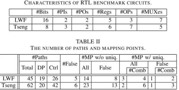
In the experiments, two RTL benchmark circuits, LWF and Tseng, were used to evaluate the proposed method. The circuit characteristics are shown in Table I. The number of RTL paths for each circuit is shown in Table II. In the table, columns “Total”, “DP” and “Ctrl” under column “#Paths” denote the total number of RTL paths and the numbers of paths in the data path and in the controller, respectively. Column
“#False” denotes the number of RTL false paths identified by the method proposed in [6] in the data path. The remaining columns shows the number of mapping points. Columns “#MP w/o uniq.” and “#MP w/ uniq.” denote the numbers of mapping
TABLE I
CHARACTERISTICS OFRTLBENCHMARK CIRCUITS.
#Bits #PIs #POs #Regs #OPs #MUXes
LWF 16 2 2 5 3 7
Tseng 8 3 2 6 7 5
TABLE II
THE NUMBER OF PATHS AND MAPPING POINTS.
#Paths #MP w/o uniq. #MP w/ uniq.
#False All False
Total DP Ctrl All False #Comb #Comb
LWF 45 19 26 5 14 8 3 4 1 2
Tseng 62 20 42 6 23 13 2 6 1 3
points without and with considering uniqueness of paths, respectively. Under these columns, columns “All” and “False” denote the numbers of mapping points for distinguishing any path from the others and for distinguishing false paths from the others, respectively. For the minimum mapping points using uniqueness of paths, there exists multiple combinations of mapping points. Under columns “All” and “False” of
“#MP w/ uniq.”, extra columns “#Comb” show the number of combinations. From this table, we can see that the number of mapping points which must be preserved were reduced very much by using uniqueness of paths. Furthermore, since only RTL false paths were considered, the number of mapping points were further reduced.
DesignCompiler ver. C-2009.06 (Synopsys) was used as a logic synthesis tool on SunFire X4100 (SunMicrosystems). By configuring the options of DesignCompiler, previous meth- ods, MIB-LS and MIP-LS, and proposed method, MPP-LS, were implemented. For MIB-LS, no constraint option of DesignCompiler was used. For MIP-LS, two configurations were implemented. One is just mapping each RTL module to gate level logic, i.e., it does not change interconnection between RTL modules. The other is implemented with the options “no boundary optimization” and “no autoungroup” of “compile ultra”. For MPP-LS, the option “set dont touch” was used to specify mapping points to be preserved. The former and latter are referred to as “MIP-LS” and “MIP′-LS”, respectively. Table III shows circuit characteristics of circuits synthesized from the benchmark circuits with MIB-LS, MIP- LS and MPP-LS, respectively. For LWF (column “LWF”), two timing constraints 40ns and 10ns (columns “40ns” and
“10ns”, respectively) were examined. Under each constraint, we performed MIB-LS, MPP-LS, MIP-LS and MIP′-LS. The circuit characteristics for these methods are shown in sub- columns “MIB”, “MPP”, “MIP” and “MIP′”, respectively. Rows “Area” and “Delay” denote the area in the number of gates equivalent and the clock period in nanosecond, respec- tively. For the proposed method, MPP-LS, the combination of mapping points which induces smallest area was used in this experiment. Sub-rows “Total”, “Data path” and “False” in row “#Paths” denote the numbers of total paths, paths in the data path and false paths in the data path at gate level, respectively. Note that the false paths were identified by mapping from RTL false paths using the path mapping method of [9]. We must mention that, for MPP and MIP,
199
TABLE III
CHARACTERISTICS OF SYNTHESIZED CIRCUITS.
Circuits LWF Tseng
Timing constraints 40ns 10ns 20ns 10ns
Synthesis methods MIB MPP MIP MIP′ MIB MPP MIP MIP′ MIB MPP MIP MIP′ MIB MPP MIP MIP′
Area 664 709 784 799 1,063 1,096 796 1,092 699 726 860 868 958 935 859 1,057
Delay 33.81 37.13 38.23 39.16 9.20 9.15 (30.37) 9.20 19.02 19.07 (20.86) 14.41 9.20 9.16 (20.86) 9.20 Total 29,098 46,838 47,446 47,446 138,262 111,510 59,086 123,878 33,932 33,940 36,152 34,258 74,344 68,036 36,152 65,658
# Paths Data path 11,072 13,420 14,404 12,076 52,684 38,924 14,404 38,492 30,736 30,680 32,490 30,868 68,204 64,088 32,490 61,820 False 3,296 4,272 4,574 3,798 18,328 14,952 4,574 14,824 1,072 15,906 15,966 15,996 3,568 14,574 16,404 12,542
%Ratio 29.8 31.8 31.8 31.5 34.8 38.4 31.8 38.5 3.5 51.8 49.1 51.8 5.2 22.7 50.5 20.3
!"
#$!!!"
%$!!!"
&$!!!" '$!!!" (!$!!!" (#$!!!" (%$!!!"
!)!" !)&" ()#" ()'" #)%" *)!" *)&" %)#" %)'" +)%" &)!" &)&" ,)#" ,)'" ')%" -)!" -)&" ./0 .11 ./12
!"#$%
&'#()*+,-
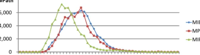
Fig. 2. The histogram of path length for LWF (10ns).
each bit-sliced signal line in the minimum set of RTL signal lines identifying the given RTL false paths was able to exactly map to its functionally equivalent gate level signal line. The last sub-row “%Ratio” in “#Paths” denotes the ratio of the number of false paths to that of paths in the data paths and it is referred to as false path identification ratio. The table also shows the synthesis results for Tseng as the similar manner as LWF. For Tseng, we used timing constraints 20ns and 10ns. The area of circuits synthesized by MPP-LS was almost the same as that by MIB-LS. For LWF with 10ns constraint and Tseng with both 20ns and 10ns constraints, MIP-LS was not able to meet the constraints (denoted with parenthesis in row
“Delay”). The false path identification ratio for MPP-LS was always best among feasible synthesis results (excluding results with timing violation) for any case.
Finally, the histogram of slacks of paths for each method with each timing constraint is shown to examine the impact on timing margin. Fig. 2 and 3 show LWF and Tseng with 10ns timing constraint, respectively. In the graphs, we omitted the results of MIP because it did not meet the timing constraiont. For each graph, x and y axes denote the number of paths and intervals of slack in nanosecond, respectively. For Tseng with 10ns, we can see that MIP’-LS has the largest impact on timing margin and the proposed method, MPP-LS, can alleviate the impact. For LWF with 10ns, the curves rose at almost the same point around 1.2ns. Therefore, we cannot observe any difference between them.
V. CONCLUSIONS
In this paper, a new synthesis method, called mapping point preserving-logic synthesis (MPP-LS), has been proposed to establish complete mapping between paths in an RTL circuit and its synthesized gate level circuit. Through the experiments, it has been shown that the proposed method can reduce hardware and timing overhead and improve propagability of
!"
#$!!!"
%$!!!"
&$!!!" '$!!!"
!(!" !(&" )(#" )('" #(%" *(!" *(&" %(#" %('" +(%" &(!" &(&" ,(#" ,('" '(%" -(!" -(&" ./0 .11 ./12
!"#$%
&'#()*+,-
Fig. 3. The histogram of path length for Tseng (10ns).
false path information through logic synthesis compared with the previous methods. Furthermore, the impact on timing margin has been examined and it is shown that the proposed method can reduce the impact.
ACKNOWLEDGMENTS
This work was supported in part by Japan Society for the Promotion of Science (JSPS) under Grants-in-Aid for Scientific Research (B) (No. 20300018).
REFERENCES
[1] K. T. Cheng and H. C. Chen, “Classification and identification of nonrobust untestable path delay faults,” IEEE Trans. on CAD, vol. 15, no. 8, pp. 845–853, Aug 1996.
[2] S. Kajihara, K. Kinoshita, I. Pomeranz, and S. Reddy, “A method for identifying robust dependent and functionally unsensitizable paths,” in Proc. of International Conference on VLSI Design, 1997, pp. 82–87. [3] S. M. Reddy, S. Kajihara, and I. Pomeranz, “An efficient method to
identify untestable path delay faults,” in Proc. of Asian Test Symposium, 2001, pp. 233–238.
[4] A. Krsti´c, S. T. Chakradhar, and K.-T. T. Cheng, “Testable path delay fault cover for sequential circuits,” in Proc. of European Design and Test Conference, 1996, pp. 220–226.
[5] R. Tekumalla and P. Menon, “Identifying redundant path delay faults in sequential circuits,” in Proc. of International Conference VLSI Design, 1996, pp. 406–411.
[6] Y. Yoshikawa, S. Ohtake, and H. Fujiwara, “False path identification using RTL information and its application to over-testing reduction for delay faults,” in Proc. of Asian Test Symposium, 2007, pp. 65–68. [7] Y. Yoshikawa, S. Ohtake, T. Inoue, and H. Fujiwara, “Fast false path
identification based on functional unsensitizability using RTL infor- mation,” in Proc. of 14th Asia and South Pacific Design Automation Conference 2009 (ASP-DAC’09), Jan 2009, pp. 660–665.
[8] S. Ohtake, N. Ikeda, M. Inoue, and H. Fujiwara, “A method of unsensitizable path identification using high level design information,” in Proc. of International conference on Design & Technology of Integrated Systems in nanoscale era (DTIS’10). To appear, Mar 2010.
[9] H. Iwata, S. Ohtake, and H. Fujiwara, “Enabling false path identification from RTL for reducing design and test futileness,” in Proc. of 5th IEEE International Symposium on Electronic Design, Test & Applications (DELTA’10), Jan 2010, pp. 20–25.
[10] S. Ravi, I. Ghosh, V. Boppana, and N. K. Jha, “Fault-diagnosis-based technique for establishing RTL and gate-level correspondences,” IEEE Trans. on CAD, vol. 20, no. 12, pp. 1414–1425, 2001.
200