Contents
Chapter 1: General introduction 1
1.1. Background 1
1.2. Overview of this thesis 3
1.3. Impurity doping 6
1.3.1. Principle of pn-control in organic semiconductors by doping 6
1.3.2. History of doping in organic semiconductors 8
1.3.3. The philosophy of doping in organic semiconductors in this thesis 10
1.3.4. Original points 12
1.3.5. Combination of doping and phase-separation 15
1.4. Basic principle of organic solar cells 18
1.4.1. Donor/acceptor sensitization 18 1.4.2. pn-heterojunction and pin-heterojunction
2.8. Measurements of the photovoltaic properties 38
2.8.1. Current-voltage (J-V) characteristics 38
2.8.2. Action spectra 42
2.8.3. Masking effect 43
2.9. References 45
Chapter 3: Conduction-type control of fullerene films from n - to p -type by molybdenum oxide doping 46
3.1. Introduction 47
3.2. Experiments 48
3.3. Results and discussion 49
3.3.1. Energy diagram of MoO3-doped C60 49
3.3.2. MoO3-doping mechanism 51
3.3.3. MoO3-doped Schottky-junction cell 53
3.4. Conclusion 58
3.5. References 59
Chapter 4: pn-homojunction formation in single fullerene films 61
4.1. Introduction 62
4.2. Experiments 63
4.3. Results and discussion 65
4.3.1. Photovoltaic properties of pn-homojunction C60 cells 65
4.3.2. Energetic structure of pn-homojunction C60 cells 69
4.4. Conclusion 71
4.5. References 72
Chapter 5: Invertible organic photovoltaic cells with heavily doped organic/metal ohmic contacts 74 5.1. Introduction 75 5.2. Experiments 76 5.3. Results and discussion
Chapter 7: pn-homojunction organic solar cells formed in phase-separated co-deposited
films 99
7.1. Introduction 100
7.2. Experiments 101
7.3. Results and discussion 102
7.3.1. Doping in phase-separated co-deposited films 102
7.3.2. pn-homojunction cells in phase-separated co-deposited film 105
7.3.3. Energy band diagram of the pn-homojunction cells in phase-separated co-deposited film 108
7.4. Conclusion 112
7.5. References 113
Chapter 8: General Conclusion 115
8.1. Summary of this thesis 115
8.2. Future prospects 117
List of publications and presentations 118
Acknowledgements 124
Chapter 1:
General introduction
1.1. Background
A huge amount of energy is consumed in Japan. However, without atomic energy,
ready for commercialization.2-3) The advantages of organic solar cells for commercialization can be summarized as follows.1)
(1) low-cost, (2) flexibility, (3) light weight, (4) roll-to-roll production, (5) printable, (6) high efficiency under low-intensity light, and (7) transparent and colorful designs.
In this thesis, the author describes fundamental research carried out into small-molecule organic solar cells. The author developed a new-type of organic solar cell based on a concept used in inorganic solar cells.
1.2. Overview of this thesis
In inorganic solar cells, pn-homojunctions in single inorganic semiconductors have often been utilized. In this thesis, organic solar cells based on this concept used in inorganic semiconductors are proposed. The author developed pn-homojunction organic solar cells, that is, pn-homojunctions formed in single uniform films of organic semiconductor by impurity doping.
Previously, various impurity-doping techniques for organic semiconductors have been performed. However, the doping of organic semiconductors has mainly been in the concentration range of the order of a few %.
ppm-level doping technique, and the photovoltaic measurements, are described.
In Chapter 3, pn-control in a C60 film is described. The author chose C60 as a test material because most recent solar cells contain C60.4-20) Since C60 films behave like n-type semiconductors, the author tried first of all to change the conduction type from n- to p-type by doping. It was confirmed that molybdenum oxide (MoO3) behaved as an acceptor. As far as the author knows, this is the first report on the formation of p-type C60. Based on these results, general pn-control in other various organic semiconductors was performed.19-25)
In Chapter 4, the formation of pn-homojunctions in single C60 films by doping is described. The position of the junction was intentionally controlled by changing the thicknesses of the MoO3 and Ca doped regions. This mechanism for the formation of pn-homojunctions is based on the differences in EF caused by the controlled doping, and offers a potential method for the design and creation of a built-in potential in organic solar cells.
In Chapter 5, invertible H2Pc/C60 heterojunction cells with heavily doped organic/metal contacts are described. This is an application of the doping technique developed in Chapters 3 and 4. Ohmic contacts for metal electrodes were formed by using heavily p+- or n+-doped organic semiconductor layers. This is a similar concept to the formation of ohmic contacts in inorganic semiconductors.26-29) This heavy doping technique was used to fabricate the cells in Chapter 7.
In Chapter 6, the fabrication of pn-homojunctions in co-deposited films consisting of C60 and H2Pc is described.
In Chapter 7, the formation of pn-homojunctions in phase-separated co-deposited films of an organic semiconductor is described. The carrier transport in the
film was improved by introducing a co-evaporant on to the heated substrate during film growth to produce phase-separated co-deposited films (Chapter 1.5). Since the conductivity (σ) is the product of the mobility (µ) and the carrier concentration (n), i.e., σ = enµ [e; electron charge], the cell resistance (σ-1) can be reduced by increasing both n, by means of doping, and µ, by means of introducing the co-evaporant. Thus, the author attempted to combine doping with the introduction of a co-evaporant. This technique permitted fabrication of very thick cells up to 0.5 µm thick with very long minority carrier (electron) diffusion lengths of 250 nm. Previously, the doping technique has been used only in the carrier transport layers of organic solar cells.26-27, 30)
However, in this study, the doping technique was applied directly to the photocurrent generation layer. The concept of majority and minority carriers in organic solar cells is introduced for the first time.
1.3. Impurity doping
1.3.1. Principle of pn-control in organic semiconductors by doping
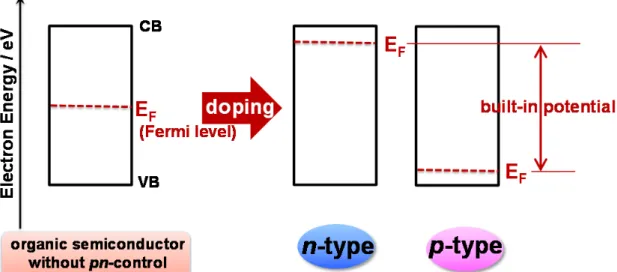
Precise pn-control by impurity doping is vital for intentionally creating a built-in potential in semiconductors (Fig. 1.3.1).31) For undoped semiconductors, the Fermi level (EF) is located at the center of the bandgap. By doping with donor impurities, EF shifts in the negative direction and arrives near the lower edge of the conduction band (n-type). By doping with acceptor impurities, EF shifts in the positive direction and arrives near the upper edge of the valence band (p-type). Thus, a potential difference is created between then- and p-type semiconductors (Fig. 1.3.1). With the p- and n-type semiconductors in contact with each other, a pn-homojunction is formed.32) This is the complete pn-control technique and has long been established for inorganic semiconductors. However, for organic semiconductors, there are only a few examples33-35) of complete pn-control and the formation of pn-homojunctions.
Figure 1.3.2 shows the pn-control mechanism for organic semiconductors. In the case of p-type doping, the energy level of the LUMO of an acceptor is lower than that of the HOMO of the organic semiconductor. So, due to electron transfer, under dark conditions, the acceptor molecule is negatively charged and the organic semiconductor is positively charged. As a result, the organic semiconductor becomes p-type. In the case of n-type doping, the energy level of the HOMO of the donor is higher than that of the LUMO of the organic semiconductor. So, the donor molecule is positively charged and the organic semiconductor is negatively charged. As a result, the organic semiconductor becomes n-type. When a single organic semiconductor is used for both the n- and p-type doping, one can regard that complete pn-control has been achieved.
Fig. 1.3.1 Concept of the formation of a built-in potential by impurity doping.
Fig. 1.3.2 pn-control for organic semiconductors.
1.3.2. History of doping in organic semiconductors
The real nature of organic semiconductors has been hidden for a long time due to uncontrolled impurities, typically oxygen from the ambient. Since oxygen acts as an acceptor impurity, most organic semiconductors, such as phthalocyanines, show p-type characteristics. Researchers believed that such p-type characteristics are an inherent property of organic semiconductors. However, Martin36) and Tada37) reported that phthalocyanines showed n-type characteristics when an ultra-high vacuum was used to completely eliminate oxygen during the film deposition process and the measurements. These results suggest the possibility of pn-control for organic semiconductors by intentional doping.
Figure 1.3.3 shows the dopants for organic semiconductors. Before 2000, the dopants for impurity doping organic semiconductors were limited to just a few. For acceptors, halogen vapors such as I2 and Br2 were used.38-39) For example, a pn-homojunction was formed by a controlled change in the conduction type from n- to p-type by doping perylene pigment with Br2.40) For donors, alkali metals such as Na and Ca have been used. However, these dopants are easily oxidized in air.
Recently, Tokito41) and Matsushima42) reported metal oxides such as molybdenum oxide (MoO3) and vanadium oxide (V2O5) as hole injection layers for organic electroluminescence (EL) devices. In the present work, the author attempted using these oxides as acceptor dopants for organic solar cells. On the other hand, Yang has reported carbonates of alkali metals such as cesium carbonate (Cs2CO3) for the electron injection layers for organic EL devices.43-44) Ishiyama20, 22-23) used Cs2CO3 as a donor dopant for organic solar cells. These dopants are relatively stable in air. On the other hand, Leo45-46), Harada33,35), and Kahn34) reported organic dopants such as
2,3,5,6-Tetrafluoro-7,7,8,8-tetracyanoquinodimethane (F4-TCNQ), Ru-complex, and Co-complex, respectively. Harada et al. fabricated pn-homojunctions in Zinc phthalocyanine and pentacene films using these organic dopants.33)
Fig. 1.3.3 Acceptor (left) and donor (right) dopants for organic semiconductors.
1.3.3. The philosophy of doping in organic semiconductors in this thesis Previously, the doping of organic semiconductors has been performed in the concentration range of the order of a few %. The author believes that a doping technique with very low-concentrations of the order of ppm should be developed for the following reasons.
(i) ppm-level doping is performed in the field of inorganic semiconductors.
(ii) In the case of doping of the order of a few %, side effects, such as decreases in carrier mobility due to scattering by dopant molecules and decreases in carrier life-time due to recombination with ionized dopants, are expected. These side effects easily degrade the performance of solar cells.
(iii) When the doping is directly applied to the photocurrent generation layer, the side effects due to doping need to be minimized in order to obtain a high conversion efficiency. Thus, the ppm-doping technique is imperative.
Doping at the ppm-level is highly challenging. To realize ppm-level doping, the author utilized the following techniques.
(1) Highly purified organic semiconductors.
For ppm-level doping, highly purified organic semiconductors should be used. In this thesis, ‘seven-nines’ (7N; 99.99999%) purified organic semiconductors (fullerene: C60, metal-free phthalocyanine: H2Pc) were used (Chapter 2.1).21)
(2) Highly precise control of the deposition rate of the dopants.
In this thesis, the author utilized a computer monitoring system linked with a quartz crystal microbalance (QCM) and developed expertise in a ppm-doping technique based on co-evaporation (Chapter 2.6).
(3) No exposure to air.
The cells fabricated during this study were prevented from exposure to air at any time during both fabrication and measurement. The position of EF in organic semiconductor films is known to be very sensitive to oxygen.36-37, 47) Therefore, during both fabrication and measurements, the cells were prevented from exposure to air by using a glove box containing a built-in evaporation chamber and a Kelvin probe (Chapter 2.2).
1.3.4. Original points
Based on the philosophy mentioned in section 1.3.3., the author achieved the following two breakthroughs with doping.
(1) Formation of p-type C60.
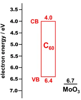
C60 is difficult to oxidize. Since the HOMO level of C60 is extremely deep (6.4 eV) (Fig. 1.3.4), previously, no one had succeeded in oxidizing C60 and forming p-type C60. The author undertook this challenge. The author discovered that MoO3 had an extremely deep work function (6.7 eV) (Fig. 1.3.4) if it had been prevented from exposure to air. Since the work function of a film easily shifts in the negative direction when exposed to air, air free conditions using a glove box with a built-in evaporation chamber and a Kelvin probe were vital for this discovery. The author performed experiments on doping C60 with MoO3 and observed a positive shift of the Fermi level in the C60 film. This was the first breakthrough in this work. All the pn-homojunction organic solar cells fabricated for the work described in this thesis were based on this result.
(2) Organic solar cells with inorganic-like pn-homojunctions
Impurity doping of the photocurrent generation layer in an organic solar cell has never previously been performed. The author attempted to directly dope the photocurrent generation layer of an organic solar cell for the first time and thereby fabricate pn-homojunction organic solar cells. Majority and minority carriers were clearly distinguished after doping. The author demonstrated that the pn-homojunction organic solar cells presented in this thesis operate by essentially the same mechanism as pn-homojunction inorganic solar cells.
Figure 1.3.5 shows a typical example of the energy band structure of an
inorganic pn-homojunction.48) By impurity doping, a pn-homojunction is formed in the single inorganic semiconductor. In the p-layer, electrons and holes act as minority and majority carriers, respectively. The photocarrier generation region consists of a depletion layer (shaded red) and a minority carrier diffusion region of length L (shaded blue). Even in the region without a built-in potential (blue region), photogenerated electrons can be extracted to the n-type region due to the large minority carrier diffusion length (L). On the other hand, the high concentration of holes means these can easily be extracted to the opposite electrode. A long minority carrier diffusion length is a key factor for photocurrent generation.
In Chapter 7, the fabrication of an organic pn-homojunction with a similar operating mechanism to that of an inorganic pn-homojunction is reported. This is the first example of an organic solar cell with an inorganic-like pn-homojunction.
Fig. 1.3.4 Energy diagram of C60 (left) and work function of MoO3 (right).
Fig. 1.3.5 Energy band structure of inorganic pn-homojunctionsolar cell.
1.3.5. Combination of doping and phase-separation
The minority carrier diffusion length (L) is expressed by the equation (Eq. 1.1). L = μkTe τ /
and holes increases their mobility. Since there is a built-in potential due to the pn-homojunction in the C60:H2Pc film, the e- and h+ photocarriers are expected to move in opposite directions (Fig. 1.3.8, center). This result is described in Chapter 7.
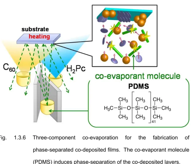
Fig. 1.3.6 Three-component co-evaporation for the fabrication of phase-separated co-deposited films. The co-evaporant molecule (PDMS) induces phase-separation of the co-deposited layers.
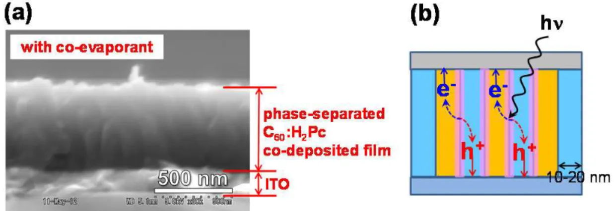
Fig. 1.3.7 (a) Cross sectional SEM image of a phase-separated C60:H2Pc co-deposited film (500 nm) on an ITO glass substrate which was mechanically cut using a diamond glass cutter. (b) An ideal nanostructure comprising a vertical superlattice structure of C60
(brown regions) and H2Pc (blue regions).
Fig. 1.3.8 Combination of doping and phase-separation. A pn-homojunction is formed in the phase-separated co-deposited film.
1.4. Basic principle of organic solar cells
1.4.1. Donor/acceptor sensitizationDonor/acceptor sensitization is essential for organic solar cells in order to obtain a significant amount of photocurrent.5, 19, 22-23, 50)
The photocarrier generation process in organic semiconductors is strongly affected by their small relative permittivity (ε). ε is contained in the denominator of the equation of Coulomb's law (Eq. 1.2). Therefore, the smaller ε is, the greater the attractive force between the negative and positive charges.
F = 1
4πεε q q
r
excitons can easily dissociate to free carriers (Fig. 1.4.2(b), left). Thus, a photocurrent with a significant magnitude can be generated.
Fig. 1.4.1 (a) Wannier exciton in inorganic semiconductor, (b) Frenkel exciton in organic semiconductor.
Fig. 1.4.2 (a) Free carriers are rarely generated due to the relaxation of Frenkel excitons. (b) Free carriers are easily generated from a charge transfer (CT) exciton.
+
1 nm Inorganic semiconductor
ε≒11.9 (Si)
Dissociate easily into free carriers
(a)
Radius of exciton : 0.25 nm
Organic semiconductor ε≒4 (C60)
(b)
+
Radius of exciton : 4.5 nm
-
-
-
Dissociation hardly occurs
+ -
+ -
Electron energy / eV
3.0 4.0 5.0 6.0 7.0 Frenkel exciton
Chage transfer (CT) exciton
LUMO LUMO
HOMO
HOMO free carrier
e-and h+
free carrier e-and h+
LUMO
HOMO relaxation photo
-excitation molecule
Molecule A
hν
(a)
(b)
Molecule B
1.4.2. pn-heterojunction and pin-heterojunction
Donor/acceptor sensitization occurs at the pn-heterojunction in a two layer cell (Fig 1.4.3(a)).32) Unfortunately, since the distance excitons can move is only a few nm, only those within about 10 nm of the heterojunction can generate free carriers by reaching the donor/acceptor junction (pn-heterojunction).48, 55) Thus, thick pn-heterojunction cells have dead-layers which can absorb light, but in which photocurrent cannot be generated. Furthermore, 10 nm thick cells cannot absorb all the solar light, so, in order to utilize all the solar light, a different approach is needed.
To overcome this problem, the pin-heterojunction has been introduced (Fig. 1.4.3).56-58) An i-layer is a co-deposited layer of a donor/acceptor organic semiconductor. Thus, the whole layer becomes active for photocurrent generation because donor and acceptor molecular sites exist throughout the film. If a sufficiently thick co-deposited i-layer could be used, it would absorb all the solar light. The co-deposited layer in this pin-heterojunction cell can be regarded as a blended-junction, or so-called bulk heterojunction. This concept is essential for fabricating the latest types of organic solar cells.5-14, 16-17, 27, 50)
Fig. 1.4.3 (a) pn-heterojunction cell. Photocurrent is generated only within about 10 nm of the heterojunction. (b) pin-heterojunction cell. Photocurrent is generated in the whole co-deposited i-layer.
Donor/acceptor
heterojunction
-
+
h + e -
-
+
photocurrent
generation layer
(≒10 nm) dead layer
hν
hν
hν
n-type
layer
p-type
layer
(a)
(b)
photocurrent generation layer
(whole co-deposited i-layer)
-
+
h + e -
-
+
h + e -
1.5. Aims of this thesis
The main aims of this thesis are as follows.
(1) Establishment of complete pn-control for a typical organic semiconductor (C60). The author attempted the complete pn-control in fullerene (C60) because most recent organic solar cells contain C60. Since its HOMO level is extremely deep, C60 is difficult to oxidize. Therefore, the author undertook the challenge of finding an acceptor dopant that could extract electrons from C60. After discovering a suitable candidate, the author performed ppm-doping using this dopant and attempted fabricating pn-homojunctions in C60 films.
(2) Demonstration of organic solar cells with inorganic-like pn-homojunctions.
Previously, in organic solar cells, impurity doping of a photocurrent generation layer has never been performed. The author attempted to directly dope the photocurrent generation layer of an organic solar cell for the first time and to fabricate pn-homojunction organic solar cells with ppm-level doping. The author’s expectations were that inorganic-like thick organic solar cells could be fabricated by the formation of an inorganic-like pn-homojunction.
1.6. References
1) Research by New Energy and Industrial Technology Development Organization (NEDO).
2) M. A. Green, K. Emery, Y. Hishikawa, W. Warta, and E. D. Dunlop, Prog. Photovolt: Res.Appl, 22, 1 (2014).
3) R. Service, Science, 332, 293 (2011).
4) N. S. Sariciftci, D. Braun, C. Zhang, V. I. Srdanov, A. J. Heeger, G. Stucky, F. Wudl, Appl. Phys. Lett., 62, 585 (1993).
5) J. Sakai, T. Taima, and K. Saito, Org. Electron., 9, 582 (2008).
6) T. Taima, M. Chikamatsu, Y. Yoshida, K. Saito, and K. Yase, Appl. Phys. Lett., 85, 6412 (2004).
7) J. Xue, B. P. Rand, S. Uchida, and S. R. Forrest, Adv. Mater., 17, 66 (2005). 8) K. Suemori, T. Miyata, M. Yokoyama, and M. Hiramoto, Appl. Phys. Lett., 86,
063509 (2005).
9) T. Kaji, M. Zhang, S. Nakao, K. Iketaki, K. Yokoyama, C. W. Tang, and M. Hiramoto, Adv. Mater., 23, 3320 (2011).
10) Y. Zhou, T. Taima, T. Miyadera, T. Yamanari, M. Kitamura, K. Nakatsu, and Y. Yoshida, Appl. Phys. Lett., 100, 233302 (2012).
11) D. Wynands, M. Levichkova, K. Leo, C. Uhrich, G. Schwartz, D. Hildebrandt, M. Pfeiffer, and M. Riede, Appl. Phys. Lett., 97, 073503 (2010).
12) M. Hiramoto, K. Kitada, K. Iketaki, and T. Kaji, Appl. Phys. Lett., 98, 023302 (2011).
13) J. Meiss, F. Holzmueller, R. Gresser, K. Leo and M. Riede, Appl. Phys. Lett., 99, 193307 (2011).
14) W. Chen, X. Qiao, J. Yang, B. Yu, and D. Yan, Appl. Phys. Lett., 100, 133302 (2012).
15) K. Schulze, C. Uhrich, R. Schuppel, K. Leo, M. Pfeiffer, E. Brier, E. Reinold, and P. Bauerle, Adv. Mater., 18, 2872 (2006).
16) D. Wynands, M. Levichkova, M. Riede, M. Pfeiffer, P. Baeuerle, R. Rentenberger, P. Denner, and K. Leo, J. Appl. Phys., 107, 014517 (2010).
17) V. Steinmann, N. M. Kronenberg, M. R. Lenze, S. M. Graf, D. Hertel, H. Burckstummer, F. Wurthner, and K. Meerholz, Appl. Phys. Lett., 99, 193306 (2011). 18) T. Taima, J. Sakai, T. Yamanari and K. Saito, Jpn. J. Appl. Phys., 45, 995 (2006). 19) N. Ishiyama, M. kubo, T. Kaji, and M. Hiramoto, Appl. Phys. Lett., 99, 133301
(2011).
20) N. Ishiyama, M. kubo, T. Kaji, and M. Hiramoto, Appl. Phys. Lett., 101, 233303 (2012).
21) M. Hiramoto, M. Kubo, Y. Shinmura, N. Ishiyama, T. Kaji, K. Sakai, T. Ohno, and M. Izaki, Electronics, 3, 351-380 (2014).
22) N. Ishiyama, M. kubo, T. Kaji, and M. Hiramoto, Org. Electron., 14, 1793 (2013). 23) N. Ishiyama, T. Yoshioka, T. Kaji, and M. Hiramoto, Appl. Phys. Express, 6, 012301
(2013).
24) Y. Shinmura, M. Kubo, N. Ishiyama, T. Kaji, and M. Hiramoto, AIP Advances, 2, 032145 (2012).
25) Y. Shinmura, M. Kubo, T. Kaji, and M. Hiramoto, Jpn. J. Appl. Phys., 52, 04CR12 (2013).
26) K. Walzer, B. Maenning, M. Pfeiffer, and K. Leo, Chem. Rev., 107, 1233 (2007).
27) C. Falkenberg, C. Uhrich, S. Olthof, B. Maemming, M. K. Riede, and K. Leo, J. Appl. Phys., 104, 034506 (2008).
28) J. C. deMello, N. Tessler, S. C. Graham, and R. H. Friend, Phys. Rev. B, 57, 12951 (1998).
29) M. Hiramoto, A. Tomioka, K. Suemori, and M. Yokoyama, Appl. Phys. Lett., 85, 1852 (2004).
30) R. Timmreck, S. Olthof, K. Leo, and M. K. Riede, J. Appl. Phys., 108, 033108 (2010).
31) W. E. Spear, and P. E. Lecomber, Solid State Commun., 17, 1193 (1975). 32) C. W. Tang, Appl. Phys. Lett., 48, 183 (1983).
33) K. Harada, A. G. Werner, M. Pfeiffer, C. J. Bloom, C. M. Elliott, and K. Leo, Phys. Rev. Lett., 94, 036601 (2005).
34) C. K. Chan, W. Zhao, S. Barlow, S. Marder, amd A. Kahn, Organic Electronics, 9, 575 (2008).
35) K. Harada, M. Riede, and K. Leo, Phys. Rev. B, 77, 195212 (2008). 36) M. Martin, J. –J. Andre, and J. Simon, J. Appl. Phys., 54, 2792 (1983).
37) H. Tada, H. Touda, M. Takeda, and K. Matsushige, Appl. Phys. Lett., 76, 873 (2000).
38) H. Akamatsu, H. Inokuchi, and Y. Matsunaga, Nature, 173, 168 (1954).
39) M. Hiramoto, K. Ihara, H. Fukusumi, and M. Yokoyama, J. Appl. Phys., 78, 7153 (1995).
40) M. Hiramoto, K. Ihara, and M. Yokoyama, Jpn. J. Appl. Phys., 34, 3803 (1995). 41) S. Tokito, K. Noda, and Y. Taga, J. Phys. D: Appl. Phys., 29, 2750 (1996).
42) T. Matsushima, Y. Kinoshita, and H. Murata, Appl. Phys. Lett., 91, 253504 (2007).
43) H. –H. Liao, L. –M. Chen, Z. Xu, G. Li, and Y. Yang, Appl. Phys. Lett., 92, 173303 (2008).
44) S. Hamwi, T. Riedl, and W. Kowalsky, Appl. Phys. Lett., 99, 053301 (2011). 45) J. S. Huang, M. Pfeiffer, A. Werner, J. Blochwitz, K. Leo, and S. Y. Liu, Appl. Phys.
Lett., 80, 139 (2002).
46) J. Blochwitz, M. Pfeiffer, T. Fritz, and K. Leo, Appl. Phys. Lett., 73, 729 (1998). 47) Y. Tanaka, K. Kanai, Y. Ouchi, and K. Seki, Chem. Phys. Let., 441, 63 (2007). 48) M. Yamaguchi, IEICE, 93, 212 (2010).
49) M. Hiramoto, T. Yamagata, M. Danno, K. Suemori, Y. Matsumura, and M. Yokoyama, Appl. Phys. Lett., 88, 213105 (2006).
50) J. Sakai, T. Taima, T. Yamanari, and K. Saito, Sol. Energy Mater. Sol. Cells, 93, 1149 (2009).
51) A. F. Hebard, R. C. Hadon, R. M. Fleming, and A. R. Kortan, Appl. Phys. Lett., 59, 2109 (1991).
52) M. A. Abkowiz and A. I. Lakatos, J. Chem. Phys., 57, 5033 (1972). 53) G. A. Chamberlain, Solar Cells, 8, 47 (1983).
54) H. Spanggaard and F. C. Krebs, Sol. Energy Mater. Sol. Cells, 83, 125 (2004). 55) P. Peumans, A. Yakimov, and S. R. Forrest, 93, 3693 (2003).
56) M. Hiramoto, H. Fujiwara, and M. Yokoyama, Appl. Phys. Lett., 58, 1062 (1991). 57) M. Hiramoto, H. Fujiwara, and M. Yokoyama, J. Appl. Phys., 72, 3781 (1992). 58) G. Yu, J. Gao, J. C. Hummelen, F. Wudl, and A. J. Heeger, Science, 270, 1789
(1995).
Chapter 2:
Experiments
2.1. Purification of materials
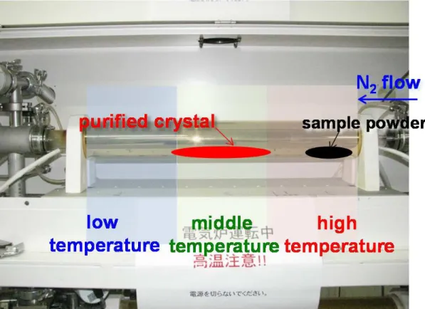
Highly purified organic semiconductors were used for ppm-level doping. The C60 (Frontier Carbon, nanom purple TL) single crystal sample was formed by sublimation in apparatus with a N2 flow at a pressure of 1 atm (Fig. 2.1).1) The apparatus had three temperature zones; high, middle, and low zones set at temperatures of 745oC, 580oC, and 310oC, respectively. C60 powder was placed in the high temperature zone and purified crystals were formed in the middle temperature zone. Fig. 2.2(a) shows the purified C60
crystals which range in size from 1 to 2 mm. The purity of the crystals was determined to be in the ‘seven-nines’ range (7N; 99.99999%) by secondary ion mass spectroscopy.2-4)
The H2Pc (Dainippon Ink and Chemicals, Inc., Fastogen Blue EP-101) sample was purified in a N2 flow at a pressure of 0.1 atm in order to avoid decomposition. The temperatures of the high, middle, and low zones were 480oC, 290oC, and 270oC, respectively. H2Pc powder was placed in the high temperature zone and purified crystals were formed in the middle temperature zone. Fig. 2.2(b) shows the purified H2Pc crystals which are needle shaped and about 10 mm long. The purity of the H2Pc crystals was also determined to be in the ‘seven-nines’ range (7N; 99.99999%) by Hall effect measurements.5)
MoO3 (Alfa Aeser, 99.9995%), V2O5
Fig. 2.1 Photograph of apparatus used for sublimation of single crystal material.
Fig. 2.2 Purified crystals of (a) C60 and (b) H2Pc.
2.2. Glove box with built-in evaporation chamber
The electrical properties of organic semiconductors are strongly influenced by oxygen and water adsorbed from the atmosphere. For example, measurements of the Fermi level (EF) in an organic film using a Kelvin probe are very sensitive to adsorbed oxygen, so reproducible results cannot be obtained in air. Therefore, in this study, a glove box (Miwa, DBO-1.5) containing a built-in evaporation chamber (ULVAC, VTS-350M/ERH) and a Kelvin probe was used (Fig. 2.3). The glove box was purged by N2 gas, in which the concentrations of H2O and O2 were kept below 0.5 and 0.1 ppm, respectively. For the photovoltaic measurements the cells were prevented from being exposed to air by placing them in a sample container with a quartz window inside the glove box (Fig. 2.10). Thus, at any time during both fabrication and measurement the cells were prevented from exposure to air.
Fig. 2.3 Glove box with built-in evaporation chamber. Kelvin probe is also set in the glove box.
2.3. Kelvin probe measurements
The Fermi levels (EF) of doped and undoped organic semiconductor films with thicknesses of 100 or 200 nm were measured using the Kelvin vibrating capacitor apparatus (Riken-Keiki, FAC-1) inside the glove box and prevented from exposure to air (Fig. 2.4).6-8) Fig. 2.5 shows a schematic diagram illustrating the Kelvin probe measurement method. A capacitor (C) is formed between the vibrating Au plate and the sample film on an indium tin oxide (ITO) substrate. The charge (Q) induced by the electrodes which have a contact potential difference of ΦAu-ΦS is expressed by the following equation (Eq. 2.1).
Q = C(ΦAu-ΦS) (2.1)
Here, ΦAu and ΦS represent the work functions of the Au and the sample film, respectively.
On the application of a voltage (VEX), Q becomes (Eq. 2.2).
Q = C(ΦAu-ΦS-VEX) (2.2) Here, a current (ΔQ = dQ/dt) is generated due to the vibration of the Au plate (Eq. 2.3).
ΔQ = ΔC(ΦAu-ΦS-VEX) (2.3) Thus, ΦS can be determined from the value of VEX required to make ΔQ=0 and the value of ΦAu (5.1 eV) measured by atmospheric X-ray photoelectron spectroscopy (Eq. 2.4).9)
ΦS = ΦAu-VEX(ΔQ = 0) (2.4)
Fig. 2.4 Photograph of Kelvin vibrating capacitor apparatus.
Fig. 2.5 Schematic diagram of Kelvin vibrating capacitor method.
+
+
+
+
-
-
-
-
Au plate
capacitance
C
vibration
samples
ammeter
V
EX2.4. Energy band mapping of doped junctions
The band-bending in the depletion layer formed at the junction was mapped to measure the thickness dependence of the work function using the Kelvin probe.10) Figure 2.6 shows the concept of energy mapping using the Kelvin probe. As an example, the energy band diagram of the Schottky junction between an ITO substrate and a p-type film is shown. First the Fermi levels (EF) of the ITO and the p-type semiconductor are aligned (broken line), causing the energy bands to bend. The vacuum level (EV) shown by the dotted curve bends following the conduction and valence bands. Thus, the work function measured by the Kelvin probe (double-headed red arrows) increases with increasing film thickness. As a result, the band-bending of a doped film can be mapped by repeated film depositions and measurements of the work function. This method can also be applied to a pn-homojunction in an organic film (see Chapter 7).
Fig. 2.6 Energy mapping concept using a Kelvin probe. An example of a Schottky junction between ITO and a p-type doped semiconductor film is shown.
ITO p-type doped film
4.7 eV 0 eV
5 nm 20 nm 50 nm
Fermi level : E
FCB
VB
work function = EV - EF (measured by kelvin probe)
ITO
ITO ITO ITO
vacuum level : E
V2.5. Multi-component co-evaporation
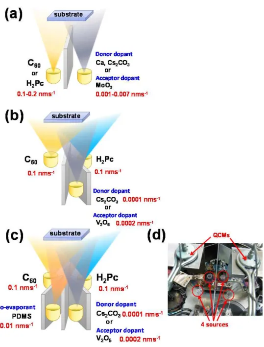
Doping was performed by multi-component co-evaporation techniques (Fig. 2.7). Fig. 2.7(a) shows the two-component co-evaporation technique which was used in making the samples described in Chapters 3, 4, and 5. In these cases, single organic semiconductor films were doped, either with the acceptor dopant, MoO3, or with the donor dopants, Ca or Cs2CO3. The doping concentrations were from 3300 to 50000 ppm in volume.
Fig. 2.7(b) shows the three-component co-evaporation technique, which was used for making the samples presented in Chapter 6. Co-deposited films of C60 and H2Pc were doped. V2O5 and Cs2CO3 were used as the acceptor and donor dopants, respectively, and the doping concentrations were between 1000 ppm and 500 ppm in volume.
Fig. 2.7(c), (d) show the four-component co-evaporation technique used to make the samples described in Chapter 7. Co-deposited films (C60:H2Pc), phase-separated by the introduction of a co-evaporant molecule, were doped with V2O5
and Cs2CO3 with doping concentrations between 1000 ppm and 500 ppm in volume. Polydimethylsiloxane (PDMS41, CH3[(CH3)2SiO]nSi(CH3)3) (Shin-Etsu Silicones, KF96-50cs, 100%) was used for the co-evaporant (Chapters 1.3.5. and 7).11)
Fig. 2.7 Multi-component co-evaporation. (a) Two-component co-evaporation, (b) three-component co-evaporation, and (c) four-component co-evaporation. (d) Photograph of four-component co-evaporation setup in the vacuum chamber. Four quartz crystal microbalances (QCMs) which can independently monitor four different materials from four different sources were used.
2.6. ppm-level doping technique
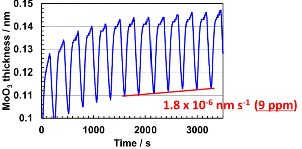
In order to perform doping at the ppm-level, a computer monitoring system (ULVAC, CRTM-6000G/Depoview) linked with a quartz crystal microbalance (QCM) was used. Fig. 2.8 shows the typical monitored thickness-time dependence. The cyclic fluctuations are due to temperature fluctuations in the QCM cooling water caused by the on/off switching of the chiller. A reproducible increase in the baseline (red line) was observed. In this case, a deposition rate of 1.8 x 10⁻⁶ nm s-1 was obtained from the slope of the baseline. On the other hand, the deposition rate of the host organic semiconductor (C60:H2Pc) was 0.2 nm s-1. Therefore, a doping concentration of 9 ppm in volume can be obtained (1.8 x 10⁻⁶ / 0.2 = 9 x 10⁻⁶).
A lot of knowledge and expertise is required to perform ppm-doping. Without the computer monitoring system, controlling the doping concentration to the ppm-level is impossible due to the cyclic fluctuations shown in Fig. 2.8. In the case of 9 ppm doping (Fig 2.8), it usually took from about 2 to 6 hours to adjust the extremely slow dopant deposition rate of 1.8 x 10⁻⁶ nm s-1. The doping for co-deposited films and phase-separated co-deposited films was performed by three-component and four-component co-evaporation. Therefore, simultaneous control of the deposition rates of two different host organic semiconductors, the dopant, and the co-evaporant was needed. The ppm-doping technique combined with multi-component co-evaporation has never been performed before.
Fig. 2.8 Typical thickness-time relationship shown on the PC monitor. An example of 9 ppm-doping with MoO3 is shown.
0.1
0.11
0.12
0.13
0.14
0.15
0 1000 2000 3000
MoO3thickness / nm
Time / s
1.8 x 10
-6nm s
-1(9 ppm)
2.7. Substrate heating
Fig. 2.9 shows a photograph of the apparatus used to heat the substrate (EpiTech, custom-made). In the case of four-component co-evaporation using the co-evaporant (PDMS41) (Chapter 1.3.5 and 7), the substrate temperature during deposition was raised to 70oC in order to fabricate the phase-separated and crystallized co-deposited films and re-evaporate the co-evaporant. ppm-doping on to a heated substrate has never been performed before.
Fig. 2.9 Photograph of apparatus for substrate heating.
2.8. Measurements of the photovoltaic properties
2.8.1. Current-voltage (J-V) characteristicsThe photovoltaic properties were also measured without exposure to air by setting the cells into a sample container with a quartz glass window (EpiTech, custom-made) (Fig. 2.10) inside the glove box. The area of the light incident on the cells was precisely limited to 0.04 cm2 by using a metal mask with 2 mm x 2 mm apertures (Fig. 2.11). A turbo-molecular pump was used to maintain a pressure of 10-5 Pa during the measurements. The current-voltage (J-V) characteristics were measured by irradiating the cells with a simulated solar light source (USHIO INC., MS-110AAA)
conversion efficiency (η). The maximum FF value of 1.0 corresponds to the rectangular J-V characteristic in the first quadrant shown by the broken line (Fig. 2.13). So, the conversion efficiency (η) becomes larger as the J-V curve of the photocurrent (red curve, Fig. 2.13) approaches a rectangular shape (broken line, Fig. 2.13), i.e., FF approaches 1.0.
Fig. 2.10 Sample container with a quartz glass window for photovoltaic measurements under vacuum.
Fig. 2.11 Photograph of a cell and the metal mask with apertures used to restrict the area of irradiation.
Fig. 2.12 (a) J-V characteristics measurement. (b) Measured J-V curves on PC monitor.
Fig. 2.13 Typical J-V characteristics in the dark (blue curve) and under light irradiation (red curve).
Current density (J) / mA cm-2
Voltage (V) / V
J
MAXV
MAX0
J
scV
oc0
2.8.2. Action spectra
The action spectra of the short-circuit photocurrent density were measured by irradiating with monochromatic light from a Xe-lamp passed through a monochromator (Shimadzu, SPG-3ST) (Fig. 2.14). The external quantum efficiency (EQE) was determined by the ratio of the number of carriers collected under the short-circuit condition to the number of photons irradiating the cell, measured using a silicon photodiode (Hamamatsu Photonics, S1337-66BQ). Typical action spectra, i.e., the spectral dependence of the EQE of the short-circuit photocurrent, are shown in Fig. 2.15(c) and (d). The maximum EQE value of 100% means that 100 photons are converted to 100 electrons in the cell.
Fig. 2.14 System for action spectra measurements.
2.8.3. Masking effect
The location of the region where photocurrent is generated with respect to the electrode irradiated with light can be determined based on the shape of the action spectra.
If the action spectrum appears in a wavelength region with a large absorption coefficient in the cell (Fig. 2.15(c)), the photocurrent is generated close to the electrode being irradiated (Fig. 2.15(a), blue shade). On the other hand, when the action spectrum appears around the edge of the absorption spectrum of the cell (Fig. 2.15(d)), the photocurrent is not generated close to the electrode, but on the side of the cell away from the electrode (Fig. 2.15(b), red shade). In this case, there is a dead region close to the irradiated electrode acting as a mask which absorbs incident light and does not generate photocurrent. The photocurrent is generated by light penetrating deep into the cell. This is the so-called “masking effect”. This proves that the photocurrent is generated in a region located on the opposite side of the cell with respect to the irradiated electrode.
Fig. 2.15 Relationships between the location of the region in which photocurrent is generated and the shape of the action spectra. (a) Photocurrent is generated close to the irradiated electrode. (b) Photocurrent is generated on the opposite side of the cell with respect to the irradiated electrode. (c) Observed action spectrum under the condition shown in (a). (d) Observed action spectrum under the condition shown in (b). The black curves show the absorption spectra of the cells.
2.9. References
1) R. A. Laudise, Ch. Kloc, P. G. Simpkins, and T. Siegrist, J. Cyrstal Growth, 187, 449 (1998).
2) M. Hiramoto and K. Sakai, Mol. Cryst. Liq. Cryst., 491, 284 (2008).
3) M. Hiramoto, Proceedings of SPIE, Vol. 7052, Organic Photovoltaics IX, pp70520H-1-6, San Diego, CA, USA, 12-14 August (2008).
4) M.Hiramoto, M. Kubo, Y. Shinmura, N.Ishiyama, T. Kaji, K. Sakai, T.Ohno, and M.Izaki, Electronics, 3, 351-380 (2014).
5) Unpublished results.
6) M. Hiramoto, K. Ihara, and M. Yokoyama, Jpn. J. Appl. Phys., 34, 3803 (1995). 7) M. Pfeiffer, K. Leo, and N. Karl, J. Appl. Phys., 80, 6880 (1996).
8) S. Saito, T. Soumura, and T. Maeda, J. Vac. Sci. Technol., A2, 1389 (1984). 9) H. Kirihata and M. Uda, Rev. Sci. Instrum., 52, 68 (1981).
10) N. Hayashi, H. Ishii, Y. Ouchi, and K. Seki, J. Appl. Phys., 92, 3784 (2002). 11) T. Kaji, M. Zhang, S. Nakao, K. Iketaki, K. Yokoyama, C. W. Tang, and M.
Hiramoto, Adv. Mater., 23, 3320 (2011).
Chapter 3:
Conduction-type control of fullerene films from n - to p -type
by molybdenum oxide doping
“Conduction-type control of fullerene films from n- to p-type by molybdenum oxide doping”, Masayuki Kubo, Kai Iketaki, Toshihiko Kaji, and Masahiro Hiramoto, Appl. Phys. Lett., 98, 073311 (2011).
Abstract
Conduction type control of fullerene (C60) films from n- to p-type by doping with molybdenum oxide (MoO3) was demonstrated. The energetic value of the Fermi level, 4.60 eV, for non-doped C60 films measured by the Kelvin vibrating capacitor method was positively shifted to 5.88 eV, and approached the valence band by the coevaporated doping of MoO3 at a concentration of 3300 ppm. The existence of upward band bending of the Schottky junction formed at the interface between a metal and a p-type C60 film formed by MoO3 doping was confirmed based on its photovoltaic properties.
3.1. Introduction
Organic solar cells consisting of vacuum-deposited small-molecular thin films have been intensively studied.1-4) In 1991, we proposed p-i-n organic solar cells in which the i-interlayer was a co-deposited film composed of p- (donor) and n-type (acceptor) organic semiconductors.5,6) We have observed a short-circuit photocurrent density and an efficiency of 20 mAcm-2 and 5.3%, respectively,7,8) for a single 1 µm-thick p-i-n solar cell under irradiation with visible light.
As in the case of inorganic solar cells, precise conduction-type control, i.e., pn-control, is indispensable in order to fabricate efficient cells consisting of pn and pin junctions.9) From the standpoint mentioned above, we believe that precise pn-control technology should also be developed to make efficient organic photovoltaic cells. So far, we have reported the doping effects of organic semiconductors10,11) and pn-homojunctions made from single organic semiconductors such as perylene pigment.12) In this study, we adopt fullerene (C60) as a test material because most of the recent photovoltaic cells contain C60. Since C60 films behave like n-type semiconductors, we tried to change the conduction type from n- to p-type by doping with a strong acceptor. We chose molybdenum oxide (MoO3) as a candidate acceptor, since this has been used to form the hole-injection layer for devices that exhibit organic electroluminescence.13)
In this chapter, we report control of the conduction type of C60 from n- to p-type by the application of MoO3 doping.
3.2. Experiments
A C60 (Frontier Carbon, nanom purple TL) sample was purified by single-crystal formed sublimation under 1 atm N2 flow14) The C60 sample was held at 745˚C and single crystals of around 1 mm in size were grown at 580˚C. The purity of the C60 crystal was determined by secondary ion mass spectroscopy to seven-nines accuracy (7N; 99.99999%).7,8) MoO3 (Alfa Aeser, 99.9995%) was used without further purification.
All of the films were deposited by vacuum evaporation onto ITO glass substrates under 10-5 Pa pressure using an oil–free vacuum evaporator (ULVAC, VTS-350M/ERH). MoO3 doping was performed by co-evaporation with the C60. The evaporation rates were 0.2 and 0.0007 nm s-1 for C60 and MoO3, respectively, in the case where the doping concentration was 3300 ppm. The Fermi levels (EF) of C60 films of 100 nm in thickness were measured by using a Kelvin vibrating capacitor apparatus (Riken-Keiki, FAC-1), in which a capacitor is formed between a vibrating Au plate and the C60 film on the indium tin oxide (ITO) glass substrate.
Both the evaporation chamber and the Kelvin probe were built in to a glove-box (Miwa, DBO-1.5) purged by N2 gas. The concentrations of H2O and O2 were kept below 0.5 and 0.2 ppm, respectively. Thus, during the film deposition and EF measurements, the C60 films were not exposed to air at any time.
The photovoltaic properties were also measured without exposure to air by setting the cells into a sample container with a quartz glass window inside the glove-box. The container was then evacuated to 10-5 Pa, and the current-voltage (J-V) characteristics and action spectra were measured by irradiating with simulated solar light (AM1.5, 100 mWcm-2) and with monochromatic light from a Xe-lamp through a monochromator,
respectively.
3.3. Results and discussion
3.3.1. Energy diagram of MoO3-doped C60
Figure 3.1 shows the energy diagram of the C60 and MoO3 films. The MoO3 showed a remarkably-positive value of EF at 6.69 eV, which is more positive than the upper-edge of the valence band of C60, 6.4 eV, as determined by X-ray photoelectron spectroscopy.15) The value of EF for non-doped C60 is located at 4.6 eV, near the lower edge of the conduction band, suggesting that this film is n-type in nature. When MoO3 was doped at a concentration of 36000 ppm (3.6%), the value of EF shifted toward the positive direction and reached 5.85 eV. Even for a reduced concentration of 3300 ppm, a slightly positive shift in EF position to 5.88 eV, which is close to the upper edge of the valence band (6.4 eV), was maintained. A MoO3 concentration of several thousand ppm is sufficient to cause the large observed positive shifts. These results strongly suggest that MoO3-doped C60 is p-type.
Fig. 3.1 Energy diagram of a C60 film. The broken lines show the energetic positions of EF for non-doped, 36000 and 3300 ppm MoO3-doped C60
films. EF of a MoO3 film (100 nm) is also shown. The energetic values of the upper edge of the valence band and the lower edge of the conduction band of a C60 film are determined by photoelectron spectroscopy and inverse photoelectron spectroscopy, respectively.
3.3.2. MoO3-doping mechanism
To investigate the kinds of interactions that occur between C60 and MoO3, the absorption spectra of co-deposited C60:MoO3 and double-layered C60 /MoO3 films were measured (Fig. 3.2). Since a single film of MoO3 is transparent, and a film of C60 only gives weak absorption from 400 to 500 nm in the visible region, the absorption spectrum of a double-layered MoO3/C60 film is similar to that of a C60 film (curve B). Interestingly, a new strong absorption from 500 to 1800 nm appeared for co-deposited MoO3:C60 film (curve A) and the film color changed to black. This new absorption band can be attributed to charge transfer (CT) absorption between C60 and MoO3. Based on the energy diagram (Fig. 3.1), it is reasonable that MoO3 extracts electrons from the valence band of C60. Therefore, we concluded that a CT complex, i.e., C60+---MoO3 – is formed. Here, the negative charge of the MoO3 – group can be regarded as a spatially fixed ion, i.e., an ionized acceptor. On the other hand, the positive charge on C60+ can be liberated from the negative charge of the MoO3– by the application of heat energy at room temperature and can migrate into the C60 film, namely, it can act as a free hole in the valence band of C60. This increase in the hole concentration causes the large positive shift of EF that is observed (Fig. 3.1). This is a similar process to the formation of free holes in p-type silicon.
Fig. 3.2 Absorption spectra of a co-deposited C60:MoO3 film with a ratio of 1:1 (400 nm:400 nm) (curve A) and a double-layered C60 (100 nm)/MoO3
(100 nm) film (curve B) on a quartz substrate.
3.3.3. MoO3-doped Schottky-junction cell
The above results strongly suggest the formation of p-type C60 by MoO3 doping. If this is the case, then the photovoltaic properties of the C60 film should also be changed from n- to p-type. From this point of view, we fabricated cells from both non-doped and MoO3-doped C60 films sandwiched between ITO/MoO3 and bathocuproine (BCP)/Ag electrodes (Fig. 3.3(a)). As shown in Fig. 3.3(b), both the non-doped cell (broken curves) and the MoO3-doped cell (solid curves) showed the photovoltages indicating that ITO/MoO3 is positive and BCP/Ag is negative. However, the side from which the light irradiation was applied, causing photocurrents of significant magnitude, suggested the opposite. Namely, in the case of the non-doped cell, a large short-circuit photocurrent density (Jsc) of 4.0 x 10⁻¹ mAcm-2 was observed when the ITO was irradiated (hν(a))(Fig. 3(b), broken curve) and a very small Jsc of 5.6 x 10⁻³ mAcm-2 was observed when the Ag was irradiated (hν(b))(not shown). Conversely, in the case of the MoO3-doped cell, a large Jsc of 2.2 x 10⁻¹ mAcm-2 was observed when the Ag was irradiated (hν(b))(Fig. 3.3(b), solid curves) and a very small Jsc of 9.0 x 10⁻³ mAcm-2 was observed when the ITO was irradiaed (hν(a))(not shown). These results strongly suggest that the active zone for photocurrent generation is located close to the MoO3/C60 interface for the non-doped cell and close to Ag/C60 interface for the MoO3-doped cell.
Fig. 3.3 (a) Cell structure using non-doped and MoO3-doped C60 films. The thickness of the C60 films is 1 µm. The doping concentration of the C60 is 6210 ppm. (b) Current-voltage characteristics for a non-doped cell under light irradiation onto ITO (hν(a) in Fig. 3.3(a)) (broken curves) and for a MoO3-doped cell under light irradiation onto Ag (hν(b) in Fig. 3.3(a)) (solid curves). The positive voltage direction corresponds to a positive photovoltage for the ITO electrode.
To prove this, the action spectra were measured. For the non-doped cell (Fig. 3.4(a)) under irradiation onto the ITO (hν(a), red curve), the action spectrum appeared in the same region as the C60 absorption (black curve). On the contrary, under irradiation onto the Ag (hν(b), green curve), the action spectrum showed a peak around the edge of the absorption spectrum (black curve). This is the so-called “masking effect” and proves that the photoactive junction is located at the MoO3/C60 interface. Judging from the positive photovoltage of the MoO3 and the photoactive junction at the MoO3/C60 interface, the non-doped C60 film behaves as n-type and a downwardly-bent Schottky junction is formed at the MoO3/n-type C60 interface (Fig. 3.5(a)).
For the MoO3-doped cell (Fig. 3.4(b)) under the irradiation onto the ITO (hν(a), red curve), the action spectrum showed a peak around the edge of the absorption (black curve), i.e., a strong masking effect was observed. Conversely, under irradiation onto the Ag (hν(b), green curve), the action spectrum agrees well with the absorption spectrum (black curve). Obviously, in this instance the photoactive interface was located at the opposite side to that in the non-doped cell, i.e., at the C60/Ag interface. Judging from the negative photovoltage of the Ag electrode and the photoactive junction at the C60/Ag interface, the C60 film behaves as p-type and an upwardly-bent Schottky junction is formed at the p-type C60/Ag interface (Fig. 3.5(b)).16) Thus, the formation of p-type C60
by MoO3 doping was confirmed by photovoltaic observations.
Fig. 3.4 Action spectra of Jsc for non-doped cell (a) and for a MoO3-doped cell (b). The red and green curves correspond to light irradiation onto the ITO electrode (hν(a)) and onto the Ag electrode (hν(b)), respectively. The black curves show the absorption spectrum of the C60 film (150 nm).
Fig. 3.5 Energetic structures of non-doped (a) and MoO3-doped (b) C60 cells.
Non-
doped
C
60MoO
3Ag
MoO
3-
doped
C
60Ag
MoO
3e -
h
+hν(a)
hν(b)
e -
h
+(a) (b)
1 eV
3.4. Conclusion
In this chapter, control of the conduction-type of C60 from n- to p-type was accomplished. As far as we know, this is the first report on the formation of p-type C60. We are now trying to fabricate a pn-homojunction consisting of a single C60 film. pn-control of C60 films would become an indispensable technique for increasing the conversion efficiency of organic solar cells consisting of pn and pin junctions due to its potential for increasing the built-in potential and decreasing the cell resistance.
3.5. References
1) Organic photovoltaics, Mechanisms, Materials and Devices, edited by S. –S. Sun and N. S. Sariciftci, published by CRC Press, New York, March (2005).
2) H. Spanggaard and F. C. Krebs, Sol. Energy Mater. Sol. Cells, 83, 125 (2004). 3) H. Hoppe and N. S. Sariciftci, J. Mater. Res., 19, 1924 (2004).
4) C. W. Tang, Appl. Phys. Lett., 48, 183 (1986).
5) M. Hiramoto, H. Fujiwara, and M. Yokoyama, Appl. Phys. Lett., 58, 1062 (1991). 6) M. Hiramoto, H. Fujiwara, and M. Yokoyama, J. Appl. Phys., 72, 3781 (1992). 7) M. Hiramoto and K. Sakai, Mol. Cryst. Liq. Cryst., 491, 284 (2008).
8) M. Hiramoto, Proceedings of SPIE, Vol. 7052, Organic Photovoltaics IX, pp70520H-1-6, San Diego, CA, USA, 12-14 August (2008).
9) W. E. Spear and P. E. Lecomber, Solid State Commun., 17, 1193 (1975). 10) M. Hiramoto, Y. Kishigami, and M. Yokoyama, Chem. Lett., 119 (1990).
11) M. Hiramoto, K. Ihara, H. Fukusumi, and M. Yokoyama, J. Appl. Phys., 78, 7153 (1995).
12) M. Hiramoto, K. Ihara, and M. Yokoyama, Jpn. J. Appl. Phys., 34, 3803 (1995). 13) T. Matsushima, Y. Kinoshita, and H. Murata, Appl. Phys. Lett., 91, 253504 (2007). 14) R. A. Laudise, Ch. Kloc, P. G. Simpkins, and T. Siegrist, J. Cyrstal Growth, 187,
449 (1998).
15) C. Falkenberg, C. Uhrich, S. Olthof, B. Maennig, M. Riede, and K. Leo, J. Appl. Phys., 104, 034506 (2008).
16) EF of Ag film was measured to be 4.18 eV. Based on the energy diagram in Fig. 3.1, for n-type C60 film, Schottky and ohmic contacts are expected to form at MoO3/n-C60 and n-C60/Ag interfaces, respectively. For p-type C60 film, ohmic and
Schottky contacts are expected to form at MoO3/p-C60 and p-C60/Ag and interfaces, respectively. This energetic expectation is consistent with the observed results.
Chapter 4:
pn-homojunction formation in single fullerene films
“pn-homojunction formation in single fullerene films”, Masayuki Kubo, Toshihiko Kaji, and Masahiro Hiramoto, AIP Adv., 1, 032177 (2011).
Abstract
A pn-homojunction was fabricated in a single fullerene (C60) film containing MoO3- and Ca-doped regions. The clear observation of masking effects under light irradiation to both sides of the electrode confirmed the existence of a pn-homojunction in the bulk cell. The position of the pn-homojunction was intentionally controlled by changing the thickness of the MoO3/Ca doped regions. The present technique offers an effective method of designing suitable energetic structures for efficient organic solar cells.