A Method of Test Plan Grouping to Shorten Test Length for
RTL Data Paths under a Test Controller Area Constraint
Toshinori Hosokawa1, Hiroshi Date1, Masahide Miyazaki1, Michiaki Muraoka1 and Hideo Fujiwara2
1Design Technology Development Department, STARC,
3-17-2,Shin Yokohama, Kohoku-ku, Yokohama, 222-0033, Japan
Email:{hosokawa, date, miyazaki.m, muraoka}@starc.or.jp
2Graduate School of Information Science, Nara Institute Science and Technology, 8916-5 Takayama, Ikoma, Nara 630-0101, Japan
Email:[email protected]
Abstract
This paper proposes a test generation method using several partly compacted test plan tables for RTL data paths. Combinational modules in data paths are tested using several partly compacted test plan tables. Each partly compacted test plan table is generated from each grouped test plan set and is used to test combinational modules corresponding to the grouped test plans. The values of control signals in a partly compacted test plan table are supplied from a test controller. This paper also proposes the architecture of a test controller which can be synthesized in a reasonable amount of time, and proposes a test plan grouping method to shorten test length for data paths under a test controller area constraint. Experimental results for benchmarks show that the test lengths are shortened by 4 to 36 % with -9 to 8 % additional test controller area compared with the test generation method using test plans.
keywords : test plan grouping, test controllers, test length, partly compacted test plan tables, RTL data paths
1. Introduction
A design for testability (DFT) method [1,2] is important for the design of reliable VLSI circuits. The important objectives of a DFT method are the following: (1) high fault efficiency, (2) short test application time [3], and (3) at-speed-testing [4] under area and power consumption constraints. Recently, non-scan DFT methods [5,6] for RTL (Register Transfer Level) design circuits were proposed to attain the above-mentioned objectives. RTL design circuits consist of a data path part and a controller part. The former is represented by hardware elements (e.g. registers, multiplexers, and operation modules) and signals, and the latter is represented by a finite state machine (FSM). A controller and a data path are connected with internal signals: control signals and status signals. A control signal comes from a controller, and a status signal comes from a data path. DFT methods [5,6,7,8,9,10] for data paths are based on a hierarchical test generation approach [11] and are classified into two major approaches. One is a DFT approach based on the normal function of a controller [7,8,10], and the other is a DFT approach without the normal function of a controller [5,6,9].
In the former approach, test plans [9] for combinational modules in a data path are generated using the normal function of a controller. If test plans cannot be generated using the normal function of a controller, DFT elements are added into a data path to generate test plans. The values of the original control signals in a test plan are supplied from the original controller and the values of control signals added for DFT in a test plan are supplied from the test registers [7]. In this DFT approach, the test area for DFT is small, but the information of normal data flow is required to generate test plans. The length of each test plan depends on the normal function of a controller. Thus, the test application time also depends on the normal function.
In the latter approach, test plans are generated in order to minimize their lengths using only the structures of a data path, and DFT elements are added into a data path to generate test plans with minimum lengths. The values of the control signals in a test plan are supplied from a test controller [5,6]. In this DFT approach, the test application time is short and the information of normal data flow is not required to generate test plans. However, the area overhead for DFT is large because a test controller is required to supply the test plans. In this paper, it is considered that test application time is the most important problem and the discussion focuses on the latter DFT approach. In [5], a data path is strong testable [5,9] and a test controller is a sequential circuit. In [6], a data path is fixed-control testable and a test controller is a combinational circuit. the area for test controllers was improved compared with that of [5], but the area overhead for data paths was increased because fixed-control testability is covered by strong testability. In this paper, it is considered that the area overhead for data paths is more critical than area for test controllers. Thus, the architecture of a test controller proposed in [5] is discussed.
Recently, a test generation method using a compacted test plan table [12] was proposed. Test plans are compacted into a compacted test plan table such that the length is minimized. In other words, the method tests as many combinational modules as possible at the same time in order to reduce the test application time. In [12], it was assumed that control signals of a data path are controllable.
IEEE the 12th Asian Test Symposium (ATS'03), pp.130-135, Nov. 2003.
This paper will first discuss in section 2 the test lengths by the test generation using test plans, and by the test generation using a compacted test plan table (CTPT). Their test controllers will also be discussed. Then, their problems are revealed. In section 3, in order to solve these problems, a test generation method using several partly compacted test plan tables and the architecture of a test controller are proposed. The optimization problem for a test plan grouping is formulated using the integer linear programming (ILP) to shorten the test length under a test controller area constraint. In section 4, experimental results are shown. Finally, section 5 concludes this paper.
2. Test Controller and Test Length 2.1 Supply of Test Plans by a Test Controller
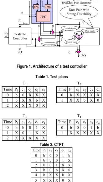
The architecture of a test controller proposed in [5] is summarized. Figure 1 shows the test controller which supplies test plans to control signals of the data path with strong testability. The test controller consists of a test plan generator (TPG), a test pattern register (TPR), and a target module register (TMR) as shown in Figure 1. Consider the test of a combinational module M, which has data inputs and control inputs, in the data path. The TMR is used to store the index of M. The bit width of the TMR is
ª
log2nº
, where n is the number of combinational modules in the data path. The TPG generates the test plan of M from the index stored in the TMR. Thus, the TPG supplies the values in n test plans to control signals. The number of states in the TPG is max(Li), where Liis the length of a test plan for a combinational module i. When the data input value of a test pattern of M is justified, if some primary inputs of the data path are not used, the control input value is applied from such primary inputs by way of the TPG. Otherwise, the control input value is pre-stored in the TPR and is applied to the control inputs by way of the TPG. If the Reset is applied, the TPR and the TMR load values from some primary inputs of the data path, otherwise, they hold their values. The mode switching signal t1 is used to disable DFT elements of the data path in normal operation mode. In [5], the detailed architecture of the TPG was not described. If a data path has many test plans, the TPG is not synthesizable.
In [5], testing is sequentially performed for a single combinational module in data paths. The test length for data paths with strong testability using this test controller is, then, given by
L=¦ + ×
= n i
i
i N
L
1
) ) 1
(( , (1)
where L is the test length for data paths, n is the number of combinational modules, Li is the length of a test plan for a combinational module i (i = 1,2, ..., n), and Ni is the number of test patterns for a combinational module i. Li+1 cycles are required to apply one test pattern to a combinational module because one cycle is required to load values into the TPR and the TMR. Equation (1) shows that the test length for data paths with strong testability becomes drastically longer as the number of combinational modules and the number of gates in
a combinational module increase.
Example 1: Table 1 shows the four test plans T1, T2, T3 and T4
for the combinational modules 1, 2, 3, and 4 in the data path, respectively. P1 shows the primary input of a data path and c1, c2, c3, and c4 show the control signals of a data path. A test plan has four kinds of values 0, 1, X (don’t care), and b. b is the value which constitutes a test pattern to detect a fault in a combinational module [12]. The bit width of the TMR is 2 because the number of test plans is 4, the bit width of the TPR is 1 because the number of b’s of control signals in a test plan is 1, and the number of states in the TPG is 3 because the maximum length of test plans is 3. The numbers of test patterns for the combinational module 1, 2, 3, and 4 are 8, 3, 7, and 2, respectively. The test length for the data path is, according to equation (1), (3+1) × 8+ (2+1) × 3+ (3+1) × 7+ (2+1) × 2 =75.
Figure 1. Architecture of a test controller Table 1. Test plans
Table 2. CTPT
2.2 Supply of a CTPT by a Test Controller
All test plans are compacted using the algorithm proposed Time P1 c1 c2 c3 c4 Time P1 c1 c2 c3 c4
0 b 0 X X X 0 b X X X X
1 b X X b X 1 X X b X 0
2 X X X 0 X
Time P1 c1 c2 c3 c4 Time P1 c1 c2 c3 c4
0 b b 0 1 X 0 b 0 0 1 b
1 X 0 1 X X 1 X X X X X
2 X X X X X
T1 T2
T3 T4
Time P1 c1 c2 c3 c4
0 b 0 0 1 b
1 b b 0 1 X
2 b 0 1 X X
3 b 0 b X 0
4 b X X b X
5 X X X 0 X
Testable Controller
PI
PO
PI
PO
TPR
TPG TPG
TMR
Test Controller
t0
t2 t3
t4
t1 t1
Reset
TPR: Test Pattern Register TMR FTarget Module Register TPG FTest Plan Generator
M Data inputs
Control input Control signals
Status signals
Data Path with Strong Testability
in [12], and a resultant CTPT is generated. Combinational modules are tested using a CTPT.
Example 2: Table 2 shows the CTPT which is generated to minimize the length from 4 test plans shown in Table 1.
Consider a test controller of a CTPT based on the test controller shown in Figure 1. The TMR is unnecessary. The TPG generates the values of control signals in a CTPT. The number of states in the TPG is LCTPT, where LCTPT is the length of a CTPT. While testing combinational modules, if the primary inputs which drive the TPR are not used, the control input values can be reloaded into the TPR using the test controller shown in Figure 2. In Figure 2, if the control input values are reloaded into the TPR, the value of the reload signal is 1, otherwise is 0. If a test controller does not have the reload function, the bit width of the TPR is the number of b’s of control signals in a CTPT. Thus, the reload function is necessary to reduce the bit width of the TPR.
The test length for data paths with strong testability using this test controller is, then, given by
L=max(Ni) × (LCTPT+1), (2)
where L is test length for data paths and Ni is the number of test patterns for a combinational module i.
The area of the TPG is very large when LCTPT is large. Thus, it is considered that the test controller to generate the values of control signals in a CTPT is not practical. It is also predicted that the test length by a test generation using a CTPT is long for data paths with the following characteristics.
1. The maximum number of test patterns for a combinational module and the minimum number of test patterns for the other combinational modules are very different.
2. The number of combinational modules with the maximum number of test patterns is small and the number of combinational modules with the minimum number of test patterns is large.
Example 3: In the CTPT shown in Table 2, the bit width of the TPR is 4. The values of control signals can be loaded into the TPR at time -1. The number of states in the TPG is 6 because the length of the CTPT is 6. The test length for the data path is, according to equation (2), 8 × (6+1) = 56.
3. Test Generation Method Using Several Partly Compacted Test Tables
In this section, a test generation method using several partly compacted test plan tables is proposed to shorten test length compared with the conventional methods described in section 2. The optimization problem for test plan grouping is formulated using ILP.
3.1 Preliminaries
(Definition 1: Partly compacted test plan table)
A subset of a test plan set is compacted and the resultant one is
referred to as a partly compacted test plan [12]. Especially, when a partly compacted test plan is used for test generation, it is referred to as a partly compacted test plan table (PCTPT). Example 4: Table 3 shows the two PCTPTs (PCTPT1 and PCTPT2). Four test plans shown in Table 1 are partitioned into two groups (G1 and G2), PCTPT1 is generated from G1, and PCTPT2 is generated from G2 by applying the algorithm shown in [12].
Figure 2. Test controller with reload function
Table 3. Two PCTPT
Table 4. Drive control signal table
Figure 3. Architecture of TPG (Definition 2: Density degree)
The density degree DDTi for a test plan Ti shows the number of 0’s, 1’s, and b’s in Ti and is given by the following equation.
c1 c2 c3 c4 c1 c2 c3 c4
1 0 1 0 0 1 0 1
c1 c2 c3 c4 c1 c2 c3 c4
1 1 1 0 1 1 1 1
DC3 DC4
DC1 DC2
FSM
t1
Reset
MUX Decoder-G1
Decoder-Gj
Decoder-Gm
TPR TMR
c1
c2
ck
cu
GL1
GL‚Š
GLm
GNC1
GNC‚Š
GNCm
Decoder
PI (Data path)
TPR
TPG TPG
TMR
Test Controller
t1
Reset (Controller)
Control signals (Data path)
Reload signal
Time P1 c1 c2 c3 c4 Time P1 c1 c2 c3 c4
0 b3 b3 0 1 X 0 b4 0 0 1 b4
1 b1 0 1 X X 1 b2 X X X X 2 b1 X X b1 X 2 X X b2 X 0
3 X X X 0 X
PCTPT1 PCTPT2
DDTi = {( 0 1 ) }
1
ki k u
k
k
k c cb
c + + ×δ
¦
=
,
where u is the number of control signals, c0k is the number of 0’s of the control signal ck in Ti, c1k is the number of 1’s of the control signal ck in Ti, cbk is the number of b’s of the control signal ck in Ti, and δkiis the 0-1 variable.
If one of the following conditions is at least satisfied, δkiis 0. Otherwise, δkiis 1.
(C1) c0k and cbk are 0. (C2) c1k and cbk are 0.
(C3) c0k and c1k are 0, and cbk is 1.
Example 5: The density degrees DDT1, DDT2, DDT3, and DDT4
are 2, 0, 4, and 0, respectively.
(Definition 3: Drive control signal table)
The drive control signal table DCi for a combinational module i shows the control signals where a test plan Ti is supplied. The column of a DCirepresents a control signal ck (k = 1,2, ..., u), where u is the number of control signals of a data path. The row of a DCi represents flags to show whether Ti is supplied to control signals or not. The value of a flag for ck in DCi is denoted by DCi(ck). Thus, when there exists 0, 1, or b at any time for a control signal ck in Ti, DCi(ck) is 1. Otherwise, DCi(ck) is 0.
Example 6: Table 4 shows the drive control signal tables DC1, DC2, DC3, and DC4 for the test plans T1, T2, T3, and T4, shown in Table 1, respectively.
3.2 PCTPT Generation and Architecture of TPG A test generation method using several PCTPTs is proposed to shorten test length. A test plan set is partitioned into m groups Gj (j = 1, 2, ..., m, and m is the number of groups). A CTPT for each group is generated. If Ti and Th belong to Gj, Ni
is maximum, and (Ni – Nh ) is small, the test length is drastically improved, where Ti, Th, Ni, and Nh are the test plan for module i, the test plan for module h, the number of test patterns for module i, and the number of module h, respectively.
The architecture of the TPG in a test controller is proposed to synthesize the TPG in a reasonable time. Figure 3 shows the architecture. The TPG consists of the FSM, the Decoder, and MUX. When the number of states in the FSM is large and the number of control signals is large, the area of the Decoder drastically increases. Therefore, it is very difficult to synthesize the TPG. In Figure 3, the Decoder is divided into m decoders for each PCTPT. Let GLj be the length of PCTPTj, Decoder-Gj be a decoder for PCTPTj and GNCj be the number of control signals where the values in PCTPTj are supplied. The MUX is an array of multiplexers. The Decoder consists of mis the decoders Decoder-Gj. The maximum value of the length of the PCTPTj is the number of states in the FSM, and affects the area of the FSM. The density degree of PCTPTj
affects the area of the Dcoder-Gj. ¦
= m
j
GNCj 1
affects the area of the MUX. Thus, the test controller area and test length for data paths can be reduced by considering the test plan grouping.
3.3 Test Plan Grouping Method
In this subsection, the optimization problem for test plan grouping is formulated using ILP as follows.
(1) Input
(a) n test plans Tiand the number of test patterns Ni
(1≤i≤n, n is the number of test plans) (b) The number of groups: m (1≤m≤n) (c) Constraint q
q means max
j
(GNCj). ( max i
(¦
= u k
k ic
DC
1
)
( ) ≤ q≤u, u is the number of control signals in a data path)
GNCjis given by the following equation. GNCj = ¦
= = u
k n i 1 1
‡X(Xij
×
DCi(ck))The following 0-1 variable Xij is defined as an ILP variable. Xij= 1 (Ti belongs in Gj), Xij = 0 (Otherwise)
(d) Constraint p p means max
j
(¦
=
×
n i
i
ij L
X
1
)
( ). ( max
i
(Li)
≤
p≤
¦= n i
Li 1
) (e) Constraint r
All test plans in Gj are concatenated, the resultant one is referred to as a concatenated test plan of Gj, and it is denoted by CTj. All test plans in a data path are concatenated, the resultant one is referred to as a concatenated test plan of a data path, and it is denoted by CTall.
r means max
j
(DDCTj). ( max i
(DDTi) ≤ r
≤
DDCTall) (2) Outputm test plan sets Gj (1
≤
j≤
m)(3) Optimization: minimize the following cost function F
F = ¦ ¦ − × ×
= = m j
n i
ij i i
j N L X
MAXTP
1 1
) )
(( MAXTPj= max
i
(Xij
×
Ni) Constraints(c1) max
j
(GNCj)≤q (c2) max
j
(¦
=
×
n i
i
ij L
X
1
)
( )≤p
(c3) max
j
(DDCTj)
≤
r (c4) ¦= m
j
Xij 1
=1 (c5) ¦
= n
i
Xij 1
≥
1The cost function F is the total sum of the length of unnecessary test sequence for each combinational module and it is expected that the test length is reduced by minimizing F. (c1) means that the maximum output number of Decoder-Gj in the TPG is less than or equal to q. The area of the MUX in the TPG is reduced by adjusting q. (c2) means that the maximum value of the total sum of each test plan length in Gj is less than or equal to p. The area of the FSM in the TPG is reduced by adjusting p. (c3) means that the maximum value of the density
degree of Gj is less than or equal to r. The area of the Decoder in the TPG is reduced by adjusting r. (c4) means that a test plan Ti belongs to only one group. (c5) means that Gj is not empty.
3.4 Test Generation
After a gate level circuit for a combinational module is synthesized, test generation is performed for a single stuck-at-fault in a combinational module. As a result, test patterns for a combinational module are generated. Next, bj’s corresponding to a test pattern for each combinational module j (j = 1, 2, ..., n) are replaced with the test pattern (0’s and/or 1’s). The above-mentioned processing is iterated for all test patterns for each combinational module j. The test length for a data path circuit with strong testability is given by
L = ¦
=
×
m
j j
PCTPT
j L
MAXTP
1
, (3) where MAXTPj= max
i
(Xij× Ni), LPCTPTj is the length of
PCTPTj, Ni is the number of test patterns for a combinational module i, and L is the test length for a data path circuit. Example 7: In the PCTPTs shown in Table 3, the bit width of the TPR is 2. The values of control signals are loaded into the TPR at time –1. The number of states in the FSM is 4 because the length of max
i
(LPCTPTj) is 4. The test length for the data path is, according to equation (3), 8
×
(4+1)+3×
(3+1)=52. 4. Experimental ResultsIn this section, the experimental results of the test generation method using several PCTPTs are described by applying it to some practical RTL data paths.
The platform of the preliminary experiments is as follows. CPU: Pentium , Frequency: 1GHz,
and Memory: 512Mbyte.
The characteristics of the practical RTL data paths with strong testability are shown in Table 5. Circuit, #PI, #PO, #CS,
#ST, #R, #M, and |bit| denote the circuit name, the number of primary inputs, the number of primary outputs, the number of control signals, the number of status signals, the number of registers, the number of combinational modules, and the bit widths of data path signals, respectively. The logic synthesis was performed using the Design Compiler® of Synopsys and the test generation for each combinational module was performed using the TetraMax® ATPG of Synopsys.
The proposed method was compared with three conventional methods: the test generation method using test plans [5], and the test generation method using a CTPT [12]. In the test generation method using a CTPT, the test controller area could not be synthesized for three data paths. Therefore, we concluded that it is difficult to apply the test generation method using a CTPT to practical data paths. Thus, we will not refer to the test generation method using a CTPT from now on.
In Table 6, Circuit denotes circuit name, “PCTPT” shows
the experimental results of the test generation method using several PCTPTs, “PCTPT-TA10” shows the experimental results of the test generation method using several PCTPTs with less than 10 % additional test controller area,
“PCTPT-TA30” shows the experimental results of the test generation method using several PCTPTs with less than 30 % additional test controller area, “TP” shows the experimental results of the test generation method using test plans [5], and
“CTPT” shows the experimental results of the test generation method using a CTPT [12]. In Table 6, m denotes the number of groups, TL denotes the test length for data paths, and TA denotes the area of a test controller. RTL and RTA of “PCTPT” are defined as follows. RTL and RTA of “PCTPT-TA10” (“PCTPT-TA30”) are also defined in the same way as those of
“PCTPT”. p, q, and r are parameters.
RTL = (TL of “TP” – TL of “PCTPT”) / TL of “TP” RTA=(TA of “PCTPT” – TA of “TP”) / TA of “TP”
In “PCTPT”, p, q, and r were set to 2000, infinity, and 3000. Given m, test plans were partitioned into m groups to shorten test length. “PCTPT” shortened the test length by 30 to 54 % compared with “TP”. However, the test controller area increased by 10 to 122 % compared with “TP”. As for test controller area, the area of “TP” was minimum except for IDCT.
In “PCTPT-TA10” (“PCTPT-TA30”), p, q, and r were set to optimum values to shorten test length with less than 10 % (30 %) additional test controller area compared with “TP”. The values of these parameters were determined taking the following (1), (2), and (3) into account.
(1) p affects the area of the FSM in the TPG. (2) q affects the area of the MUX in the TPG. (3) r affects the area of the Decoder in the TPG.
“PCTPT-TA10” shortened the test length by 4 to 36 % with less than 10 % additional test controller area compared with
“TP”. “PCTPT-TA10” could not find the values of the parameters to shorten the test length with less than 10 % additional test controller area for MPEG. “PCTPT-TA30” shortened the test length by 6 to 54 % compared with “TP”. As for MPEG, “PCTPT-TA10” reduced the test controller area by 9 % compared with “TP”.
Table 5. Characteristics of RTL data paths
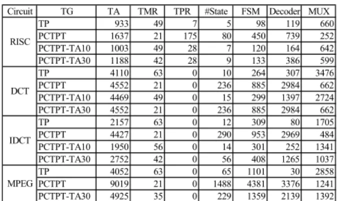
Table 7 shows the detailed area of the test controllers. In Table 7, “TG” denotes a test generation method, “TA” denotes the test controller area, “TMR” denotes the area of the TMR,
“TPR” denotes the area of the TPR, “#State” denotes the number of states in the FSM, “FSM” denotes the area of the FSM in the TPG, “Decoder” denotes the area of the Decoder in the TPG, and “MUX” denotes the area of the MUX in the TPG. As for “PCTPT”, “TMR”, and “MUX” were reduced, and
Circuit #PI #PO #CS #ST #R #M |bit|
RISC 32 96 177 5 47 115 32
DCT 96 224 112 2 22 312 32
IDCT 96 224 135 6 27 349 32
MPEG 56 128 589 0 241 368 8
“TPR”, “FSM”, and “Decoder” were increased compared with
“TP”. As for “PCTPT-TA10” and “PCTPT-TA30”, by setting the value of p to the optimum value, the maximum value of the lengths of PCTPTs was shortened, and “FSM” was reduced compared with “PCTPT”. By setting the value of r to the optimum value, the maximum value of the density degree of PCTPTs was reduced, and “Decoder” was reduced compared with “PCTPT”. By setting the value of q to the optimum value, the maximum number of control signals where the values in PCTPTs were supplied was reduced,
“MUX” was reduced compared with “TP”, and “MUX” was increased compared with “PCTPT”.
5. Conclusion
This paper proposed a test generation method using several PCTPTs for RTL data path. The optimization problem for test plan grouping is also formulated using ILP to shorten test length under a test controller area constraint. Experimental results for practical RTL data paths show that the test lengths are shortened by 4 to 36% with less than 10 % additional test controller area and the test lengths are shortened by 6 to 54% with less than 30 % additional test controller area compared with the test generation method using test plans. Future work includes proposing an effective algorithm for finding the optimum values of the parameters.
Acknowledgements
This work was sponsored by NEDO (New Energy and Industrial Technology Development Organization) as VCDS Project (SoC advanced design technology development project). The Authors would like to thank Prof. Michiko Inoue, Prof. Satoshi Ohtake, and Prof. Tomokazu Yoneda of Nara Institute of Science and Technology for their valuable discussion and comments. The Authors would like to thank Prof. Tomoo Inoue and Prof. Hideyuki Ichihara of Hiroshima City University for his valuable discussion and comments. The Authors would like to thank Dr. Rafael K. Morizawa of STARC for his valuable comments.
References
[1] H. Fujiwara, “Logic Testing and Design for Testability,” The MIT Press, 1985
[2] M. Abramovici, M. A. Breuer, and A. D. Friedman, “Digital systems testing and testable design,” IEEE Press, 1995.
[3] T. Hosokawa, M. Yoshimura, and M. Ohta, “Design for testability strategies using full/partial scan designs and test point insertions to reduce test application times,” Proc. of Asia and South Pacific Design Automation Conference, pp.485-491, 2001.
[4] P. C. Maxwell, R. C. Aitken, V. Johansen, and Chiang, “The effect of different test sets on quality level prediction:
When is 80% better than 90 %?,” in Proc. of International Test Conference, pp.358-364, 1991.
[5] S. Ohtake, H. Wada, T. Masuzawa, and H. Fujiwara, “A Non-Scan DFT Method at Register-Transfer Level to Achieve Complete Fault Efficiency,” Proc. of Asia and South Pacific Design Automation Conference, pp.599-604, 2000.
[6] S. Ohtake, S. Nagai, H. Wada, and H. Fujiwara, “A DFT Method for RTL Circuits to Achieve Complete Fault Efficiency Based on Fixed-control Testability,” Proc. of Asia and South Pacific Design Automation Conference, pp.331-334, 2001.
[7] I. Ghosh, A. Raghunathan and N.K. Jha, “Design for hierarchical Testability of RTL circuits obtained by behavioral synthesis,” IEEE Trans. on Computer Aided Design, Vol.16, No.9, pp.1001-1014, 1997.
[8] I. Ghosh, A. Raghunathan and N.K. Jha, “Hierarchical test generation and design for testability methods for ASPP’s and ASIP’s”, IEEE Trans. on Computer Aided Design, Vol.18, No.3, pp.357-370, 1999.
[9] H. Wada, T. Masuzawa, K.K. Saluja, and H. Fujiwara, “Design for strong testability of RTL data paths to provide complete fault efficiency,” Proc. of 13th Int. Conf. on VLSI Design, pp.300-305, 2000.
[10] S. Nagai, S. Ohtake, and H. Fujiwara, “A design for hierarchical testability for RTL data paths using extended data flow graphs,” Proc. of Workshop on RTL ATPG & DFT (WRTLT), pp.128-133, 2001. [11] B.T. Murray and J.P. Hayes, “Hierarchical test generation using pre computed tests for modules,” IEEE Trans. on Computer Aided Design, Vol.9, No6, pp.594-603, 1990.
[12] T. Hosokawa, H. Date, and M. Muraoka, “A Test Generation Method Using a Compacted Test Table and a Test Generation Method Using a Compacted Test Plan Table for RTL Data Path Circuits,” Proc. of 20th IEEE VLSI Test Symposium (VTS2002), pp.328-335, 2002.
Table 7. Characteristics of test controllers
Table 6. Experimental results
Circuit TG TA TMR TPR #State FSM Decoder MUX
TP 933 49 7 5 98 119 660
PCTPT 1637 21 175 80 450 739 252
PCTPT-TA10 1003 49 28 7 120 164 642
PCTPT-TA30 1188 42 28 9 133 386 599
TP 4110 63 0 10 264 307 3476
PCTPT 4552 21 0 236 885 2984 662
PCTPT-TA10 4469 49 0 15 299 1397 2724
PCTPT-TA30 4552 21 0 236 885 2984 662
TP 2157 63 0 12 309 80 1705
PCTPT 4427 21 0 290 953 2969 484
PCTPT-TA10 1950 56 0 14 301 252 1341
PCTPT-TA30 2752 42 0 56 408 1265 1037
TP 4052 63 0 65 1101 30 2858
PCTPT 9019 21 0 1488 4381 3376 1241
PCTPT-TA30 4925 35 0 229 1359 2139 1392
IDCT
MPEG RISC
DCT
m TL TA RTL(%) RTA(%) m TL TA RTL(%) RTA(%) p q r m TL TA RTL(%) RTA(%) p q r TL TA TL TA RISC 8 3216 1637 37.8 75.5 97 4924 1003 4.8 7.5 8 32 14 54 4219 1188 18.4 27.3 10 38 16 5172 933 41940 1535 DCT 7 10392 4552 54.8 10.8 124 14487 4469 36.3 8.7 24 195 36 7 10392 4552 54.8 10.8 22744 4110 23630 NA IDCT 8 15316 4427 44.9 105.3 160 17818 1950 36.0 -9.6 24 205 36 40 15901 2752 42.8 27.6 96 287 144 27819 2157 64912 NA
MPEG 7 77011 9019 30.9 122.3 32 104457 4925 6.3 21.5 384 412 576 111495 4052 96269 NA
Circuit PCTPT PCTPT-TA10 PCTPC-TA30 TP CTPT