1022 IEEE TRANSACTIONS ON COMPUTER-AIDED DESIGN. VOL 8. NO
zyxwvutsrqponmlkjihgfedcbaZYXWVUTSRQPONMLKJIHGFEDCBA
9. SEPTEMBERzyxwvutsrqponmlkjihgfedcbaZYXWVUTSRQPONMLKJIHGFEDCBA
19x9Short
Enhancing Random-Pattern CoveragePapers zyxwvutsrqponmlkjihgfedcbaZYXWVUTSRQPONMLKJIHGFEDCBA of
Programmable Logic Arrays via Masking Technique
HIDE0 FUJIWARA, FELLOW,
zyxwvutsrqponmlkjihgfedcbaZYXWVUTSRQPONMLKJIHGFEDCBA
I t t EAbstract-This paper presents a testable design of programmable logic arrays (PLA’s) with high fault coverage for random test patterns. The proposed design is realized with low area overhead by adding two
mask arrays to the A N D and
zyxwvutsrqponmlkjihgfedcbaZYXWVUTSRQPONMLKJIHGFEDCBA
OR arrays of the PLA. To demonstrate theeffect of the masking technique, an experiment was performed in which eight large PLA’s were modified by adding various sizes of mask ar- rays, and then fault simulation with random patterns for those modi- fied and unmodified PLA’s was carried out to obtain random-pattern test coverage curves. It was found that fault coverage can be signifi- cantly enhanced via the proposed masking technique with very low area overhead.
I. INTRODUCTION
Programmable logic arrays (PLA’s) are very suitable to VLSI and have become a popular and effective tool for implementing logic functions because of their regular structure. On the other hand, the built-in self-test (BIST) approach using linear feedback shift registers (LFSR’s) is currently being widely investigated as an at- tractive testing technique for VLSI circuits [ l ] . The major difficulty in random testing using LFSR-generated pseudorandom patterns is the low fault coverage for very high fan-in circuits such as PLA’s. Hence, for BIST PLA’s it is necessary either to employ determin- istic (not random) test patterns or to augment a PLA to make it random-pattern-testable. The former includes BIST PLA designs with universal test patterns [2]-[6]. Although these BIST PLA’s can achieve very high fault coverage, the area overhead is still high. For the latter approach, two random-pattern-testable designs of PLA’s were proposed by Eichelberger and Lindbloom [7] and Ha
and Reddy
zyxwvutsrqponmlkjihgfedcbaZYXWVUTSRQPONMLKJIHGFEDCBA
[ 5 ] . However, these methods also have high area over-head due to their extra circuitry for controlling a large number of product lines of PLA’s.
In [9], we proposed an approach to designing a random-pattern- testable PLA with very low area overhead by adding a mask array only between the input decoder and the A N D array. We estimated the number of random patterns necessary for achieving a given test confidence by analyzing the detection probability of stuck-at and crosspoint faults. In this paper, we shall propose an improved de- sign based on the approach of [9] in which a mask array is added to the OK array in addition to the A N D array of a PLA. T o demon- strate the effect of the masking technique, an experiment was per- formed in which eight large PLA’s were modified by adding var- ious sizes of mask arrays, and then fault simulation with LFSR- generated pseudorandom patterns for those modified and unmodi- fied PLA’s was carried out to obtain fault coverage curves. We shall present the experimental results: real fault coverage curves for the eight large PLA’s to demonstrate the effect of masking tech- nique. It has been found that fault coverage can be significantly
Manuscript received April 4, 1988; revised November
zyxwvutsrqponmlkjihgfedcbaZYXWVUTSRQPONMLKJIHGFEDCBA
3 , 1988. TheThe author is with the Department of Computer Science, Meiji Univer- lEEE Log Number 8928247.
review of this paper was arranged by Associate Editor V . K. Agarwal.
sity. Kawasaki 214, Japan.
enhanced via the masking technique proposed in this paper while keeping the area overhead very low.
11. RANDOM-PATTERN-TESTABLE PLA’s
A PLA consists of three main sections: a decoder, an A N D array, and an OR array. The decoder section usually consists of a collec- tion of one-input o r two-input decoders. Both the A N D array and the OR array are used to implement multi-output combinational logic with sum-of-product forms. A PLA is tvpically implemented as a
NOR-NOR array in nMOS technology.
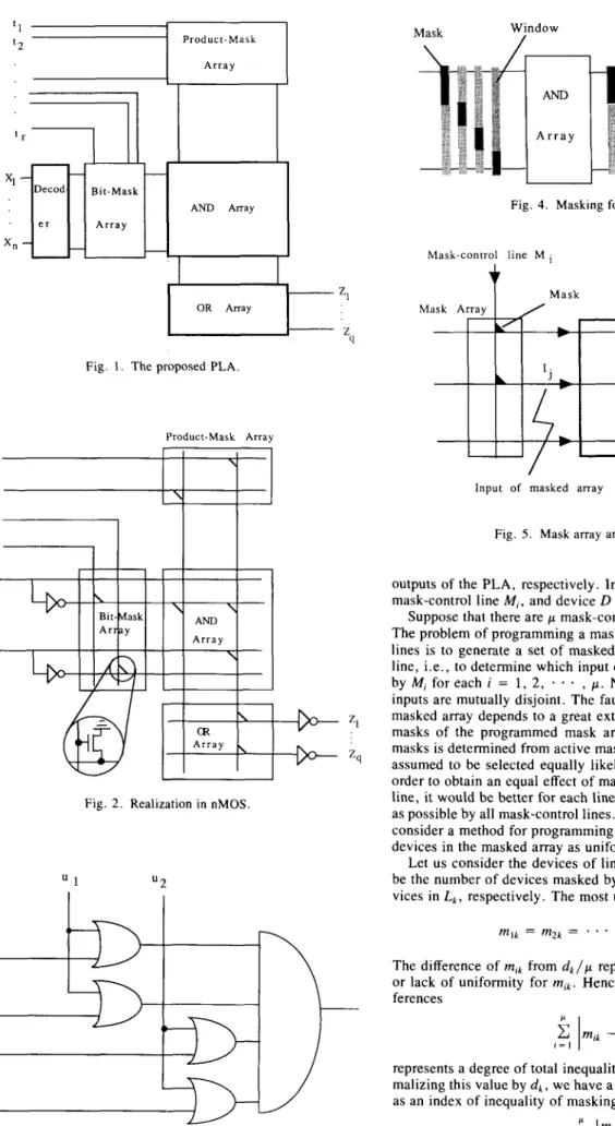
Fig. 1 shows the design of random-pattern-testable PLA’s pro- posed in this paper. The augmented PLA has additional circuitry
consisting of two programmable mask arrays, called the
zyxwvutsrqponmlkjihgfedcbaZYXWVUTSRQPONMLKJIHGFEDCBA
bit-maskarray and the producr-mask array, which selectively mask the in- puts of the A N D array and the OR array, respectively. These mask arrays are programmed to increase the fault coverage of the PLA effectively, and are activated by extra inputs I , , f 2 ,
. . .
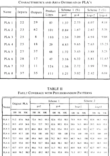
, t , . These control inputs are all set to value zero during functional operation. Fig. 2 shows an example of the proposed PLA with mask decoders in nMOS technology.The principle of masking is illustrated in Fig. 3 using an A N D -
OR equivalent circuit. In the figure, by controlling
zyxwvutsrqponmlkjihgfedcbaZYXWVUTSRQPONMLKJIHGFEDCBA
U , = 0, u2 = I ,a3 and a, are masked and only the inputs of a , and a: are applied to the A N D gate. This causes the fan-in of the A N D gate to decrease from 4 to 2. Here, the control lines U , and u2 are called mask-
control lines, the masked inputs a3 and a, are called mask, and unmasked inputs such as a , and a2 are called window. W e consider the masking form which is illustrated in Fig. 4. The form is mask- disjoint; i.e., no pair of masks overlap each other and the union of all masks covers the fan-in of all A N D and O R arrays.
We shall consider two schemes of PLA’s which are random- pattern-testable as follows:
Scheme 1: The augmented PLA with the bit-mask array but without the product-mask array.
Scheme 2 : The augmented PLA with both the bit-mask and product-mask arrays.
We assume that random patterns are applied not only to the pri- mary inputs of the PLA but also to the mask-control inputs in test- ing. Hence, in the augmented PLA, more than two mask-control lines may be active. Mask-disjoint form of masking is thus useful to this scheme. As illustrated in Fig. 3, the purpose of masking is to decrease the fan-in of A N D and OR arrays in order to increase the fault detection probability. Those mask arrays should be pro- grammed to enhance most effectively the fault coverage of the PLA. In the next section, we shall present a method of programming mask patterns for mask arrays.
111. PROGRAMMING MASK PATTERNS
The most effective mask arrays that yield the maximum enhance- ment of fault detection probability could be obtained by consider- ing the detailed connection information of both the A N D and OR
arrays. However, it is a difficult and time-consuming problem to obtain the optimum solution. Here we shall consider a simple method of generating mask patterns for each of the A N D and O R
arrays separately.
Let us consider a mask array and a masked array shown in Fig. 5. When the masked array is an A N D array, inputs and outputs of the masked array correspond to bit lines and product lines of the PLA, respectively. When the masked array is an OK array, inputs and outputs of the masked array correspond to product lines and
0278-0070/89/0900-1022$01 .OO
zyxwvutsrqponmlkjihgfedcbaZYXWVUTSRQPONMLKJIHGFEDCBA
0 1989 IEEEIEEE
zyxwvutsrqponmlkjihgfedcbaZYXWVUTSRQPONMLKJIHGFEDCBA
TRANSACTIONS ON COMPUTER-AIDED DESIGN, VOL. 8. NO. 9. SEPTEMBER 1989 1023Array
zyxwvutsrqponmlkjihgfedcbaZYXWVUTSRQPONMLKJIHGFEDCBA
I
zyxwvutsrqponmlkjihgfedcbaZYXWVUTSRQPONMLKJIHGFEDCBA I I
OR Array
4
Fig. 1. The proposed PLA.
Product-Mask Array
‘ 1
‘ 2
‘ 3
‘ 4
zyxwvutsrqponmlkjihgfedcbaZYXWVUTSRQPONMLKJIHGFEDCBA
X1
Xn
Fig. 2 . Realization in nMOS.
“ 1
Window
Mask /
\
/.
A r r a y AND
A r r a y
Fig. 4. Masking form of PLA.
Mask-control line M
L k
I
Masked ArravM a s k
Mask Array /
/
Input of masked array
Output of masked array
Fig.
zyxwvutsrqponmlkjihgfedcbaZYXWVUTSRQPONMLKJIHGFEDCBA
5 . Mask array and masked arrayoutputs of the PLA, respectively. In Fig. 5, input I, is
zyxwvutsrqponmlkjihgfedcbaZYXWVUTSRQPONMLKJIHGFEDCBA
masked bymask-control line M , , and device
zyxwvutsrqponmlkjihgfedcbaZYXWVUTSRQPONMLKJIHGFEDCBA
D is also masked by M , .Suppose that there are p mask-control lines, M , , M z ,
. . .
, M,.The problem of programming a mask array for those mask-control lines is to generate a set of masked inputs for each mask-control line, i.e., to determine which input of the masked array is masked by M , for each i = 1, 2,
. .
* , p . Note that these sets of masked inputs are mutually disjoint. The fault detection probability of the masked array depends to a great extent on the size of windows or masks of the programmed mask array. The size of windows or masks is determined from active mask-control lines, which will be assumed to be selected equally likely by random test patterns. In order to obtain an equal effect of masking from each mask-controlline, it would be better for each line Lk
zyxwvutsrqponmlkjihgfedcbaZYXWVUTSRQPONMLKJIHGFEDCBA
to be masked as uniformlyas possible by all mask-control lines. From this viewpoint, we shall consider a method for programming a mask array which masks all devices in the masked array as uniformly as possible.
Let us consider the devices of line L, in Fig. 5. Let mtk and dk be the number of devices masked by M, and the number of all de- vices in Lk, respectively. The most uniform masking occurs when
The difference of mrk from d k / p represents a degree of inequality or lack of uniformity for mik. Hence the summation of those dif- ferences
represents a degree of total inequality of masking for line Lk. Nor- malizing this value by d k r we have a measure Dk which can be used as an index of inequality of masking with respect to line L,: Fig. 3 . Masking of A N D gate
1024 IEEE TRANSACTIONS ON COMPUTER-AIDED DESIGN, VOL. 8. NO. 9. SEPTEMBER
zyxwvutsrqponmlkjihgfedcbaZYXWVUTSRQPONMLKJIHGFEDCBA
I Y X YzyxwvutsrqponmlkjihgfedcbaZYXWVUTSRQPONMLKJIHGFEDCBA
Vame
, L A 1
P L A 2
zyxwvutsrqponmlkjihgfedcbaZYXWVUTSRQPONMLKJIHGFEDCBA
P I A 3 P I A 4 P L A ~ I L A 6 P L A ~
P L A 8
zyxwvutsrqponmlkjihgfedcbaZYXWVUTSRQPONMLKJIHGFEDCBA
Procedure f o r Musk Pattern Generation
Scheme 1 Sci,eme
zyxwvutsrqponmlkjihgfedcbaZYXWVUTSRQPONMLKJIHGFEDCBA
2Original PLA
p 2 p 4 h = l d
5M
zyxwvutsrqponmlkjihgfedcbaZYXWVUTSRQPONMLKJIHGFEDCBA
5K 50K 5W 5K 50K SW SK 50K s(XI SK (OK 5lH) > k ,IIK5 1 2 8 7 6 9 6 8 7 2 4 9 4 3 9 9 1 8 2 6 9 2 0 9 8 1 7 1 9 ‘159 9 9 1 X j X
zyxwvutsrqponmlkjihgfedcbaZYXWVUTSRQPONMLKJIHGFEDCBA
‘ 1 x 2 W‘I3 9 3 4 3 9 5 4 6 5 2 4 7 2 7 7 9 2 6 5 6 R03 8 5 4 5 4 6 7 4 ; X X Y 5‘17 X J X
zyxwvutsrqponmlkjihgfedcbaZYXWVUTSRQPONMLKJIHGFEDCBA
9 > 14 8 8 RI10 8 7 2 6 0 4 8 8 4 99.7 5 9 2 9 2 4 9 9 5 ??‘I U 8 5 9 Y : 6 2 7 K l > 100 6 9 9 R73 IW 9 5 8 IM 1W 9 2 7 IN! I W 7 7 6 llYl liII 9 7 7 IOII / ( / / I 7 2 7 9 5 6 I W 69.4 9 6 9 ion 7 9 2 9 x 7 9 9 9 M ? ‘265 I ~ U I 4 2 4 ‘IYY I W
6 3 9 9 3 6 9 9 7 7 9 8 9 3 7 9 8 6 8 6 8 9 6 1 9 8 2 US3 96’2
zyxwvutsrqponmlkjihgfedcbaZYXWVUTSRQPONMLKJIHGFEDCBA
9 8 6 9117 4 x 5 ‘100407 6 7 9 8 7 4 4 6 6 7 1 5 8 4 9 5 1 7 7 0 2 8 3 2 4 9 9 7 x x 9 2 2 6 2 7 X Y ~ ~ W I 6 6 8 9 6 2 98.5 6 9 1 8 9 2 98.7 7 4 6 9SR ! B O 7 1 3 911 9 9 2 X I 4 V U 4 l l l l ’
Step 1 : Calculate current degrees of inequality, D,, for all lines L , ( j = 1,2;.. , A ) .
Step 2 : Find the maximum of D, ( , j = I , 2 ,
. .
. , A). Let L , be a line whose degree of inequality is maximum, i . e . , D , = niax { D, } .Step 3: For the line L,, find the minimum of m,,(i = 1, 2 ,
. . .
, 1). Let Mg be the mask-control line such that m3,= min { mrn } .
Step 4: Add a new mask point to the mask array with respect to mask-control line M O so that mg masks one of the un- masked inputs of line L, to increment m g n . If there are more than two unmasked inputs, then select one whose fan-out is maximum, where the fan-out of an input is the number of lines to which the input fans out. Step 5 : If there remain unmasked inputs, then g o to step 1 . Oth-
erwise, stop.
This procedure does not guarantee that the optimum solution, i.e., the most uniform mask array will be obtained, but it will pro- duce a relatively uniform mask array using a measure of inequa’lity of masking. Uniformity of masking is not our final objective; it is only a shortcut to obtain a mask array which will be expected to enhance the fault detection probability. Further, the correlation be- tween the heuristic used in the above procedure and the actual mask effectiveness is difficult t o show explicitly. Therefore, we would like to study actual PLA’s so see how much the fault coverage would be enhanced after augmentation. In the next section, we shall show the experimental results.
IV. EXPERIMENTAL RESULTS
T o demonstrate the effect of the masking technique, an experi- ment was performed using eight large actual PLA’s, most of which are control logic circuits. These PLA’s were modified to PLA’s embodying two types of schemes by adding various sizes of mask arrays. Then, fault simulation with LFSR-generated pseudorandom patterns for the modified and unmodified PLA’s was carried out to obtain fault coverage curves. In [9], it was shown that the detection probability of crosspoint faults can be represented in the same way as that of stuck-at faults, and so we have considered here only sin- gle stuck-at faults in A N D and OR arrays. In the following, we shall present the experimental results: area overhead for augmented PLA’s and fault coverage enhancement of masking.
A . A r e a O v e r h e a d
Let us estimate the area overhead of two schemes of augmented
PLA’s. Let n , p , and
zyxwvutsrqponmlkjihgfedcbaZYXWVUTSRQPONMLKJIHGFEDCBA
m be the numbers of inputs, product lines,and outputs of the original P L A , respectively. Let and A be the numbers of mask-control lines of bit-mask array and product-mask array, respectively.
W e shall estimate the area by the number o f transistor equiva- lents. Each area of the augmented PLA’s of schemes 1 and 2 can be expressed as follows:
2 n p : m p : 2 p n : Ap: c n :
area of the A N D array, area of the OR array, area of the bit-mask array, area of the product-mask array,
area of the input-decoder of the original PLA, where c is constant.
The area overhead of an augmented PLA is defined as follows: extra area
original area of the PLA
area overhead = x 100%.
Nnme
PLA 1 PLA 2 PLA 3 PLA 4 PLA 5 PLA 6 PLA 7 PLA 8
TABLE 1
CHARACTERISTICS A N D A R E A O V E R H I . A D 01. PLA’s _ _
~
I n p u t s
2 2 2 3 2 5 2 5 2 7 2 8 3 2 3 7
~ _ _ 3 u t p u t s
2 9 6 2 8 1 x 3 7 1 7 1 1 3 5
4 . 8 3 9 6 5 1 . 7 2 3 . 4 3 3 . 1 6 6 . 3 2 1 2 4 1 . 3 6 2 . 7 2 I 1 I 1 . 2 1 3 . 0 2
7 6 3 1 5 7 5 .3 x x 5 ’i 5 . 8 1 I I 6: 3 9 9 7 9 x 2 4 2 6 Ill
TABLE 11
Hence, the area overhead of the PLA of scheme 1 is calculated by area overhead of scheme 1 = 2pn x 100%
2np
+
mp+
cn and that of Scheme 2 is calculated byarea overhead of scheme 2 = 2 p n + x 100%
2np -t mp -t cn
Table I shows the characteristics of eight large PLA’s and the area overheads of the augmented PLA’s of schemes 1 and 2 , where c = 4 is assumed. The fifth through eighth columns show the area overhead of schemes 1 and 2 .
B. Fault C o v e r a g e Enhancement
In Table I1 we have presented the results on fault coverage with 500, 5000, and 50 000 pseudorandom patterms for each PLA. Among the eight PLA’s, three original PLA’s, # 2 , # 3 , and # 7 , are pseudorandom-pattem resistant; i.e., fault coverages for those PLA’s are low after fault simulation even with 50 000 pseudoran- dom patterns, a s shown in Table 11. After modification, scheme 1 achieved high fault coverage for PLA #3 but not for PLA’s #2 and
#7. On the contrary, scheme 2 was able to achieve very high fault coverage for all PLA’s, especially in the case where p = A = 4.
Fig. 6 shows fault-coverage curves with unmodified and four modified schemes for PLA # 2 . The unmodified PLA had a 43.9 percent fault coverage with 5000 patterns and a 54.6 percent cov- erage with 50 000 patterns. T h e modified PLA of scheme 1 could not reach a 90 percent fault coverage after 50 000 patterns. The
IEEE TRANSACTIONS ON COMPUTER-AIDED DESIGN. VOL.
zyxwvutsrqponmlkjihgfedcbaZYXWVUTSRQPONMLKJIHGFEDCBA
X. NO 9. S E P I E M B E R 1989 1025zyxwvutsrqponmlkjihgfedcbaZYXWVUTSRQPONMLKJIHGFEDCBA
t d l l l , Coverage (%)
. ,, ,,
Schcme
zyxwvutsrqponmlkjihgfedcbaZYXWVUTSRQPONMLKJIHGFEDCBA
2 W k 4 190
-
Scheme I (p=4)Scheme
zyxwvutsrqponmlkjihgfedcbaZYXWVUTSRQPONMLKJIHGFEDCBA
2 (p=h=2)Orlglnal PLA
modified PLA of scheme 2 achieved a 95.4 percent fault coverage
with 50 000 patterns when
zyxwvutsrqponmlkjihgfedcbaZYXWVUTSRQPONMLKJIHGFEDCBA
p = X = 4 . Therefore scheme 2 with p= X = 4 is the best among them for achieving a high fault cover- age.
V. CONCLUSION
W e have proposed a design of random-pattern testable PLA’s. The proposed design is realized with very low area overhead: 0 . 8 4 percent through 15.25 percent for eight benchmark PLA’s. W e have also presented experimental results to show that the fault coverage can be significantly enhanced; for example, a 5 4 . 6 percent fault coverage with 50 000 pseudorandom patterns of an original PLA can be enhanced to 95.4 percent after modification of the PLA with 5.35 percent additional logic. The experimental results show that the proposed approach achieved almost 100 percent fault coverage in pseudorandom testing with very low area overhead for all eight benchmark PLA’s.
ACKNOWLEDGMENT
The author would like to thank Prof. T . Sasao of Kyushu Insti- tute of Technology and T . Yoshimura of the NEC Corporation for their kind offer of benchmark PLA’s. Thanks are also due t o 0. Fujisawa and K . Hikone for their assistance in obtaining the ex- perimental results of this work.
REFERENCES
[ I ] H. Fujiwara, Logic Testing
zyxwvutsrqponmlkjihgfedcbaZYXWVUTSRQPONMLKJIHGFEDCBA
and Design f o r Tesiubility. Cambridge,MA: The MIT Press, 1985.
121 K . A . Hua, J:Y. Jou, and J . A . Abraham, “Built-in tests for VLSI finite-state machines,” in Proc. 14th Int. Svmp. Fault-Tolerunt Com- p u t i n x , 1984, pp. . . 292-297.
R. Treuer, H. Fujiwara, and V . K . Aganvai, “lmplementing a built-
in self-test PLA design,” IEEE Design und Test
zyxwvutsrqponmlkjihgfedcbaZYXWVUTSRQPONMLKJIHGFEDCBA
of Computers, vol. 2,no. 2. pp. 37-48, Apr. 1986.
C-Y. Liu, K . K . Saluja, and J . S . Upadhyaya, “BIST-PLA: A built- i n self-test design of large p ~ 0 g r Z ” a b k logic arrays.” in /‘roc. 24th Design Autornut. Conf. 1987, pp. 385-391.
D.
zyxwvutsrqponmlkjihgfedcbaZYXWVUTSRQPONMLKJIHGFEDCBA
S. Ha and S . M . Reddy. “On BIST PLA’s,” i n Proc. 1987 Int. Test Conf., 1987, pp. 342-351.D. L. Liu and E. J . McCluskey, “Design of large embedded CMOS PLA’s for built-in self-test,” in Proc. 1987IEEE Int. Con$ Computer Design, 1987, pp. 678-681.
E. M. Eichelberger and E. Lindbloom, “Random pattern coverage and
diagnosis for LSSD logic self-test.” IBM J . Res. Develop.,
zyxwvutsrqponmlkjihgfedcbaZYXWVUTSRQPONMLKJIHGFEDCBA
vol. 27,pp. 265-272, May 1983.
D. S . Ha and S . M. Reddy, “On the design of random pattern testable PLA‘s.” in Proc. 1986 Inr. Tesr Conf,, 1986, pp. 688-695.
191 H . Fujiwara, “ A design of programmable logic arrays with random- pattern-testability.” IEEE Truns. Computer-Aided D e ~ i g n . vol. 7. pp. 5-10, Jan. 1988.
Schwarz-Christoffel Transformation for the Simulation
of
Two-DimensionalCapacitance C. K . KOC A N D P. F . ORDUNG
Abstract-An inherent problem in the use of simulators for the de- termination of capacitance in VLSI circuits i s the verification of the reliability of the simulation. The problem i s due to the numerical ap- proximations made in order to achieve a versatile simulation. The Schwarz-Christoffel transformation provides theoretically exact sim- ulation of a limited class of problems consisting of two odd shaped con- ductors embedded in a uniform dielectric. We propose that the Schwarz-Christoffel technique can be used to calibrate simulators de- signed for more general problems.
I. INTRODUCTION
Estimating parasitic capacitance of VLSI buses is a crucial step in computing circuit delay, particularly as packing density in- creases and conductor spacings decrease [ 5 ] . A great deal of effort has been spent in designing simulators which take the cross section geometry of the conductor-dielectric system a s input, and compute the capacitance per unit length between the metal lines [ 2 ] , [3].
The numerical methods to estimate the capacitance are usually CPU intensive, and thus prohibitive for VLSI layouts. Another so- lution is to find geometry-dependent approximate formulas which require short run times and a modest amount of memory [ I ] . An inherent problem in using simulators to estimate the parasitic ca- pacitance is the difficulty of determining the reliability of the pre- dicted capacitance values. The reason for this is that all methods in one way o r another involve approximations which are difficult to evaluate.
The Schwarz-Christoffel conformal mapping technique, on the other hand, does not require a priori approximations. As long as the computations can be performed free of round-off error, the computed value would be the exact capacitance of the conductor- dielectric system. The Schwarz-Christoffel mapping technique provides theoretically exact estimates for a limited class of prob- lems, which can be used to check the reliability of simulators de- signed for more general problems.
11. SCHWARZ-CHRISTOFFEL T R A N S F O R M A T I O N
In this section, we show the application of the Schwarz-Chris- toffel conformal mapping technique for a class of capacitance prob- lems. W e consider a pair of conductors which exhibit symmetry Manuscript received April 29, 1988: revised December 14. 1988, and February 20. 1989. This work was supported by the University of Califor- nia and Rockwell International under the MICRO Grant UC-86-033iC7CJ- 242025. The review of this paper was arranged by Associate Editor D. Rose.
C. K. Koq is with the Department of Electrical Engineering. University of Houston, Houston, TX 77204.
P. F. Ordung is with the Department of Electrical and Computer Engi- neering, University of California. Santa Barbara. CA 93106.
IEEE Log Number 8928243.
0278-0070/89/0900-1025$01 .OO