Test Scheduling for Memory Cores with Built-In Self-Repair
Tomokazu Yoneda†, Yuusuke Fukuda†
∗and Hideo Fujiwara†
†Graduate School of Information Science, Nara Institute of Science and Technology
Kansai Science City, 630-0192, Japan
{yoneda, fujiwara}@is.naist.jp
Abstract
This paper presents a stage-based test scheduling for memory cores with BISR scheme under power constraint. We introduce a model to compute the expected test time for a given test schedule for memory cores with BISR scheme based on pass probabilities, and propose a test scheduling algorithm to minimize the expected test time. Experimen- tal results show a significant expected test time reduction compared to the core-based test scheduling method which minimizes the test time.
keywords: SoC, test scheduling, memory core, built-in self- repair, power consumption.
1 Introduction
Rapid improvements in semiconductor technologies en- able us to create the complex chips called SoCs. The test cost of these monster chips is highly related to the test ap- plication time. In the SoC test environment, cores are tested in a modular fashion [1]. A modular test requires an on- chip test infrastructure in the form of a wrapper per core standardized as IEEE Std. 1500 [2] and test access mech- anisms (TAM). A number of approaches have been pro- posed for wrapper and TAM design including test schedul- ing problem such that the test application time is minimized [3, 4, 5, 6, 7, 8].
Furthermore, with the increasing demand for SoCs to include rich functionality, SoCs are being designed with hundreds of memories with different sizes and frequencies. Memory cores usually occupy a significant portion of the chip area and dominate the manufacturing yield of the chip. Keeping the memory cores at a reasonable yield level is im- portant problem for SoCs. The promising way to solve this problem is to employ built-in self-repair (BISR) scheme for memory cores [9, 10, 11, 12, 13]. Several approaches have been proposed for test scheduling problem for memory cores [14, 15, 16]. However, the test scheduling problem for the memory cores with BISR scheme is not addressed so far. In general, the testing of memory core with BISR scheme consists of the following three stages: (1) test (with BIST circuitry), (2) diagnosis/repair (with built-in repair an- alyzer) and (3) re-test (with BIST circuitry). One impor- tant thing in test scheduling for memory cores with BISR scheme is that all stages are not always executed. For ex- ample, if no fault is detected in first test in stage 1, then, it
∗He is currently with Renesas Technology Corp.
is not necessary to execute the following two stages. An- other important thing is to consider the power consumption during test.
To the best of our knowledge, this paper gives a first dis- cussion and a formulation of the test scheduling problem for memory cores with BISR scheme in production test. Since we cannot predict which stage is necessary to execute or not before test application, we have to consider the worst case where all stages are executed and generate a test schedule for it. Even though we have to consider the worst case, there are some cases where the testing can be terminated before its completion. We extend the abort-on-fail approach used in [17, 18] to the abort-on pass/fail approach for the test scheduling problem in this paper. Furthermore, we intro- duce a model to compute the expected test time for a given test schedule for memory cores with BISR scheme based on pass probabilities, and propose an efficient and effective stage-based test scheduling method by considering that it is not necessary to execute the three stages of each core con- secutively as long as they are executed in keep the order. Experimental results for the modified ITC’02 benchmarks show the effectiveness of the proposed method compared to a core-based test scheduling method which minimizes the test time.
The rest of this paper is organized as follows. Section 2 describes the memory core with BISR function we target in this paper. We introduce an abort-on-pass/fail approach in Section 3 and expected test time calculation in Section 4. We present a test scheduling algorithm in Section 5. Exper- imental results are discussed in Section 6. Finally, Section 7 concludes this paper.
2 Built-In Self-Repairable Memory Core
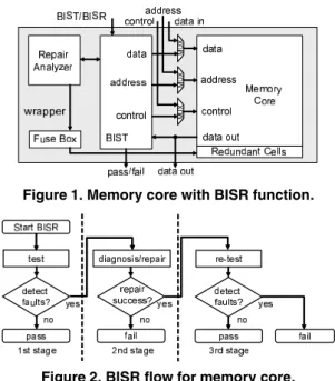
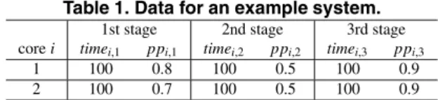
The memory core with BISR function and its test flow we target in this paper are shown in Figure 1 and Figure 2, respectively. It consists of redundant cells, BIST circuitry, repair analyzer, fuse box and multiplexers, and we assume that only one time repair is considered in the production test. In the 1st stage, the memory core is test by using BIST circuitry. If no fault is detected, the core is evaluated as pass and the testing is finished. If faults are detected, the faults are analyze whether the redundant cells can repair them in the 2nd stage. If the faults are not repairable, it is evaluated as fail and the testing is finished. If the faults are repairable, the repair information is transferred into fuse box and the
IEEE 16th Asian Test Symposium (ATS'07), pp.199-204, October, 2007.
Figure 1. Memory core with BISR function.
Figure 2. BISR flow for memory core.
memory core is re-configured to avoid the faulty cells. After that, it is tested by using BIST circuitry again. Finally, the memory core is evaluated as pass or fail depending on the result in the 3rd stage.
Depending on the memory type, size, target fault and target yield, test/repair algorithms and the number of redun- dant cells are different. In this paper, without loss of gener- ality, we consider that BISR of memory core ciconsists of the following three stages.
• si,1: test
• si,2: diagnosis/repair
• si,3: re-test
Furthermore, the following information is given for each stage si, j.
• timei, j: execution time required to complete si, j
• poweri, j: power consumption during si, j
• ppi, j: pass probability for si, j
In this paper, we assume that start time of a stage can be controlled independently of other stages and the pass proba- bilities for the cores are given a priori. However, it is shown in [19] how statistical yield modeling for defect-tolerant cir- cuits can be used to estimate pass probabilities for embed- ded cores in an SoC.
3 Abort-on-Pass/Fail Approach
In this section, we explain the proposed abort-on- pass/fail approach in the stage-based test scheduling for memory cores with BISR function by using example sched- ules shown Figure 3.
In normal core-based test scheduling without consider- ing BISR scheme, the test time, when all tests are assumed to be executed, is given as the maximum end time among all tests. The test time for a sequential core-based test schedule
Figure 3. Expected test time in abort-on-pass/fail environment.
shown in Figure 3(a) is t6. However, when the abort-on-fail approach proposed in [17] is assumed, the testing is termi- nated as soon as a fault is detected. If the test of core1in Figure 3 detects faults, the testing is terminated at time t3.
On the other hand, in stage-based test scheduling for memory cores with BISR scheme we consider in this paper, all stages are not always executed. However, test schedule should be generated before test application and we cannot predict which stage is necessary to execute or not before test application. Therefore, we have to generate a test schedule which includes all stages because all stages are executed in the worst case. The test time can be calculated in the same way as the core-based test scheduling. The test time for a stage-based test schedule shown in Figure 3(b) is t6. When the abort-on-fail approach is assumed, there is a pos- sibility that the testing can be terminated at the end time of every stage except 1st stages (even if faults are detected at 1st stage in a core, there is a chance to be repaired cor- rectly in the following stages). In Figure 3(b), the testing can be terminated at time t2, t3, t5and t6depending on the pass probabilities. In addition to abort-on-fail approach, in stage-based test scheduling for memory cores with BISR scheme, we can consider the abort-on-pass approach where the testing is terminated as soon as all cores are evaluated as pass. In Figure 3(b), the testing can be also terminated at time t4and t6depending on the pass probabilities.
Therefore, it is important and effective to consider the expected test time in stead of the test time in stage-based test scheduling for memory cores with BISR scheme. In this paper, we propose an efficient and effective scheduling method for memory cores with BISR scheme by consider- ing that it is not necessary to execute the three stages of each core consecutively as long as they are executed in keep the order shown in Figure 3(c).
4 Expected Test Time Calculation
In this section, we describe the expected test time cal- culation for a given test schedule in abort-on-pass/fail ap-
proach.
Let C be the set of memory cores with BISR function and end(si, j) be the end time of stage si, jin the given test schedule, the test time T is defined by the following equa- tion.
T =max
ci∈C{end(si,3)} (1)
Let Tp and Tf be the set of time slots where test can be terminated without faults (abort-on-pass) and with faults (abort-on-fail), respectively. Then, Tpand Tf consist of the following time slots.
• Tpconsists of – max
ci∈C{end(si,1)}
– end(sj,3) for cj∈C such that end(sj,3) > max
ci∈C{end(si,1)}
• Tfconsists of
– end(si,2) for ci∈C – end(si,3) for ci∈C
Let Pp(t) and Pf(t) be the probability that the testing is ter- minated without faults at time t ∈ Tpand with faults at time t ∈ Tf, respectively. Then, the expected test time E is de- fined by the following equation.
E = Ep+Ef =
!
t∈Tp
t · Pp(t) +!
t∈Tf
t · Pf(t) (2)
Here, Epand Efdenote the expected test time for abort-on- pass case and for abort-on-fail case, respectively. Pp(t) and Pf(t) are calculated as follows.
Probability for Pass Case
First, we define the probability Pp(t, k) that core ck is evaluated as pass by time t ∈ Tpas follows.
Pp(t, k) =
⎧
⎪⎪
⎪⎨
⎪⎪
⎪⎩
ppk,1 for end(sk,3) > t ppk,1+(1 − ppk,1) · ppk,2·ppk,3
for end(sk,3) ≤ t (3)
Then, by using the above equation, the probability Pp(t) is defined as follows. Here, we assume that Tp =
{t1,t2, ...,ti, ...}and ti<=ti+1(i.e., elements in Tpare sorted in the ascending order).
Pp(t1) =&
ck∈C
Pp(t1,k) (4)
Pp(ti) =&
ck∈C
Pp(ti,k) −&
ck∈C
Pp(ti−1,k) for i ≥ 2 (5)
Probability for Fail Case
First, we define the probability Pn f(t, k) that core ckis evaluated as not-fail by time t ∈ Tfas follows.
Pn f(t, k) =
⎧
⎪⎪
⎪⎪
⎪⎪
⎪⎪
⎨
⎪⎪
⎪⎪
⎪⎪
⎪⎪
⎩
1 for end(sk,2) > t ppk,1+(1 − ppk,1) · ppk,2
for end(sk,2) ≤ t < end(sk,3) ppk,1+(1 − ppk,1) · ppk,2·ppk,3
for end(sk,3) ≥ t
(6)
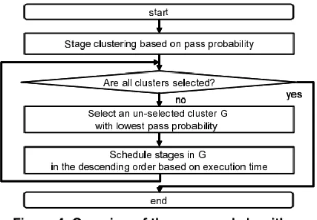
Table 1. Data for an example system. 1st stage 2nd stage 3rd stage core i timei,1 ppi,1 timei,2 ppi,2 timei,3 ppi,3
1 100 0.8 100 0.5 100 0.9
2 100 0.7 100 0.5 100 0.9
Then, by using the above equation, the probability Pf(t) is defined as follows. Here, we assume that Tf =
{t1,t2, ...,ti, ...}and ti<=ti+1(i.e., elements in Tf are sorted in the ascending order).
Pf(t1) = 1 −&
ck∈C
Pn f(t1,k) (7)
Pf(ti) =&
ck∈C
Pn f(ti−1,k) −&
ck∈C
Pn f(ti,k) for i ≥ 2 (8)
To illustrate the expected test time calculation, we use the test parameters shown in Table 1 for the test schedules shown in Figure 3. The test time is 600 for all three test schedules. In the core-based test scheduling shown in Fig- ure 3(a), the expected test time is 567 where the pass prob- ability for each core is set to ppi,1+(1 − ppi,1) · ppi,2·ppi,3. If we change the schedule unit from core to stage shown in Figure 3(b), the expected test time is 419.05. Furthermore, by considering that it is not necessary to execute the three stages of each core consecutively as long as they are exe- cuted in keep the order shown n Figure 3(c), the expected test time is reduced to 357.85.
5 Scheduling Algorithm
In this section, we describe an efficient and effective stage-based test scheduling method for memory cores with BISR scheme. When we consider the test scheduling prob- lem for memory cores with BISR scheme, the number of TAM wires is not the constraint but the total power con- sumption during test should be considered not to exceed a certain limit. Therefore, our objective is to minimize the expected test time under power constraints. Before describ- ing the proposed algorithm, we formally present the test scheduling problem PBISRas follows.
Definition 1 PBISR: Given the maximum power consump- tion Pmax, a set of cores C and for each core ci ∈ C the test parameters for each stage si, jincluding timei, j, poweri, j and ppi, j, determine a test schedule such that: (1) the total power consumption at any moment does not exceed Pmax, (2) the precedence constraints are satisfied (i.e., for each core ci, si,2must not start before si,1ends and si,3must not start before si,2ends) and (3) the overall expected test time is minimized.
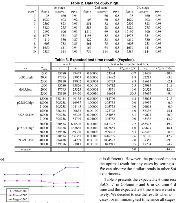
5.1 Proposed Scheduling Algorithm
An outline of the proposed algorithm is presented in Fig- ure 4. The above proposed algorithm is designed so that two important factors (1) pass probability and (2) execution
Figure 4. Overview of the proposed algorithm. time of each stage can be taken into consideration. First, the algorithm performs stage clustering based on its pass probability so that the stages in each cluster have similar pass probability (This step is explained in more detail in the sequel of this section). Then, it repeatedly selects an un- selected cluster with lowest pass probability, and decides test schedule for each stage in the selected cluster. In this step, we select an un-scheduled stage with longest execu- tion time (not lowest pass probability) such that the preced- ing stages are already scheduled. Then, we schedule it to the earliest time slot such that the power and precedence constraints are satisfied. This process is repeated until all stages in the cluster are scheduled.
Stage Clustering Procedure
In this step, we first calculate the fail probability f pi, j
for each stage si, j of core cias follows, and sort stages in the descending order based on its fail probability.
• f pi,1=0
• f pi,2=(1 − ppi,1) · (1 − ppi,2)
• f pi,3=(1 − ppi,1) · ppi,2·(1 − ppi,3)
Figure 5(a) shows an example of sorted stages. Then, let S be the set of all stages except 1st stages, and we calculate the variance VS of fail probabilities in S and the threshold variance Vthas follows.
VS=
'
si, j∈Sf pi, j2
|S| −
( 'si, j∈Sf pi, j
|S| )2
(9)
Vth= α·VS (10)
Here, α is a constant value and we used seven values (10, 1, 0.1, 0.01, 0.001, 0.0001, 0.00001) in our experiments.
After that, we create a group G1that consists of the stage with highest fail probability, and add the stage with next highest fail probability to G1if the variance VG1after adding it does not exceed Vth. This process is repeated until VG1
exceeds Vth. When VG1exceeds Vth, we create a new group G2and repeat the same procedure. Whenever the variance VGi of group Gi exceeds Vth, we create a new group and repeat the same procedure until all stages in S are clustered.
Figure 5. An example of the clustering procedure. Figure 5(b) shows an example of clustering process for 2nd and 3rd stages when Vthis 0.001.
Finally, 1st stage si,1of each core ciis added to the group where 2nd stage si,2of the core belongs in order to satisfy the precedence constraints in the following scheduling step. Figure 5(c) shows the final result of the stage clustering pro- cedure in the example.
The proposed algorithm can flexibly adjust the size of clusters by using the parameter α depending on the given problem instance. Therefore, if it is better to give the pri- ority to the execution time of each stage, then we can in- crease the size of clusters (decrease the number of cluster) in the stage clustering step and schedule the greater part of stages in the descending order based on its execution time in scheduling step. On the other hand, if we decrease the size of clusters, then, we can schedule the greater part of stages in the descending order based on its fail probability (we can give the priority to the fail probability).
6 Experimental Results
We obtained experimental results for the ITC’02 bench- marks [20]. As the original benchmark does not include test data for memory cores with BISR scheme, we have added those data ourselves. The test data we used in this experiments for d695 is shown in Table 2. We assume that all cores in the original benchmark are memory cores with BISR scheme. For each core ci, we used the test time when 16 bits TAM wires are assigned to ci as the execu- tion time of 1st and 3rd stage (i.e., timei,1and timei,3), and timei,2 = timei,1/10. We have used the power consump- tion shown in [7] as the power consumption for 1st and 3rd stages for d695. For p22810 and p93791, we used the sum- mation of the number of FFs in core ci as the power con- sumption for 1st and 3rd stages. We assume that the power consumption of 2nd stages is equal to poweri,1/10. We have used two different sets of pass probabilities within the range used in [18] for each benchmark. The first set is denoted as
“soc high” where the pass probabilities of 1st stages vary from 0.85 to 0.95. The second set is denoted as “soc low”
Table 2. Data for d695 high.
1st stage 2nd stage 3rd stage
core i timei,1 poweri,1 ppi,1 timei,2 poweri,2 ppi,2 timei,3 poweri,3 ppi,3
1 38 660 0.94 4 66 0.8 38 660 0.96
2 1029 602 0.92 103 60 0.8 1029 602 0.96
3 2507 823 0.95 251 82 0.8 2507 823 0.98
4 5829 275 0.91 583 28 0.8 5829 275 0.97
5 12192 690 0.93 1219 69 0.8 12192 690 0.98
6 11978 354 0.85 1198 35 0.8 11978 354 0.99
7 4219 530 0.87 422 53 0.8 4219 530 0.96
8 4605 753 0.85 461 75 0.8 4605 753 0.95
9 1659 641 0.94 166 64 0.8 1659 641 0.98
10 7586 1144 0.91 759 114 0.8 7586 1144 0.95
Table 3. Expected test time results (#cycles).
α=10 best α for expected test time
soc Pmax T E α Tm (Tm−T)/T Em (Em−E)/E
1500 53780 39439 0.10000 53394 -0.7 31409 -20.4
d695 high 2000 37795 23063 0.10000 38482 1.8 22213 -3.7
2500 28110 19002 0.00001 30723 9.3 18611 -2.1
1500 53780 35826 0.00100 56712 5.5 27985 -21.9
d695 low 2000 37795 23325 0.00001 43851 16.0 20523 -12.0
2500 28110 19450 0.00010 36624 30.3 17617 -9.4
15000 388434 169135 0.10000 412706 6.2 133095 -21.3
p22810 high 18000 305758 116957 1.00000 305758 0.0 116957 0.0
21000 305758 104143 1.00000 305758 0.0 104098 0.0
15000 388434 100832 0.00100 372798 -4.0 56336 -44.1
p22810 low 18000 305758 66326 0.01000 355057 16.1 49074 -26.0
21000 305758 52749 0.01000 305758 0.0 45436 -13.9
30000 1380574 600596 0.00010 1411397 2.2 485525 -19.2
p93791 high 40000 984478 463688 0.00010 1092855 11.0 379677 -18.1
50000 839856 359300 0.01000 909421 8.3 328442 -8.6
30000 1380574 206351 0.00010 1416285 2.6 180190 -12.7
p93791 low 40000 984478 194239 0.00100 1004597 2.0 137355 -29.3
50000 839856 123013 0.00100 843941 0.5 117234 -4.7
average 6.0 -14.9
Figure 6. Variation of expected test time forαin d695 high.
where the pass probabilities of 1st stages vary from 0.5 to 0.95. We set the pass probabilities of 2nd stages to 0.8 and the pass probabilities of 3rd stages vary from 0.95 to 0.99 for both two sets (i.e., “soc high” and “soc low”).
Figure 6 presents the variation of the expected test time according to α we used in the proposed heuristic algorithm to adjust the number of clusters for d695 high. We can see that there is no trend between α and the expected test time (depending on the given power constraint, the best value for
αis different). However, the proposed method can provide the optimal result for any cases by setting α appropriately. We can observe the similar trends in other SoCs used in our experiments.
Table 3 presents the expected test time results for the six SoCs. T in Column 3 and E in Column 4 denote the test time and the expected test time when we set α to 10, respec- tively. We decided to use the results when α = 10 as the best cases for minimizing test time since all stages belong to one cluster and only the execution time of each stage is taken into consideration during scheduling step when α = 10. From Column 5 to 9, we present the best expected test time among seven values for α (10, 1, 0.1, 0.01, 0.001, 0.0001, 0.00001). Column 5 denotes the value of α which gives the best expected test time. Columns 6 and 8 denote the test time Tmand the expected test time Emfor the α in Column 5. Column 7 and 9 denote the relative differences between Tand Tm, and between E and Em. We can see that the pro- posed method obtains savings in expected test time up to 44.1% by considering the pass probabilities using α. We can obtain 14.9% saving in expected test time on average while we lost only 6.0% in test time.
Table 4 shows the expected test time results for the two
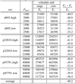
Table 4. Expected test time for two different sched- ule unit sizes (#cycles).
schedule unit stage core
soc Pmax Es Ec
Es−Ec Ec
1500 31409 53108 -40.9
d695 high 2000 22213 37001 -40.0
2500 18611 28830 -35.4
1500 27985 44546 -37.2
d695 low 2000 20523 31130 -34.1
2500 17617 26390 -33.2
15000 133095 254533 -47.7 p22810 high 18000 116957 200031 -41.5 21000 104098 191910 -45.8
15000 56336 85872 -34.4
p22810 low 18000 49074 81785 -40.0
21000 45436 69329 -34.5
30000 485525 803096 -46.6 p93791 high 40000 379677 665586 -49.9 50000 328442 558671 -52.4 30000 180190 239866 -33.7 p93791 low 40000 137355 192196 -39.9 50000 117234 163519 -36.4
average -40.2
different schedule units: (1) proposed stage-based schedul- ing and (2) core-based scheduling where we consider the three stages in each core as one core-unit, and test schedul- ing and expected test time calculation is done based on the core-unit. Es in Column 3 denotes the expected test time for stage-based test scheduling, Ecin Column 4 denotes the expected test time for core-based test scheduling. Column 5 denotes the relative differences between Esand Ec. We can see that the proposed method obtains savings in expected test time up to 52.4% and 40.2% saving on average.
7 Conclusion
We have introduced a model to compute the expected test time in the proposed abort-on-pass/fail test schedule en- vironment for memory cores with BISR function and pro- posed a power-constrained test scheduling method to mini- mize the expected test time. To the best of our knowledge, test scheduling problem for memory cores with BISR func- tion has been formulated and addressed for the first time in this paper. We have made experiments on six benchmarks where we showed a significant expected test time reduction compared to the core-based test scheduling method which minimizes the test time.
Acknowledgments
This work was supported in part by Japan Society for the Promotion of Science (JSPS) under Grants-in-Aid for Sci- entific Research B(2)(No. 15300018) and for Young Sci- entists(B)(No.18700046). The authors would like to thank Prof. Michiko Inoue, Dr. Satoshi Ohtake and members of Computer Design and Test Laboratory in Nara Institute of Science and Technology for their valuable comments.
References
[1] Y. Zorian, E. J. Marinissen, and S. Dey, “Testing embedded-core based system chips,” in Proc. Int. Test Conf., pp. 130–143, Oct. 1998. [2] “IEEE standard testability method for embedded core-based inte-
grated circuits.” IEEE Std 1500-2005, 2005.
[3] V. Iyengar, K. Chakrabarty, and E. J. Marinissen, “Test wrapper and test access mechanism co-optimization for system-on-chip,” Journal of Electronic Testing: Theory and Applications, vol. 18, pp. 213–230, Apr. 2002.
[4] S. K. Goel and E. J. Marinissen, “Effective and efficient test archi- tecture design for SOC,” in Proc. Int. Test Conf., pp. 529–538, Oct. 2002.
[5] Y. Huang, W. T. Cheng, C. C. Tsai, N. Mukherjee, O. Samman, Y. Zaidan, and S. M. Reddy, “Resource allocation and test schedul- ing for concurrent test of core-based SOC design,” in Proc. Asian Test Symp., pp. 265–270, Nov. 2001.
[6] V. Iyengar, K. Chakrabarty, and E. J. Marinissen, “On using rectangle packing for SOC wrapper/TAM co-optimization,” in Proc. VLSI Test Symp., pp. 253–258,, Apr. 2002.
[7] Y. Huang, N. Mukherjee, S. Reddy, C. Tsai, W. T. Cheng, O. Sam- man, P. Reuter, and Y. Zaidan, “Optimal core wrapper width selec- tion and SOC test scheduling based on 3-dimensional bin packing algorithm,” in Proc. Int. Test Conf., pp. 74–82, Oct. 2002.
[8] E. Larsson, K. Arvidsson, H. Fujiwara, and Z. Peng, “Efficient test solutions for core-based designs,” IEEE Trans. Computer-Aided De- sign, vol. 23, pp. 758–775, May 2004.
[9] T. Kawagoe, J. Ohtani, M. Niiro, T. Ooishi, M. Hamada, and H. Hi- daka, “Built-in self-repair analyzer (CRESTA) for embedded drams,” in Proc. Int. Test Conf., pp. 567–574, Oct. 2000.
[10] V. Schober, S. Paul, and O. Picot, “Memory built-in self-repair using redundant words,” in Proc. Int. Test Conf., pp. 995–1001, Oct. 2001. [11] J. F. Li, J. C. Yeh, R. F. Huang, and C. W. Wu, “A built-in self-repair design for rams with 2-d redundancy,” IEEE Trans. VLSI Systems, vol. 13, pp. 742–745, June 2005.
[12] Y. Zorian and S. Shoukourian, “Embedded-memory test and re- pair:infrastructure IP for SoC yield,” IEEE Design and Test of Com- puters, vol. 20, pp. 58–6, May/June 2003.
[13] R. C. Aitken, “A modular wrapper enabling high speed BIST and repair for small wide memories,” in Proc. Int. Test Conf., pp. 997– 1005, Oct. 2004.
[14] C. W. Wang, J. R. Huang, Y. F. Lin, K. L. Cheng, C. T. Huang, C. W. Wu, and Y. L. Lin, “Test scheduling of BISTed memory cores for SoC,” in Proc. Asian Test Symp., pp. 356–361, Nov. 2002. [15] W. Wang, “March based memory core test scheduling for SOC,” in
Proc. Asian Test Symp., pp. 248–253, Nov. 2004.
[16] M. Miyazaki, T. Yoneda, and H. Fujiwara, “A memory grouping method for sharing memory BIST logic,” in Asia and South Pacific Design Automation Conf., pp. 671–676, Jan. 2006.
[17] E. Larsson, J. Pouget, and Z. Peng, “Abort-on-fail based test schedul- ing,” Journal of Electronic Testing: Theory and Applications, vol. 21, pp. 651–658, Dec. 2005.
[18] U. Ingelsson, S. Goel, E. Larsson, and E. J. Marinissen, “Test scheduling for modular SOCs in an abort-on-fail environment,” in Proc. European Test Symp., pp. 8–13, May 2005.
[19] S. Bahukudumbi and K. Chakrabarty, “Defect-oriented and time- constrained wafer-level test length selection for core-based SOCs,” in Proc. Int. Test Conf., pp. 1–10, Oct. 2006.
[20] E. J. Marinissen, V. Iyengar, and K. Chakrabarty, “A set of bench- marks for modular testing of SOCs,” in Proc. Int. Test Conf., pp. 519– 528, Oct. 2002.