SPECTROSCOPIC STUDY OF SURFACE
TREATMENTS FOR Nb SRF CAVITY
Puneet Veer Tyagi
Supervised by
Dr. Shigeki Kato
Department of Accelerator Science School of High Energy Accelerator Science The Graduate University for Advanced Studies
2011 (School Year)
A Ph.D. Thesis
Spectroscopic Study of
Surface Treatments for Nb SRF Cavity
By
Puneet Veer Tyagi
SUPERVISOR CERTIFICATE
This is to certify that the thesis entitled “SPECTROSCOPIC STUDY OF SURFACE TREATMENTS FOR NB SRF CAVITY” describes the original work done by Puneet Veer Tyagi, under my supervision for the degree of Doctor of Philosophy of the Graduate University for Advanced Studies, Japan. Mr. Puneet Veer Tyagi has fulfilled the required formalities as per the university rules known to us.
Dr. Shigeki Kato Associate Professor
KEK/The Graduate University for Advanced Study Japan
THESIS DEDICATED
TO
MY FAMILY
Especially to my wife Payal
for her consistent encouragement through out my Doctoral course. She suffered a lot, staying alone in India but never complaint.
Everybody has difficult years, but a lot of times the difficult years end up being the greatest years of your whole entire life, if you survive them.
Brittany Murphy, Seventeen Magazine, September 2003
Contents
Supervision Certificate iii
Contents v
List of figures viii
List of Tables xii
Acknowledgments xiii
Abstract 1
Chapter 1
Introduction
31.1. International linear collider...5
1.2. Superconducting radio frequency cavity...7
1.2.1. RF cavity....7
1.2.2. Electromagnetic modes in a cavity...7
1.2.3. Accelerating field in a cavity...8
1.2.4. Energy stored and power dissipation in a cavity...8
1.2.5. Quality factor...8
1.2.6. Geometrical factor and shunt impedance...9
1.2.7. RF cavity with external coupling...9
1.2.8. Design consideration of a cavity...10
1.3. Cavity fabrication....11
1.3.1. Flow chart of a cavity fabrication from Nb mother material...11
1.3.2. Nb production...12
1.3.3. Nb ingots...12
1.3.4. Nb sheets...13
1.3.4.1. Residual resistance ratio (RRR)...14
1.3.5. Fabrication of cavity parts....15
1.3.6. Nine-cell cavity...16
1.3.6.1. Electron beam welding...17
1.3.7. Cavity inspection and tuning...18
1.3.8. Surface finishing and cleaning....18
1.3.8.1. Mechanical centrifugal barrel polishing (CBP)...18
1.3.8.2. Buffered chemical polishing...19
1.3.8.3. Electropolishing...20
1.3.8.4. Rinsing...21
1.4. Motivation and aim...23
1.5. References...24
Chapter 2
Experimental Setups
262.1. Surface analysis system...28
2.1.1. Main chamber for surface analysis...28
2.1.1.1. X-ray photoelectrons spectroscopy...29
2.1.1.1.1. Components of a XPS system....31
2.1.1.2. Secondary ion mass spectrometry...31
2.1.2.1. Components of a SIMS instrument...32
2.1.1.3. Auger electron spectroscopy...33
2.1.1.3.1. Components of a AES instrument...34
2.1.2. Vacuum system for surface analysis system...35
2.1.3. Three loadloack systems...35
2.1.4. Sample storage chamber...36
2.2. Vacuum suitcase and multiuse UHV system...37
2.3. Scanning electron microscope...38
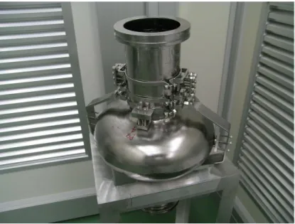
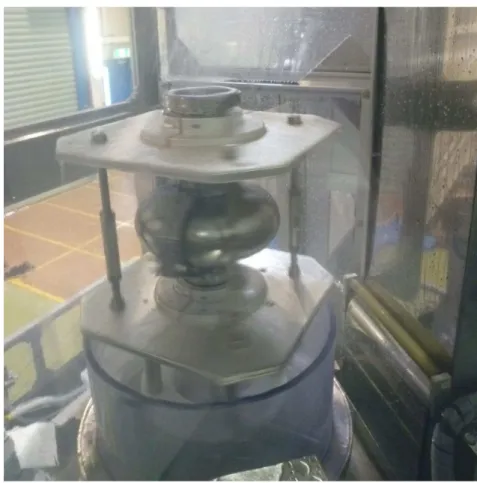
2.4. Electropolishing system...40
2.4.1. Laboratory electropolishing system...40
2.4.2. Cavity electropolishing system...41
2.5. Clean room...42
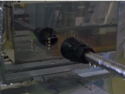
2.6. High pressure rinsing system...43
2.6.1. Laboratory high pressure rinsing system...43
2.6.2. Cavity high pressure rinsing system...43
2.7. Dry ice cleaning system...45
2.8. References...46
Chapter 3
E xperimental Procedures
473.1. Electropolishing experiments...49
3.1.1. Laboratory electropolishing...49
3.1.2. Test cavity electropolishing...50
3.2. High pressure rinsing experiments...53
3.2.1. Laboratory high pressure rinsing...53
3.2.2. Cavity high pressure rinsing...54
3.3. Dry ice cleaning experiments...55
3.4. Surface analysis procedure...56
Chapter 4
Experimental Results and Discussions
574.1. Electropolishing experimental results...59
4.1.1. Cavity EP...59
4.1.1.1. Cavity EP 1...59
4.1.1.2. Cavity EP 2...65
4.1.1.3. Cavity EP 3...70
4.1.2. Laboratory EP...74
4.2. High pressure rinsing experimental results...78
4.2.1. Cavity EP 4 and HPR...78
4.2.2. Laboratory HPR...82
4.3. Dry ice cleaning experimental results...89
4.4. References...92
Chapter 5
Conclusions
935.1 Conclusions of electropolishing experiments...95
5.1.1. Conclusions of cavity EP experiments...95
5.1.1.1. Conclusion of cavity EP 1 experiment...95
5.1.1.2. Conclusion of cavity EP 2 experiment...95
5.1.1.3. Conclusion of cavity EP 3 experiment...96
5.1.2. Conclusions of laboratory EP experiments...97
5.1.2.1. Conclusion of laboratory EP 1 experiment...97
5.1.2.2. Conclusion of laboratory EP 2 experiment...97
5.2. Conclusions of high pressure rinsing experiments...99
5.2.1. Conclusion of cavity EP 4 and HPR...99
5.2.2. Conclusion of lab HPR experiment...100
5.3. Conclusions of dry ice cleaning experiment...101
Appendixes
Table of the surface analysis system specifications... 102
Tables of specifications of X-ray source...102
Table of Ion gun operating parameters...103
Table of operating modes of electron energy analyzer...103
List of Figures
Figure 1.1 The baseline two tunnels design of ILC. 5
Figure 1.2 The schematic layout of 500GeV center of mass energy machine [1] 6 Figure 1.3 (a) An equivalent LCR circuit of rf cavity. (b) Simple lumped LC circuit
representing a rf cavity [1.4, 1.5]
7
Figure 1.4 (a) Schematic of EBM procedures. (b) Nb ingot during EBM [1.8]. 12 Figure 1.5 (a) The crucibles used in EBM. (b) Nb ingot produced after EBM [1.8]. 13 Figure 1.6 (a) The schematic of forging procedure containing Nb ingot in between. (b)
Forge machine
at ATI Wang company [1.8].
13
Figure 1.7 (a ) Cold rolling machine at ATI wang company. (b) Hot rolling machine at ATI Wang
company [1.8].
14
Figure 1.8 Molecules containing isolated quinoxaline and hole-transporting segments (n- and p-dopable)(a) Deep drawing of cavity. (b) The cups. (c) Mechanical shape measurement of cup. (d) RF measurement of dumbbell [1.8].
15-16
Figure 1.9 (a) Welded cavity parts. (b) Nine-cell cavity after welding [1.8]. 16-17 Figure 1.10 (a) Schematic view of an EBW machine. (b) The inside picture of an EBW
machine [1.8]. the dominance of p-doping character.
17 Figure 1.11 The plastic stones of different sizes for CBP. (a) New (b) used. 19
Figure 1.12 The schematic of a CBP process. 19
Figure 1.13 A Typical I-V characteristic curve for the EP [1.16]. 21 Figure 2.1 Surface analysis system connected with an UHV suitcase via three loadlock
chambers. It's base pressure is maintained of the order of 10-9 Pa.
28
Figure 2.2 The schematic view of a XPS system. 30
Figure 2.3 A typical XPS survey spectrum. 31
Figure 2.4 The schematic view of SIMS principle. 32
Figure 2.5 The typical SIMS mass spectrum. 32
Figure 2.6 (a), (b) : Schematic views of the Auger process. 33
Figure 2.7 A typical AES survey spectrum. 34
Figure 2.8 (Vacuum system for analysis system. (RGA : residual gas analyzer, EXG : extractor gauge, ITR 90 and 999 : combination gauges, CCG : cold cathode gauge, GV : gate valve, UV source : ultraviolet source).
35
Figure 2.9 (a) An UHV suitcase with carousel, (b) Multiuse UHV system. 37 Figure 2.10 The picture of the JSM 6500F scanning electron microscope. 38 Figure 2.11 (a) The laboratory EP system. The Nb plate with samples (anode) is attached
with movable shaft and two Al plates (cathodes) are dipped in the EP acid. (b) Control software of
the laboratory EP process.
40
Figure 2.12 The EP bed with a single cell cavity (the acid is circulated through the left to right side).
41 Figure 2.13 (a) The class 10 clean room, (b) A clean booth and (c) A clean bench. 42 Figure 2.14 The laboratory high pressure system. (a) The lance with the water gun and 43
(b) The Kranzle high pressure washer machine.
Figure 2.15 (a) The Cavity High Pressure system. (b) HPR control system. 44 Figure 2.16 (a) The DIC gun. (b) The CO2 cylinder connected with DIC gun. 45 Figure 3.1 (a) Nb base plate and (b) Nb samples mounted on the base plate. 49 Figure 3.2 (a) Sample cavity with six holes at "equator", "iris" and "beam pipe"
positions. (b) Disc type sample used for electropolishing.
50 Figure 3.3 The cavity assembled with six Nb disc type samples. 51 Figure 3.4 (a) Cu plated sample holder, (b) Sample sitting on the sample holder and (c)
Six sample carousel.
51 Figure 3.5 The Nb sample mounted on the base plate during the laboratory HPR
experiment.
53 Figure 3.6 The Nb cavity assembled with Nb disc type samples during the cavity HPR
experiment.
54
Figure 3.7 The dry ice cleaning of the Nb sample in air. 55
Figure 3.8 (a) Inner view of the main chamber. (b) Ideal raster and probing area of sample surface : top view and cross-sectional view.
56 Figure 4.1 Comparison of XPS spectra among equator, iris, and beam pipe samples
EPed in the cavity EP 1 experiment, (a) Nb spectrum, (b) Carbon spectrum, (c) Oxygen spectrum and (d) Sulfur spectrum
61
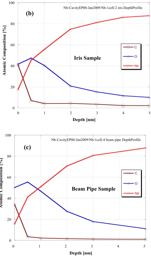
Figure 4.2 Depth profiles of the EPed samples in the cavity EP 1 experiment up to 5 nm, (a) Equator sample, (b) Iris Sample and (c) Beam pipe sample.
63 Figure 4.3 A typical SEM image of the beam pipe sample surface treated in cavity EP 1
experiment
64 Figure 4.4 Secondary ion images with a resolution of 256×256 pixels and a color
gradation in 40 steps linearly to the ion intensity of sulfur compound. The brightest dots in each image show sulfur concentrations and it's compounds locally concentrated with a size of around 20 μm
64
Figure 4.5 Comparison of XPS spectra among equator, iris, and beam pipe samples EPed in cavity EP 2 experiment, (a) Nb spectrum, (b) Carbon spectrum, (c) Oxygen spectrum, (d) Fluorine spectrum and (e) Sulfur spectrum.
67
Figure 4.6 Depth profiles of the EPed samples in the cavity EP 2 experiment up to 5 nm, (a) Equator sample, (b) Iris Sample and (c) Beam pipe sample.
69 Figure 4.7 A typical SEM image of the beam pipe sample surface treated in cavity EP 2
experiment.
69 Figure 4.8 Comparison of XPS spectra among equator, iris, and beam pipe samples
EPed in cavity EP 3 experiment, (a) Nb spectrum, (b) Carbon spectrum, (c) Oxygen spectrum, (d) Fluorine spectrum and (e) Sulfur spectrum.
72
Figure 4.9 Depth profiles of the EPed samples in the cavity EP 3 experiment up to 5 nm, (a) Equator sample, (b) Iris Sample and (c) Beam pipe sample.
74 Figure 4.10 Comparison of XPS spectra among samples treated in lab EP 1 and 2
experiments, (a) Nb spectrum, (b) Carbon spectrum, (c) Oxygen spectrum, (d) Fluorine spectrum and (e) Sulfur spectrum.
77
Figure 4.11 Comparison of XPS spectra among equator, iris, and beam pipe samples EPed in cavity EP 4 followed by HPR experiment, (a) Nb spectrum, (b) Carbon spectrum, (c) Oxygen spectrum, (d)
Fluorine spectrum and (e) Sulfur spectrum.
80
Figure 4.12 Depth profiles of the EPed samples in cavity EP 4 followed by HPR experiment up to 5 nm, (a) Equator sample, (b) Iris Sample and (c) Beam pipe sample.
82
Figure 4.13 Depth profile of the BCPed samples followed by UPW rinsing up to 5 nm. 83 Figure 4.14 Depth profiles of the BCPed samples followed by HPR experiment with 8
MPa up to 5 nm, (a) With a dose of 0.79 l/cm2and (b) With a dose of 7.9 l/cm2.
84
Figure 4.15 Depth profiles of the BCPed samples followed by HPR experiment with 10 MPa up to 5 nm, (a) With a dose of 0.79 l/cm2and (b) With a dose of 7.9 l/cm2.
86
Figure 4.16 Depth profiles of the BCPed samples followed by HPR experiment with 15 MPa up to 5 nm, (a) With a dose of 0.79 l/cm2 and (b) With a dose of 7.9 l/cm2.
87
Figure 4.17 (a) Variation of oxide layer FWHM as a function of pressure and dose. (b) Reduction in fluorine concentration based on pressure and dose.
88 Figure 4.18 The XPS spectra of sample surface after the DIC experiment in normal
environment. (a) Sulfur and (b) Fluorine.
90 Figure 4.19 The XPS spectra of sample surface after the DIC experiment in nitrogen
environment. (a) Sulfur and (b) Fluorine.
91
List of Tables
Table 1.1 The required design parameters for designing a cavity. 10 Table 1.2 Expected RRR contribution for 1 wt ppm impurities for Nb [1.8, 1.9]. 14-15 Table 2.1 Brief description of the analysis techniques installed in the main chamber. 29 Table 4.1 Summary of the experimental conditions of cavity EP experiments. 59 Table 4.2 The experimental conditions of cavity EP 1 experiment. 59 Table 4.3 Atomic percentages of the elements present on the samples surface after
cavity EP 1 experiment.
60 Table 4.4 The experimental conditions of cavity EP 2 experiment. 65 Table 4.5 Atomic percentages of the elements present on the samples surface after
cavity EP 2 experiment.
65 Table 4.6 The experimental conditions of cavity EP 3 experiment. 70 Table 4.7 Atomic percentages of the elements present on the samples surface after
cavity EP 3 experiment.
70 Table 4.8 Summary of the experimental conditions of Lab EP experiments. 74 Table 4.9 Atomic percentages of the elements present on the samples surface after
Laboratory EP experiments.
75 Table 4.10 The experimental conditions of cavity EP 4 experiment. 78 Table 4.11 Atomic percentages of the elements present on the samples surface after
cavity EP 4 experiment followed by HPR.
78 Table 4.12 The atomic composition present at top surface of the samples after HPR
with different pressures as a function of dose.
83
Table 4.13 The experimental conditions of DIC experiments. 89
Table 4.14 Atomic composition present at top surface after the DIC experiments in both the conditions.
89-90 Table 5.1 The summary of experimental results of the cavity EP experiments. 96 Table 5.2 The summary of experimental results of the laboratory EP experiments. 97 Table 5.3 The experimental results of the cavity EP 4 followed by the HPR
experiment.
99 Table 5.4 The experimental results of the BCP experiment followed by the HPR
with different pressures and doses.
100 Table 5.5 The experimental results of the DIC experiment in air and nitrogen. 101
Acknowledgments
Time goes by so fast. The last three years were highly eventful and every day presented new challenges and opportunities. This period has brought me valuable new experiences in both a scientific and personal perspective. Realizing the unique opportunity to obtain a Ph.D. degree would not have been possible without the contributions of many people.
Foremost, I would like to thank Dr. Shigeki Kato for my integration in his group and allowing me to work in a nice scientific environment as well as discussing many topics of vacuum science and surface science with me. He fearlessly accepted me as a PhD candidate and was the main creator of the great ideas, techniques and whole background of this thesis. We experienced together all the ups and downs of routine work, the shared happiness of success and the depression of failure. He managed to teach me how to work independently (which is very important), but at any time, his useful advice was available to me. These three years, I spent as a part of surface analysis laboratory proved to be very helpful for me in developing new scientific ideas and skills. I would like to thank you for your help and sharp views, which really improved the quality of the thesis. On the personal side, he did not hesitate to invite his students to become an extended part of his family, I appreciate this immensely.
I am very grateful to Dr. M. Nishiwaki who sets many things for me to start on my project. I gained a lot from her experience and expertise. I learned useful things from her on experimental side.
I am highly indebted to Dr. H. Hayano and Dr. T. Saeki for allowing me to work in STF and providing me their kind help and advices during the experiments.
I express my gratitude to Dr. M. Sawabe and all the technical staff of STF for their kind help in performing electropolishing and buffered chemical polishing experiments.
Two people with whom I enjoyed every moment in Tsukuba are Dr. Noguchi and Mr. Chouhan. They helped me in all spheres of life: during experiments as well as in daily life. I am fortunate to have colleagues like them. I also admire Mrs. Sonam Chouhan (wife of Mr. Vijay Chouhan), who cooked delicious food for me and invited many times for a nice food.
I would like to acknowledge the Japanese government (MEXT : Ministry of Education, Culture, Sports, Science and Technology) for financial support in the form of Monbukagakusho scholarship.
I am very thankful to Mr. Y. Aizawa, S. Hasegawa and other Sokendai staff for their valuable help in all administrative processes.
I am highly obliged to Ulvac-PHI for providing me the TOF-SIMS analysis of our cavity EP 1 sample and Applied Surface Technologies, USA for providing the dry ice cleaning equipment.
Also outside of science, there were people whose help and support was very important. I greatly admire my parents: Mr. Ajai Veer Singh Tyagi and Mrs. Sushila Tyagi. They have always encouraged me and supported me all the time from the joining of research program till today in every aspect. I also wish to express my feelings for my brother Dr. Vineet Veer Tyagi and sister in law Dr. Richa K. Tyagi for their full-fledged co-operation and inspiration. They are the ones who have always boosted my moral in carrying out my work. I also admire my niece Ananya, my little angel, who did not directly contributed to my thesis but gave me a lot of humor when talking to her. I forgot all the work stress when listening her childish talks and freshen myself.
Finally, I would like to mention the great love and care of my wife Dr. Payal Tyagi during the last year of my thesis. I can't simply express her contribution in words. She has helped me in every aspects like thesis modification, moral support etc. Without her love and care, it would have been difficult for me to achieve my goals. Above all, I thank almighty God for providing me strength, motivation and courage.
Abstract
The superconducting radio frequency (SRF) cavities are being used worldwide in particle accelerators to achieve a high energy beam of charged particles. These cavities are made of high purity niobium (Nb) material and work at 2 K temperature. The inner surface of these cavities plays the most important role in order to obtain good performances in terms of the high field gradient. Therefore, the surface treatments associated with SRF cavities are the key issues toward the achievement of the high field gradient larger than 35 MV/m during vertical test of the nine-cell cavity for International Linear Collider (ILC). In the recent years, extensive research has been done to enhance the cavity performance by applying improved surface treatments such as mechanical grinding, buffered chemical polishing (BCP), electropolishing (EP), electrochemical buffing (ECB), mechanochemical polishing (MCP), tumbling, etc., followed by various post-treatment methods such as ultrasonic pure water rinse, alcoholic rinse, high pressure water rinse (HPR), hydrogen per oxide rinse and baking etc. to obtain smooth and contaminant free surface.
Among all surface treatments, the EP followed by HPR seems to be the salient surface treatment method and used worldwide as a final surface treatment which provides the promising results. However, as a result of the EP process at laboratory level, some contaminants such as sulfur, fluorine, and carbon have been identified at the surface, which might be the sources of field emission when a high electric field is excited in a SRF cavity and limit the performance. Therefore it is of interest to characterize the status of surface after the EP process as well as see the effect of HPR with the help of surface analytical tools. The use of surface analytical tools will enable to find the optimum conditions of the surface treatments necessary for the mass production of efficient SRF cavities.
In this thesis, the efforts have been made to understand the behavior of EP inside a real cavity based on different EP conditions and see the effect of HPR with different pressures and doses. The total work can be summarized as follows :
(1) The theory and working principle of SRF cavities have been introduced. The manufacturing procedure, engineering and various surface treatment methods have been discussed in details. A wide literature survey has been done.
(2) The main experimental setups such as surface analytical system, scanning electron microscope, electropolishing system, HPR facility and clean room etc. have been introduced. The necessary systems for experiments such as three loadlock systems attached with surface analysis system, vacuum
suitcases, experimental setup to carried out lab-HPR experiments etc. were constructed.
(3) A series of cavity EP experiments by using a real Nb test cavity attached with six Nb disc type samples were carried out with different EP conditions in the same manner as ILC cavities are processed.
(4) The experimental results with high current density and aged EP acid solution showed a greater existence of sulfur and fluorine at the Nb surfaces in comparison of the experiment with fresh EP acid which confirms the sulfur generation is proportional to the aging of the EP acid solution. The chemical state of sulfur was confirmed as a mixture of SO4-- and SO3--.
(5) The experimental results with low current density demonstrated that the low current is quite helpful in order to mitigate the sulfur and fluorine at the Nb surfaces.
(6) Two laboratory EP experiments were also conducted with low and high current density. The experimental results were quite consistent with the cavity EP experiments and showed that low current density was very helpful in order to mitigate sulfur/sulfide from the surface.
(7) The HPR experiment was conducted on BCPed samples in order to demonstrate the effect of different pressures and doses which might be very helpful to optimize the HPR parameters. The thicker oxide layer was formed on Nb surface in proportional to high pressure and dose.
(8) The dry ice cleaning (DIC) was also tried on Nb samples after the lab EP. The results showed that the dry ice cleaning was not so effective in order to mitigate sulfur and fluorine form Nb surface while some hydrocarbons/dust particles were removed.
2
Chapter 1 Introduction
1.1. International Linear Collider
The International Linear Collider (ILC) will accelerate the electron and positron beams up to a center of mass energy of 500 GeV - 1 TeV [1.1, 1.2]. The electron - positron collision in the terascale energy region would explore the unknown regions of science. The International Technology Recommendation Panel (ITRP) committee for ICFA (International Committee for Future Accelerators) has decided to use superconducting radio frequency (SRF) technology for the accelerating structures (cavities). The tesla type nine-cell accelerating cavity is adopted as a baseline cavity for ILC. These cavities should provide a high accelerating E-field gradient individually in order to shorten the length of ILC. The goal of average accelerating E-field gradient in each cavity has been set to 35 MV/m in qualification test. The ILC will requires ~ 16000 SRF cavities with the operating accelerating E-field of 31.5 MV/m [1.2].
Fig. 1.1 : The baseline two tunnels design of ILC..
Figure 1.1 shows the two tunnels baseline design of the ILC accelerator in the Reference Design Report (RDR) in which one tunnel is proposed to use as a RF power source installation and supporting tunnel for the maintenance of the main tunnel. In the Technical Design Report (TDR), there will be changed to ILC baseline with single tunnel to reduce the construction cost of the ILC.
Fig. 1.2 : The schematic layout of 500GeV center of mass energy machine [1].
1.2. Superconducting Radio Frequency Cavity
1.2.1. RF Cavity : A space surrounded by the conducting walls in which infinite number of resonant electromagnetic modes can sustain is called a cavity. The cavities can be operated by the DC power or rf power depending upon the users choice. In order to accelerate charged particles, a cavity should provide an electric field E longitudinal with the velocity of charged particles. The magnetic field inside a cavity can provide deflection but can not accelerate the charged particles beam. The acceleration achieved by charged particles beam can be obtain by the Lorentz force equation [1.3]:
⃗a =q
(
E⃗+ ⃗V× ⃗B)
m(1.1) The cavities operated with the DC electric fields are able to provide the energies of only a few MeV and the higher energies can be achieved only by the transfer of energy from a rf resonant circuit. The energy can be transferred from a wave to a particle efficiently only when the cavity is tuned i.e. the cavity is excited at the same time of the charged particles passing through the cavity. The rf cavities work as a mode* transformer and an impedance# transformer during the excitation. A rf cavity can be considered as an equivalent of LCR circuit (fig 1.2 a, b) :
Fig. 1.3 : (a) An equivalent LCR circuit of rf cavity. (b) Simple lumped LC circuit representing a rf cavity [1.4, 1.5].
1.2.2. Electromagnetic Modes in a Cavity : The electromagnetic modes inside a cavity are given by the Maxwell's equations [3] :
(
∇2−c12∂ t∂22) {H⃗E⃗ }
=0 (1.2)
* Mode transformer (TEM TM), # Impedance transformer (low high) q
d
L R C d
(a) (b)
If there is no surface resistance at the cavity wall then Maxwell's equations satisfy the boundary conditions :
The tangential E field : ⃗n× ⃗E=0 (1.3) Normal magnetic field : ⃗n. ⃗E=0 (1.4) For a fixed shape, there is an infinite number of solutions for Maxwell's equations with sinusoidal time dependence. Assuming the solution of equation 1.2 is
~
e−iωtNow Maxwell's equations can be written as :
(
∇2−ω2c2
) {
⃗E
H⃗
}
=0 (1.5) where ω is the angular frequency of electromagnetic waves and c is velocity of light.From equation 1.5 it can be concluded that for an efficient acceleration we should choose a shape of cavity and mode where :
(1) The Electric field should be along the particle trajectory.
(2) There should not be any Magnetic field along the particle trajectory. (3) Velocity of the electromagnetic field and particle should be matched well.
1.2.3. Accelerating Field in a Cavity: Accelerating field (gradient) seen by the charged particles passing through a cavity can be written as [1.3-1.5]:
E⃗
acc=
1
L
∫
Ez(z)cos(ωz/ βc)dz (1.6) Where L=N λ2
is a reference length for the particles moving with the velocity of light.
1.2.4. Energy Stored and Power Dissipation in a Cavity : The total energy stored in a cavity at a time is give by [3-5]:
U=ε0
2
∫
dV(
E2
)
=μ02
∫
dV(
H2
)
(1.7) From equation 1.7, it can be concluded that the total energy is oscillating between electric and magnetic field because of sinusoidal time dependence of the field with a phase shift of 900.The total power dissipation in the cavity is given by : P= Rs
2
∫
da(
H∥)
2 (1.8)
Where Rs is the surface resistance of the cavity wall.
1.2.5. Quality Factor (Q0) : Quality factor is a measure of the performance of a cavity. It is given by the energy stored in a cavity divided by the energy lost in cavity walls because of surface
resistance of walls [1.4, 1.5].
Q0=ω0U Pdiss =ω
μ0 Rs
∫
dV(
H2)
∫
da(
H∥)
2 (1.9) 1.2.6. Geometrical Factor (G) and Shunt Impedance (Rsh) : The geometrical factor of a cavity is the product of quality factor and surface resistance of the cavity wall. It is basically shape and electric mode dependent quantity which is independent of the size (frequency), number of cells and the material of a cavity [4,5].G=QRs=2πη λ
∫
dV(
H2)
∫
da(
H∥)
2 (1.10) where η is the impedance of vacuum which is 377 Ω.The shunt impedance of a cavity depends on the mode geometry of the cavity and proportional to the number of cells in a cavity. The shunt impedance of a cavity can be written as :
Rsh= V
2c
2Pdiss
(1.11)
Where Vc is the accelerating voltage.
1.2.7. RF Cavity with External Coupling : In reality, the cavities are used with an external coupling to provide the power from a klystron to a charged particles beam. In such case :
The total power loss in a cavity is given by [1.4, 1.5] : Ptot=Pdiss+Pe (1.12) Where Pe is the power leaking out from the input coupler.
Similarly, the quality factor can be described as : QL=ω0 U
Ptot (1.13) and Qe=ω0 U
Pe (1.14) therefore 1
QL= 1 Q0+
1
Qe (1.15) Where QL is called as a loaded quality factor.
A coupling parameter can be defined as : β=Q0 Qe=
Pe
Pdiss (1.16) Now, QL can be written as : 1
QL= 1 +β
Q0 (1.17)
1.2.8. Design Consideration of a Cavity : To design a cavity following parameters are important to be considered [1.4-1.6].
Quantity Consideration
Critical field ( HS,max Eacc
) Minimum
Field emission ( ES,max Eacc
) Minimum
Shunt impedance, current loss ( 〈Hs2〉 Eacc2
) Minimum
Dielectric loss ( 〈Es2〉 Eacc2
) Minimum
Table 1.1 : The required design parameters for designing a cavity.
1.3. Cavity Fabrication
1.3.1. Flow Chart of a Cavity Fabrication from Nb Mother Material :
Nb Ingots Mother Material (Nb)
Pressing + Sintering + Electron Beam Melting (EBM, 2-3 times)
Electron Beam Welding (EBW)
High Purity Nb Sheets (RRR~300)
Fabrication of Cavity Parts and Pretuning
Vertical Test Various Surface Treatments +
Rinsing
Nine-Cell Cavity Cutting + Forging + Mechanical
Grinding+ Rolling
1.3.2. Nb Production : The mineral containing niobium (Nb) material is obtained from the mines. The Nb is then separated from the pyrochlore (NaCaNb2O6F) mineral. The mines containing pyrochlore mineral are mostly situated in Brazil. The separation of Nb from the pyrochlore ore is done in the following manners [1.7, 1.8]:
1. The pyrochlore ore is crushed and the magnetite is separated magnetically.
2. The ore is then chemically processed to give a concentrate ranging from 55 to about 60% niobium oxide (Nb2O5).
3. The mixture of Nb2O5 and aluminum powder are reacted to reduce the oxide to Nb. 4. The powder is pressed, sintered and electron beam melted to get the pure Nb ingots.
1.3.3. Nb Ingots : The sintered Nb is moved to the electron beam melting (EBM) facility to melt down. Figure 1.3 (a) and (b) show the schematic of an EBM and EBM of sintered Nb respectively [1.8, 1.9].
Fig. 1.4 (a) Schematic of EBM procedures. (b) Nb ingot during EBM [1.8].
A typical EBM machine contains a vacuum chamber and electron guns. The electrode (which is to be melted, sintered Nb in this case) is rotated during the melting. The electron beams are focused by using the focusing coils on to the material (sintered Nb) to be melted. The Nb drops are then fallen down in a molten pool on the ingot and is passed to a water cooled copper cylinder. During the meltdown of Nb, all the impurities are evaporated and pumped out by using a vacuum pump. The
(a) (b)
Vacuum Electron Guns
Electrode (rotating)
Ingot
Molten Pool Water Cooled
Crucibles
Focus & Aiming Coils
Electron Beams
ingot formed during the melting of Nb is continuously withdrawn and the rate of withdrawn should be carefully adjusted with the rate of material to insure proper outgassing and complete melting of the material. After getting Nb ingots this process is repeated 3-4 times (EB refining) to get the high purity Nb ingots.
Fig. 1.5 : (a) The crucibles used in EBM. (b) Nb ingot produced after EBM [1.8].
1.3.4. Nb Sheets : The high purity Nb sheets are prepared from the Nb ingots. To produce a sheet from Nb ingot, the Nb ingots are first forged and then moved to a rolling machine. The forging dies of 1500-2000 ton are used for forging [1.8, 1.9].
Fig .1.6 (a) The schematic of forging procedure containing Nb ingot in between. (b) Forge machine at ATI Wang company [1.8].
The forged Nb blocks are then moved to a rolling machine where the Nb sheets are prepared. There are two types of rolling methods : hot rolling and cold rolling can be used for rolling depending upon choice. If the temperature during rolling is maintained above the crystallization temperature of
(a) (b)
(b) (a)
Nb then it is called as a hot rolling and if temperature is lower than the crystallization temperature of Nb then it is called as a cold rolling.
Fig. 1.7 : (a ) Cold rolling machine at ATI wang company. (b) Hot rolling machine at ATI Wang company [1.8].
The top surface of Nb sheets is much damaged during the fabrication. The Nb sheets are then polished to remove the damaged layer of the surface. The defects such as point defects, interstitial, line dislocation etc. are then recovered by annealing (recrystallization) at 800 0C. The RRR measurement (purity check) of a Nb sheet is done after the recrystallization.
1.3.4.1. Residual Resistance Ratio (RRR) : In order to check the purity of the Nb sheets, the RRR measurement is carried out. The ratio of electrical resistivity of a metal at a normal temperature to the critical temperature (Tc) is called the residual resistance ratio (RRR). The impurities present in metals affect the electrical resistivity of the metals which lower the RRR value [1.8, 1.9].
RRR= ρ(295 K)
ρ(4 . 2K) (1.18) If there are some known impurities present in the metal then equation 1.18 can be written as : RRR=
ρ(295 K) ρ(4 . 2K)+
∑
i
∂ ρi
∂CiCi
(1.19)
where Ci is thermal conductivity of impurities.
Following table (1.2) gives the expected RRR contribution for 1 wt ppm impurities for Nb :
Element RRR Contribution
H 2640
N 4230
(a) (b)
C 4380
O 5580
Ti 53700
Zr 102000-239000
Hf 200000
W 261000-721000
Mo 717000
Ta 1149000
Table 1.2 : Expected RRR contribution for 1 wt ppm impurities for Nb [1.8, 1.9].
1.3.5. Fabrication of Cavity Parts : The fabrication of cavity parts can be summarized in following steps :
1. Deep drawing with hydraulic press is made and cups are prepared.
2. The mechanical measurement of cups are done in order to check the shape of the cups. 3. The cups are cleaned by ultra sonic cleaning and rinsing.
4. The iris region is trimmed and cups are reshaped if needed. 5. The trimmed cups are then cleaned once again.
6. The rf measurement of cups is performed to check the size and length of cavity by measuring frequency of resonance.
(a) (b)
Fig. 1.8 : (a) Deep drawing of cavity. (b) The cups. (c) Mechanical shape measurement of cup. (d) RF measurement of dumbbell [1.8].
1.3.6. Nine-Cell Cavity : All the cavity parts are cleaned very well and buffered chemical polishing (BCP) followed by rinsing is done prior to weld them. The cleaned cavity parts are moved to electron beam welding (EBW) facility and sequentially welded. After welding of iris and stiffening rings, the mechanical measurement and rf measurement of the dumb-bells are performed and dumb- bells are reshaped if needed. After reshaping of the dumb-bells, the dumb-bells are trimmed (equator regions) and chemically etched (BCP, 20-40 μm) followed by rinsing. The inner surface of the dumb-bell is visually checked and local grinding is done if needed. Then after, the equator regions are welded by using an EBW.
(c) (d)
(a)
Fig. 1.9 : (a) Welded cavity parts. (b) Nine-cell cavity after welding [1.8].
1.3.6.1. Electron Beam Welding : In order to avoid the contaminations during welding of the cavity parts, electron beam welding (EBW) is used. The EBW is operated under good vacuum in the range of 10-3 Pa. The welding is overlapped at the end of welding to avoid accumulation of impurities and wait to cool down before opening the chamber.
Fig. 1.10 : (a) Schematic view of an EBW machine. (b) The inside picture of an EBW machine [1.8].
(b)
(a) (b)
The welding sequence can be given as following : 1. Two cups are welded to form a dumb bell. 2. Stiffening ring is welded at the iris.
3. Two dumb-bells are welded together at equator position to form a single cell cavity. 4. More dumb-bells are added one by one.
5. End groups are added in the end.
6. For the mass production, welding of all dumb bells is done.
1.3.7. Cavity Inspection and Tuning : After the fabrication, all the cells are inspected and tuned. The eccentricity measurement of all the cells is done to ascertain the center of each cell, the inner surface is then inspected to ensure that there is no surface damages and field profile measurement (to check the frequency shift) is also performed in order to tune a cavity. Small mechanical adjustments are made to get the flat field and desired frequency.
1.3.8. Surface Finishing and Cleaning : Many contaminants and impurities are introduced at top surface of cavities and the surface layer is damaged during the deep drawing and EBW. In order to achieve a good performance of the cavities, removal of damaged surface layer and the impurities incurred during the fabrication is necessary. There are various surface treatment processes such as mechanical centrifugal barrel polishing (CBP), buffered chemical polishing (BCP), electropolishing (EP), electrochemical buffing (ECB), mechanochemical polishing (MCP) followed by various rinsing procedures are applied to the cavities. The ultrasonic degreasing in detergent is done in advance for all the cavities to remove grease, oil, finger prints from the surface before applying any of the surface treatments [1.9-1.13].
1.3.8.1. Mechanical Centrifugal Barrel Polishing (CBP) : The CBP was developed in KEK in 2001. It is a simple and easy polishing method but a very slow (removal rate ~5 μm/hr.) process. In CBP, the plastic stones and an abrasive liquid is added inside the cavity and cavity is rotated [1.9- 1.11]. Because of the rotation of cavity, these plastic particles are rubbing the cavity surface and hence material is removed resulting in a finished surface.
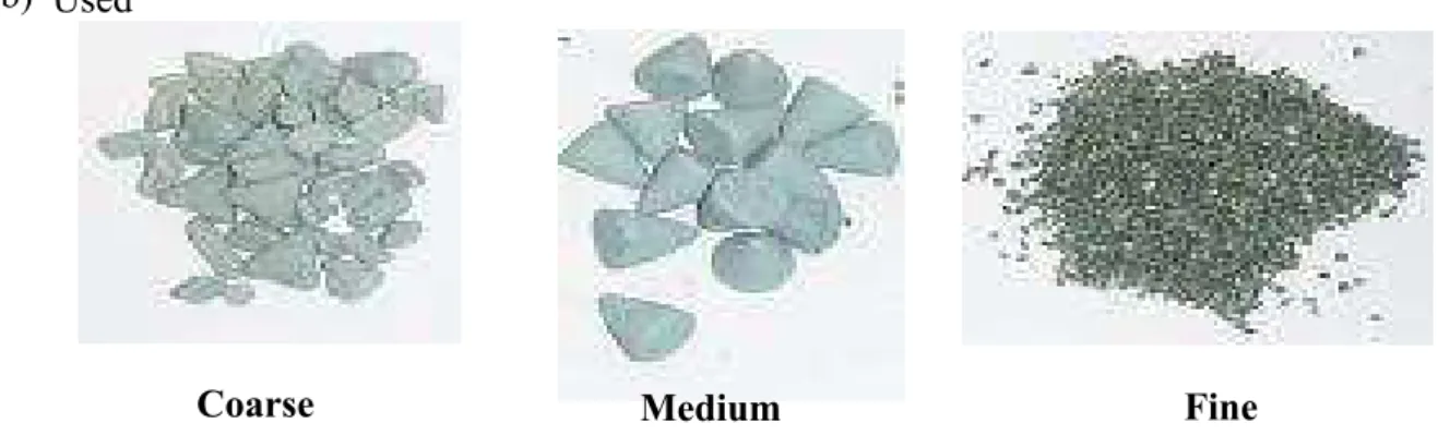
Coarse Medium Fine
(a) New
Fig. 1.11 : The plastic stones of different sizes for CBP. (a) New (b) used.
The surface roughness depends on the plastic stones size. For the bulk removal large particles are used. The removal rate also depends on particle size as well as rotation speed.
Fig. 1.12 : The schematic of a CBP process.
1.3.8.2. Buffered Chemical Polishing : The cavity requires interior chemistry to remove the damaged layer during welding and exterior chemistry to remove the oxide layer. The chemical etching is used to remove the oxide layer of surface which comes from fabrication steps of the cavity. The BCP is one of the chemical treatments widely used for cavity surface treatment and gives fairly good surface smoothness. The BCP electrolyte contains a mixture of hydrofluoric acid (HF, 49 wt%), nitric acid (HNO3, 69.5 wt%) and ortho-phosphoric acid (H3PO4, 85 wt%) in the ratio of 1 : 1 : 1 or 1 : 1 : 2 by volume respectively. The chemistry of BCP can be written as following [1.13-1.15]:
Coarse Medium Fine
(b) Used
Oxidation :
NO3- + 4 H+ + 3 e- NO + 2 H2O (1.20)
2 Nb + 5 H2O Nb2O5 + 10 e- + 10 H+ (1.21)
6 Nb + 10 HNO3 3 Nb2O5 + 10 NO + 5 H2O (1.22)
Reduction :
Nb2O5 + 14 HF 2 H6NbO2F7 + H2O (1.23)
Nb2O5 + 12 HF 2 HNbF6 + 5 H2O (1.24)
Nb2O5 + 10 HF 2 NbF5 + 5 H2O (1.25)
Nb2O5 + 10 HF 2 H2NbOF5 + 3 H2O (1.26)
HNbF6 + HF H2NbF7 (1.27)
The BCP reaction is an exothermic reaction therefore we need to control temperature very well during the reaction. The phosphoric acid is used as a buffer to slow the reaction rate. The typical etch rate is ~ 8 μm/min with mixture of 1 : 1 : 1 which is used for cavity subcomponents and ~3 μm/min for the mixture of 1 : 1 : 2. The etching rate is depending on the position also which is higher (2X) at an iris than an equator as well as a temperature gradient from one end to another end. The usual acid temperature during BCP is maintained at 10 - 15 0C to control the reaction rate and avoid the hydrogen absorption. The typical surface roughness after BCP is of the order of few micrometers (2-5 μm).
1.3.8.3. Electropolishing : These days EP is commonly used as a final surface treatment of SRF cavity as it gives much smother surface than BCP. The EP is an electrochemical process in which the typical mixture of hydrofluoric acid (HF, 40 wt%) and sulfuric acid (H2SO4, 96 wt%) in a volumetric ratio of 1 : 9 is used as an electrolyte. The cathode, made of aluminum is a long rod which is inserted from one end of the cavity and the Nb cavity itself works as an anode and a voltage is applied between these two electrodes. The anodization of Nb in H2SO4 results in the growth of Nb2O5 and F- ions from HF dissolves Nb2O5 which gives a current flow through the electrolyte. The basic reactions can be written as following [1.15-1.18]:
Oxidation :
2 Nb + 5 SO42- + 5 H2O Nb2O5 + 10 H+ + 5 SO42- + 10 e- (1.28) Reduction (hydrogen formation at an aluminum cathode) :
2 H+ + 2 e- H2 (1.29)
Oxido-reduction :
2 Nb + 5 H2O 5 H2 + Nb2O5 (1.30)
The Nb2O5 is dissolved in HF and niobium fluoride, oxofluoride (from equation 1.23 to 1.27) are formed. The fluorosulfate or oxysulfate and pyrosulfuryfluoride are made with sulfuric acid as sulfuric acid is considered as hydrated sulfur trioxide (SO3, H2O).
NbF5 + 2 (SO3, H2O) NbF3(SO3F)2 + 2 H2O (1.31) 2 NbF5 + 14 SO3 Nb2O(SO4)4 + S2O5F2 (1.32) The typical I-V characteristic of an EP process is given by fig. 1.12. The region AB : concentration polarization occurs and Nb is diluted, BC : instability, CD : after formation of viscous layer on Nb surface current density is limited (this region is the best condition for EP) and DE : additional cathodic process such as oxygen generation occurs. The voltage limitation in a plateau region (CD) depends on the diffusion coefficient of the viscous layer.
Fig. 1.13 : A Typical I-V characteristic curve for the EP [1.16].
The EP is an exothermic reaction and hence temperature is raised during EP which leads rise in current density. The Current density also depends on HF/H2SO4 ratio and decreases linearly with the lower ratio. Therefore, to achieve the best EP conditions we need to get a balance between all the EP parameters such as the electrolyte ratio, applied voltage to the anode, temperature etc. The current oscillations are also observed during the EP process because of dynamic balance between oxide formation and dissolution of Nb. The current oscillations are the indication of a good process i.e. the good balance of EP parameters. Typical etch rate by the EP process is maintained at 0.3 μm/min and surface roughness after the EP is of the order of 0.5 - 1 μm.
1.3.8.4. Rinsing : After the surface treatments of Nb cavities, some chemical residues such as sulfur, fluorine from the etching acids and dust particles are attached on the surface which are a hurdle in achievement of the high accelerating gradient (Eacc) and high Q0 value of the SRF cavities. Therefore post-polishing processes of inner surface has a great role in achievement of good
J (A /c m
2)
V
A
B
C D
E
performances of the SRF cavities. To remove these contaminants from the cavity inner surface, various rinsing processes such as ultra pure water rinse, ultrasonic pure water rinse, alcoholic rinse, detergent rinse, high pressure water rinse (HPR) with ultra pure water, dry ice cleaning have been used. After the rinsing cavities are assembled in clean room and moved to vertical test facility for vertical test [1.19-1.21].
1.4. Motivation and Aim
The performance of Nb SRF cavities is mainly limited by the following four factors : 1. Surface residual resistance.
2. Multipacting. 3. Field Emission. 4. Quench.
Among all the four limiting factors, the field emission depends on the contaminants present at the inner surface of the cavities. As it's described before, there are many steps involved in the fabrication of a cavity therefore the chances of inclusion of the contaminants are greatly enhanced. These contaminants are necessary to be removed in order to obtain good performances of the SRF cavities in terms of the achievement of high field gradient, hence the final surface treatment of SRF cavities is required. Although the good performances have been obtained lately by using EP followed by various post EP treatments, still much research and efforts are required to improve the processes to get consistently good results for the mass production. Some surface studies [1.21, 1.22] on Nb surface after the surface treatments have been done in the past, however surface study concerning contaminants present at the surface as a result of the surface processing have not been done so far. Therefore it is of interest to investigate the Nb surface and identify the chemical compositions present at the surface after the surface processing with different conditions.
In this thesis, the great efforts will be made to understand the behavior of surface treatments inside a real Nb cavity in order to obtain a very smooth and clean surface necessary for the mass production. The surface analytical tools such as x-ray photoelectron spectroscopy, secondary ion mass spectroscopy and scanning electron microscope etc. will be employed for the surface characterization after the surface treatments. The aim of our work is to find causes of low performances of Nb SRF cavities and optimum conditions for the surface processing to get an ultra smooth and clean surface. The use of optimum conditions will enhance the mass production with reduced cost.
1.5. References
[1.1] The International Linear Collider : Global design effort baseline configuration document. [1.2] Barry Barish "Introduction to the ILC : Lecture I-1, I-2", linear collider school, Villars-sur- Ollon, Switzerland, 25 Oct.-5 Nov. 2010.
[1.3] David J. Griffiths, "Introduction to Electrodynamics", Addison Wesley.
[1.4] Hasan Padmsee et al. "Handbook of rf superconductivity for Accelerators" John Wiley & Sons.
[1.5] Jean Delayen "Lecture on fundamentals of superconductivity, surface resistance, rf and cavities, microphonics", linear collider school, Villars-sur-Ollon, Switzerland, 25 Oct.-5 Nov. 2010.
[1.6] Jean Delayen "Lecture on Cavity design", linear collider school, Villars-sur-Ollon, Switzerland, 25 Oct.-5 Nov. 2010.
[1.7] Jean Delayen "Lecture,4 on cavity fabrication", linear collider school, Villars-sur-Ollon, Switzerland, 25 Oct.-5 Nov. 2010.
[1.8] Hiroaki Umezawa " Impurities analysis of high purity niobium in industrial production" Matériaux et techniques, 91(2003), 33.
[1.9] Jean Delayen "Lecture on surface preparation", linear collider school, Villars-sur-Ollon, Switzerland, 25 Oct.-5 Nov. 2010.
[1.10] G. Issarovitch et al "Development of centrifugal barrel polishing for treatment of superconducting cavities", Pproc. of SRF 2003, travemünde/lübeck, germany.
[1.11] CA Cooper and LD Cooley "Mirror smooth superconducting RF cavities by mechanical polishing with minimal acid use" FERMILAB-PUB-11-032-TD.
[1.12] P. A. Jacquet "electrolytic method for obtaining bright copper surfaces", Nature(London), 135, 1076 (1935).
[1.13] C. Boffo et. al. "Optimization of the BCP Processing of Elliptical Nb SRF Cavities", Proc. of the COMSOL Users Conference, 2006, Italy.
[1.14] A. Aspart and C.Z. Antoine "Study of the chemical behavior of hydrofluroic, nitric and sulfuric acids mixtures applied to niobium polishing", Applied surface science, 227(2004), 17. [1.15] Srinivas Bhashyam "Comparison of electropolishing and buffered chemical polishing – a literature review" td-03-046 report for fermi lab.
[1.16] F. Eozenou et. al., “Electropolishing of niobium: best EP parameters”, WP 5.1.1.4, Care report-06-010-SRF.
[1.17] K. Saito, “Development of electropolishing technology for superconducting cavities”, Proc. of PAC 2003, Portland, U.S.A.
[1.18] A. Aspert et. al., “Aluminum and sulfur impurities in electropolishing baths”, Physica C, 441(2006), 249.
[1.19] D. Sertore et. al., “Study of the high pressure rinsing water jet interactions", Proc. of EPAC08, Genoa, Italy
[1.20] TESLA Technology Collaboration, “Final surface preparation for superconducting cavities”, TTC-Report 2008-05.
[1.21] E. Cavaliere et. al., “High Pressure Rinsing Parameters Measurements”, Physica C 441 (2006), 254.
[1.22] Hui Tian et. al., “Surface studies of niobium chemically polished under conditions for superconducting radio frequency (SRF) cavity production”, applied surface science 253 (2006), 1236.
Chapter 2 Experimental Setups
2.1. Surface Analysis System
To characterize the surface condition and elemental composition present after the surface treatments, a surface analysis system (fig. 2.1) was used [2.1]. The surface analysis system is consist of a main chamber, the three loadlock systems and a sample storage chamber. The system is maintained at extremely high vacuum (XHV).
Fig. 2.1 : Surface analysis system connected with an UHV suitcase via three loadlock chambers. It's base pressure is maintained of the order of 10-9Pa.
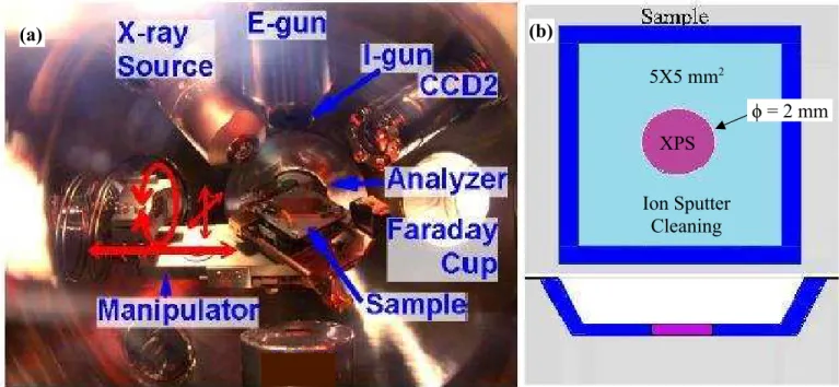
2.1.1. Main Chamber for Surface Analysis : The main chamber consists of an electron energy analyzer, an ion mass spectrometer, a x-ray source, an electron gun, an ion gun for depth profiling, an extractor gauge, a sample manipulator and a residual gas analyzer. The analysis system (fig 2.1) is capable of executing Auger electron spectroscopy (AES), secondary ion mass spectrometry (SIMS) with argon ion etching and XPS with probing area of 2 mm. Table 2.1 summarizes the details about analysis techniques.
Technique End-use Pros. Cons. X-ray photoelectron
spectroscopy (XPS)
Analysis of the binding energy of emitted photo electrons by the irradiation of Al/Mg x- rays on samples
.
Quantification is relatively easy.
It doesn't damage the sample's surface after the analysis.
It gives the information about the chemical state of elements present at the surface.
lateral resolution is not that good except micro- XPSSecondary ion mass spectrometry
(SIMS)
Investigation of the mass of secondary ions generated by the argon ion sputtering on samples
.
Sensitivity is very high.
Sputtering is necessary therefore surface is damaged specially in case of the dynamics SIMS analysis.
Quantification is difficult due to thesensitive ion probabilities to many sample
properties Auger electron
spectroscopy (AES)
Analysis of the kinetic energy of emitted auger electrons by the irradiation of e-beam on samples
.
Lateral resolution is good.
Sensitivity is high.
Signal to noise ratio is sometimes very weak.
Long time exposure to e-beam and high e- current damages the sample's surfaceTable 2.1 : Brief description of the analysis techniques installed in the main chamber.
2.1.1.1 X-ray Photoelectron Spectroscopy : The X-ray photoelectron spectroscopy (XPS) is a quantitative spectroscopic technique which measures the elemental composition, empirical formula, chemical state and electronic state of the elements present at top surface
of a material [2.2-2.4]. When a sample surface is irradiated by the soft X-rays photons (1-2 keV), the X-ray excitation of inner shell electrons of the target atoms induces direct emission of photoelectrons. These photoelectrons are then collected and passed through an
electron analyzer to a detector where the kinetic energy of these photoelectrons is measured. The kinetic energy of these photoelectrons is the characteristic of an element and hence provides the valuable information about the chemical composition present at top 1-10 nm of the material. The peak position and the peak area in a XPS spectrum are used to identify and evaluate the total relative atomic composition present on the surface. The peak shape gives unique information about the chemical shifts or chemical bonds of the elements.
Fig. 2.2 : The schematic view of a XPS system.
A typical XPS spectrum is the plot of binding energy of photoelectrons versus electrons count/number of electrons and the electron binding energy of each of the emitted electrons can be determined by using an equation that is based on the work of Ernest Rutherford (1914):
E(binding)=E(photon)−(E(kinetic )+Φ) (2.1) where Ebinding is the binding energy (BE) of the electron, Ephoton is the energy of X-ray photons being used, Ekinetic is the kinetic energy of the electron as measured by the instrument and Ф is the work function of the spectrometer used (not of the material).
Photo-Emitted Electrons (<1.5 keV) Escape only from the very top surface
(70-110 A) of the sample
Focused Beam of X-rays (1.5 keV)
Electron Collection
Lens
Electron Energy Analyzer (0-1.5 keV) (measures kinetic energy of electrons)
Electron Detector (Counts the electrons)
Electrons Take-off Angel
Samples are usually solid because XPS requires ultra high vacuum (<107 Pa) SiO2 / Si
Sample
Si (2p) XPS signals From a Silicon Wafer
Si (2p)
Fig. 2.3 : A typical XPS survey spectrum.
2.1.1.1.1. Components of a XPS System : The main components of a XPS system include : 1. A source of X-rays (usually Al or Mg).
2. An ultra-high vacuum (UHV) stainless steel chamber with UHV pumps. 3. An electron collection lens.
4. An electron energy analyzer. 5. An electron detector system.
6. A complementary sample introduction vacuum chamber (loadlock system). 7. A sample stage.
8. A set of stage manipulators.
2.1.1.2. Secondary Ion Mass Spectrometry : Secondary ion mass spectrometry (SIMS) is a surface analytical technique used in materials science and surface science to analyze the elemental composition of solid surfaces and thin films based on their atomic mass. The SIMS uses sputtering of the sample surface to get their atomic composition [2.2-2.4]. The sample surface is sputtered by a focused primary ion beam and secondary ions are ejected from the surface as a result of sputtering. These secondary ions are collected and analyzed by a mass spectrometer which measures the mass to charge ratio of each ion and determines the elemental, isotopic, or molecular composition of the surface.
Fig. 2.4 : The schematic view of SIMS principle.
The SIMS sensitivity is very high and able to detect elements present in the parts per billion ranges. A typical SIMS spectrum which is the plot of secondary the ions intensity versus ion mass number consists of two mass spectra of positive ions and negative ions.
Fig. 2.5 : The typical SIMS mass spectrum.
2.1.1.2.1 Components of a SIMS Instrument : Following are the main components of a SIMS instrument :
1. Primary ion gun (generating the primary ion beam).
2. Primary ion column, for accelerating and focusing the beam onto the sample.
3. A stainless steel ultra high vacuum chamber with UHV pumps.
4. A complementary attached vacuum chamber for sample introduction (loadlock system). 5. A sample stage with manipulators.
6. A secondary ion extraction lens followed by mass analyzer separating the ions according to their mass to charge ratio.
7. An Ion detection unit.
2.1.1.3. Auger Electron Spectroscopy : The Auger electron spectroscopy (AES) utilizes the emission of low energy electrons in the Auger process for determining the composition of the surface layers of a sample [2.2-2.4]. The Auger effect is an electronic process resulting from the inter- and intrastate transitions of electrons in an excited atom. When an atom is bombarded by a photon beam or a beam of electrons with the energies in the range of 2 keV to 50 keV, a core state electron can be removed and a hole is created. As this is an unstable state, the core hole can be filled by an outer shell electron, in which the electron moving to the lower energy level loses an amount of energy equal to the difference in orbital energies. This transition energy can be coupled to a second outer shell electron resulting the emission of secondary electron (Auger electron) from the atom if the transferred energy is greater than the orbital binding energy. The kinetic energy of the emitted electron can be given by :
E(kinetic)=E(corestate)−E(binding)−E(C) (1.34) where ECoreState, Ebinding and EC are respectively the core level, first outer shell and second outer shell electron energies, measured from the vacuum level. Figure 2.6 illustrates two schematic views of the Auger process.
Fig. 2.6 (a), (b) : Schematic views of the Auger process.
A typical AES spectrum (fig 2.7) is the plot of kinetic energy of auger electrons versus electron count/number of electron. The peak intensity gives the quantification information of element present on the surface.
Fig. 2.7 : A typical AES survey spectrum.
2.1.1.3.1: Components of an AES Instrument : An AES system requires the following components :
1. A Primary electron gun.
2. An ultra-high vacuum (UHV) stainless steel chamber with UHV pumps. 3. An electron collection lens.
4. An electron energy analyzer. 5. An electron detector system.
6. A complementary vacuum chamber for sample transfer (loadlock system). 7. Sample mounts and a sample stage.
8. A set of stage manipulators.
2.1.2. Vacuum System for Surface Analysis System :
In order to achieve XHV in the main chamber, a titanium sublimation pump (TSP) and two turbo molecular pumps (TMPs) in sequence are used. Each loadlock chamber contains one TMP and the sample storage chamber is equipped with one ion pump. Figure 2.8 shows the schematic of vacuum system of the analysis system.
Fig. 2.8 : Vacuum system for analysis system. (RGA : residual gas analyzer, EXG : extractor gauge, ITR 90 and 999 : combination gauges, CCG : cold cathode gauge, GV : gate valve, UV source : ultraviolet source).
2.1.3. Three Loadlock Systems : The analysis chamber can be connected to an UHV suitcase (section 2.2) via three loadlock chambers. The sample can be transferred from suitcase to the analysis chamber with the help of these three loadlock systems without exposing them in to the air. The mechanism of transferring the sample from suitcase to the main chamber through the loadlock systems is follows :
1. At first, the suitcase is connected to loadlock 3 (LL3) chamber and waiting until UHV is achieved.
![Fig. 1.2 : The schematic layout of 500GeV center of mass energy machine [1].](https://thumb-ap.123doks.com/thumbv2/123deta/6152465.102924/20.892.320.586.86.1073/fig-schematic-layout-gev-center-mass-energy-machine.webp)
![Table 1.2 : Expected RRR contribution for 1 wt ppm impurities for Nb [1.8, 1.9].](https://thumb-ap.123doks.com/thumbv2/123deta/6152465.102924/29.892.206.734.89.329/table-expected-rrr-contribution-wt-ppm-impurities-nb.webp)