Nanovoid formation through the annealing of
amorphous Al_2O_3 and WO_3 films
著者
Nakamura R., Shudo T., Hirata A., Ishimaru M.,
Nakajima H.
journal or
publication title
Scripta Materialia
volume
64
number
2
page range
197-200
year
2011-01
権利
(C) 2011 Acta Materialia Inc. Published by
Elsevier Ltd. NOTICE: this is the author’s
version of a work that was accepted for
publication in Scripta materialia. Changes
resulting from the publishing process, such as
peer review, editing, corrections, structural
formatting, and other quality control
mechanisms may not be reflected in this
document. Changes may have been made to this
work since it was submitted for publication. A
definitive version was subsequently published
in Scripta materialia, 64, 2, 2011.
doi:10.1016/j.scriptamat.2010.09.043
URL
http://hdl.handle.net/10466/15018
1
Nanovoid formation through the annealing of amorphous Al
2O
3and WO
3films
R. Nakamura1*, T. Shudo1, A. Hirata2, M. Ishimaru1, H. Nakajima1
1The Institute of Scientific and Industrial Research, Osaka University, Mihogaoka 8-1, Ibaraki,
Osaka 567-0047, Japan
2World Premier International Research Center, Advanced Institute for Materials Research, Tohoku
University, Katahira 2-1-1, Sendai 980-8577, Japan
*Corresponding author. Tel.: +81 6 6879 8437; fax: +81 6 6879 8439; e-mail: [email protected]
A high density of nanovoids between 2 and 13 nm in size were produced during the crystallization process as amorphous Al2O3 and WO3 20~30 % lower in density than their crystalline phases were
annealed. By contrast, no formation or growth of nanovoids was observed during the crystallization of amorphous TiO2, which has a density 2% lower than its crystalline phase. These results suggest
that large difference in density between the amorphous and crystalline oxides can be utilized to produce nanoporous structures.
Porous oxides have attracted extensive attention as functional materials in categories such as ion exchange, molecular separation, catalysis, chromatography, microelectronics, and energy storage, since their properties can be vastly improved by increasing the surface-to-volume ratio [1,2]. A number of production methods have been proposed to extend the composition of metal-oxides, including Al2O3, TiO2, ZrO2, WO3, SnO2 and mixed oxides for the applications mentioned above [3].
Nanoporous materials are produced mainly by chemical synthesis routes which combine the use of a template and an etching process. This technique is based on directly creating spaces by eliminating the nano-sized templates. In recent years, the focus has been on the condensation of atomic level spaces, that is, utilizing atomic vacancies in the fabrication of nano-sized pores in nano-scaled materials [4,5] and on bulk surfaces [6]. The more established approach is based on vacancy clustering due to the Kirkendall effect in the interdiffusion between two different materials, while the more recent approach is based on the annihilation process of a large number of supersaturated vacancies at the surface of intermetallic compounds.
In terms of atomic level spaces, amorphous structures include essentially ‘free volume’, a concept which refers to vacancies in the crystalline structure. In the case of amorphous metals, it is well known that the reduction in volume by structural relaxation and/or crystallization is in the range of 0.5-2.0% [7], indicating that amorphous metals have 0.5-2.0% lower density than their crystalline phases. By contrast, some amorphous metal-oxides are known to have much lower density than in
2
their crystalline phases. For example, the density of amorphous Al2O3 (a-Al2O3, 2.8~3.0 gcm-3) and
WO3 (a-WO3, 5.0~5.5 gcm-3) is 20 and 30 % lower than -Al2O3 (3.69 gcm-3) and monoclinic WO3
(7.16 gcm-3), respectively [8-10]. It is expected, therefore, that a large difference in density may
bring about the generation of a large amount of voids in the matrix during crystallization. This crystallization of oxides appears to be accompanied by volume reduction, but this is not the case with amorphous metals. Alvarez et al. have predicted that the free volumes in a-Al2O3 are converted
into nano-scaled pores with increasing annealing temperature [11,12].
In our study, the formation behavior of nanovoids during the annealing of a-Al2O3 and a-WO3,
both of which have a large density difference between their amorphous and crystalline phases, has been studied by transmission electron microscopy (TEM). For comparison purposes, amorphous TiO2 (a-TiO2, 3.80 gcm-3) was also annealed and observed by TEM since there is only an
approximately 2% difference from its crystalline phase (anatase, 3.89 gcm-3) [13] Clearly, the
difference in density between the amorphous and crystalline phases of TiO2 is much smaller than for
Al2O3 and WO3. We have found that a high density of interior voids of several nanometers in size
can be introduced by annealing of amorphous Al2O3 and WO3 with a large density difference
compared to their crystalline phases in air.
Thin films of amorphous Al2O3 and TiO2 were produced by electron-beam deposition in a
high-vacuum chamber. A cleavage NaCl crystal was used as the substrate and Al2O3(99.99%) and
TiO2(99.9%) tablets were used as the evaporation source. The substrate temperature at deposition
was kept at 290 K. A WO3 thin film was prepared by sputtering the WO3 target (99.9%) at a
radio-frequency of 150 Hz under an Ar pressure of 1.0 Pa. The substrate was cooled via a liquid nitrogen reservoir and kept at 100 and 273 K. The NaCl on which the 15~30 nm thick oxide thin film was deposited was put into distilled water, and then the floating thin film was mounted onto a Pt grid. The amorphous oxides on the Pt grid was subjected to heat-treatment in an electric furnace in air at 573~1123 K for 3.6 ks. The changes in its morphology and structure were examined by a Hitachi H-800 type TEM operated at 200 keV. The composition of the as-deposited and annealed thin films was analyzed by a JEOL-3000F type TEM equipped with energy disperse spectroscopy operated. The average diameter and the areal fraction of voids were estimated with an image analyzer (Winroof, Mitani Corp., Japan).
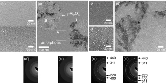
Figures 1(a)~(d) show bright field images (BFIs) of as-deposited and annealed Al2O3. No void
contrast can be detected in an as-deposited thin film although a fluctuation in the contrast is seen, as shown in Fig. 1(a). After annealing at 973 K for 3.6 ks (Fig. 1(b)), voids with a mean diameter of 1.9 nm appear, as is indicated by the bright contrast. As shown in the corresponding selected-area electron diffraction (SAED) patterns (a’) and (b’), the structure of the thin film remains amorphous
3
up to 973 K. At 1073 K, crystallized regions appear in the amorphous matrix, as can be seen in Fig. 1(c). The enlarged images corresponding to the amorphous (A) and crystallized (B) regions of Fig. 1(c), respectively, show that the voids in the crystallized region are larger than those in the amorphous region. The mean diameter of the nanovoids in the amorphous and crystallized regions was estimated to be 1.9 and 2.6 nm, respectively. The Debye-Scherrer rings can be consistently indexed as those of γ-Al2O3 (Fig. 1(c’)). The amorphous Al2O3 is fully crystallized into γ-Al2O3 at
1123 K and the mean diameter of nanovoids is 3.0 nm, as shown in Fig. 1(d). Our cross-sectional observation of a 200 nm-thick film revealed also that interior nanovoids were introduced inside the films after annealing at 973 K for 3.6 ks.
BFIs and the corresponding SAED patterns of a-WO3 thin film prepared by radio-frequency
sputtering at a substrate temperature of 100 K before and after annealing are shown in Fig. 2. Voids with diameters as small as 1.5 nm intrinsically appear as a result of the sputtering in the as-deposited film in Fig. 2(a). The microstructure of the as-deposited a-WO3 is consistent with the general
tendency that as-deposited films grown at very low temperature tend to be porous [14]. The growth of the existing voids is not clear at 573 K (Fig. 2(b)). At 623 K, however, crystalline regions appear in the amorphous phase, as shown in Fig. 2(c), as is the case with Al2O3. As seen from the magnified
images of the amorphous (A) and crystallized (B) regions in Fig. 2(c), a significantly high density of voids can be seen in the crystallized region, although the voids in the amorphous region did not grow as much as those in the films as-deposited and annealed at 573 K. It is obvious that the voids are much larger and are much more dense after the film is annealed at 673 K. The voids can be as large as 13 nm. The SAED patterns of Fig. 2(a’)-(d’) show that crystallization from amorphous to monoclinic WO3 starts at 623 K. We confirmed that the changes in the morphology and structure of
the thin films deposited at 273 K were similar to that at 100 K.
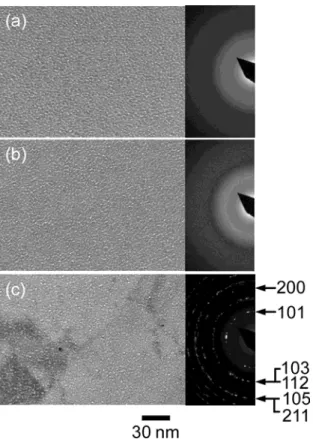
Figure 3 shows the BFIs of three different TiO2 thin films: (a) as-deposited, (b) annealed at
573 K, and (c) at 673 K. Their corresponding SAED patterns are indicated by (a’)~(c’). Amorphous structures are still apparent up to 573 K and then they are crystallized into anatase-type TiO2 at 673
K, as shown in Figs. 3(a’)-(c’). In an as-deposited a-TiO2, nanovoids as small as 1.5 nm are a
consequence of the deposition process, as was the case with a-WO3. The origin of nanovoids in
as-deposited films seems to be an intersection space of coalescence of islands [15]. In the case of TiO2, however, no change in the size or number of nanovoids is evident even after crystallization,
unlike Al2O3 and WO3.
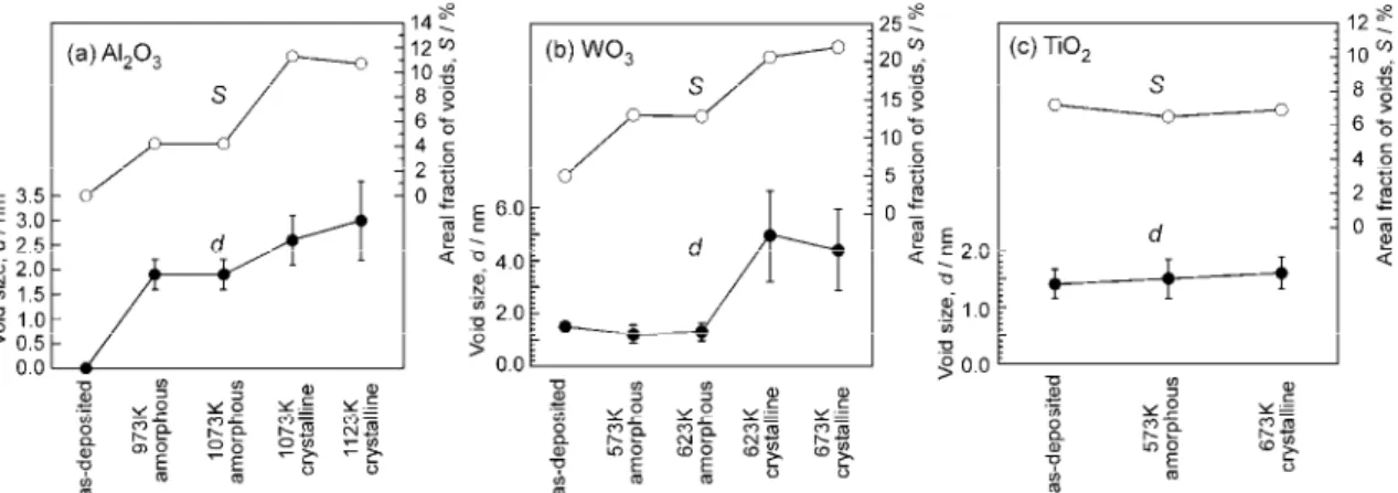
Figure 4 shows the changes in the average void diameter, d, and the areal fraction of the voids,
S, obtained by an image analysis of (a) Al2O3, (b) WO3, and (c) TiO2. The value of d is considered
equivalent to the diameter, assuming the voids are spherical and S is determined by dividing the sum of the occupied areas of voids by an area on a TEM image. Common characteristics were found in the void formation behavior in both Al2O3 and WO3: (i) S increases from as-deposited amorphous to
4
annealed amorphous, (ii) d and S are constant in the amorphous region (except as-deposited amorphous), and (iii) d and S increase with crystallization in the amorphous phase. The first characteristic suggests that the annealing of as-deposited amorphous Al2O3 and WO3 causes the new
formation of voids before crystallization. Although intrinsic voids are included in the as-deposited a-WO3 as mentioned earlier, the increase in S from the as-deposited amorphous stage to the
amorphous at 573 K clearly shows that, in addition to the existing voids, annealing results in the new generation of voids. Furthermore, the second and third characteristics indicate that crystallization accompanies the significant growth of voids. On the other hand, d and S for TiO2 remain constant
from the as-deposited state to crystalline phases, indicating that no voids are newly generated and the existing voids in an as-deposited film don’t grow with annealing.
It should be noted that the void generation and growth are observed after the annealing of a-Al2O3 and a-WO3 with 20-30% lower density than their crystalline phase. By contrast, no void
formation or growth is seen in a-TiO2, which has density much the same as its crystalline phase. The
results suggest that a large difference in density between the amorphous and crystalline phases seems to be an important factor for void formation. With regard to large differences in density between amorphous and crystalline phases, amorphous Ge and Si thin films prepared by vacuum evaporation are known to be 10~30% less dense than their crystalline phases [16-18]. A void network was observed in as-deposited Ge films in what were considered density-deficient regions below 1 nm in diameter [19]. A similar microstructure can be seen in our as-deposited a-Al2O3 (Fig. 1(a)); the
fluctuation of contrast in the range of 1 nm can be seen and the brighter regions seem to correspond to density-deficient regions with a significant number of free volume networks. Therefore, it would appear that significant number of free volume spaces, in other words, low density regions, tend to be common in the deposited amorphous state of Al2O3 and WO3 as is also the case with Ge and Si.
According to Moss and Graczyk [20], however, the voids in a-Ge tend to annihilate through annealing at high temperature. This is very different from what happens with a-Al2O3 and a-WO3,
however, since the voids in these oxides are generated as the annealing takes place. It is likely that the difference between oxides and Ge arises from the difference in structural change of these amorphous phases. It should be noted that in the case of amorphous oxides, at temperatures where long-range atomic diffusion occurs, existing free volumes are thought to condense to form nano-sized voids in the process of volume reduction along with crystallization. For the detailed discussion on the atomic level mechanism of void formation, temperature dependence on radial distribution function (RDF) of these amorphous oxides by analyzing electron diffraction patterns is under investigation and will be reported in the near future.
It is interesting to investigate how the composition deviation of as-deposited films from stoichiometry affects void formation behavior because both electron-beam evaporation and Ar sputtering techniques probably have an impact on the oxygen-deficiency of oxide thin films. The
5
EDS analysis on the composition of oxide films before and after annealing showed a qualitative tendency that the oxygen/metal ratio before annealing was either nearly equal to or even lower than that after annealing. A discussion on the quantitative composition should be avoided at this stage because of the inaccuracy of the composition of oxygen in the EDS analysis. However, under a stream of high-purity Ar with no supply of oxygen, a-Al2O3 and a-WO3 crystallized into γ-Al2O3 and
monoclinic WO3, respectively, and a high density of voids was formed, as was the case with
annealing in air. This result suggests that the deviation of composition of as-deposited films from stoichiometry is not so large and that void formation through the annealing of amorphous oxides is caused by the structural change from the amorphous to crystalline phases.
In conclusion, we have fabricated oxide nanoporous structures from amorphous Al2O3 and
WO3 through a simple heat-treatment process. We have demonstrated that a large difference in
density between amorphous and crystalline oxides can lead to the production of a high density of nanovoids. These porous nanostructures are expected to enable the application of Al2O3 and WO3 to
expand considerably; in the case of Al2O3, use in low-k materials [21] and humidity sensors [22] and
in the case of WO3, use in photocatalytic materials [23]. By itself, the ability to introduce of
nanovoids in materials amounts to a significant advance in technology since these nanovoids can act as gettering centers for metallic impurities in the design of devices [24-26]. Kooi et al. [27] and Hosson and Veen [26] have reported that sharply rectangular nano-sized voids can be obtained in helium-implanted and thermally annealed MgO(100) single crystals, suggesting that controlling the crystal growth of amorphous oxides can make it possible to produce faceted nanovoids. Therefore, further researches on how to control not only the size and density of nanovoids but also their size and density and to extend the technique to fabrication of other metal-oxides are required.
The authors would like to thank emeritus Prof. H. Mori and Mr. E. Taguchi of Research Center for Ultra-High Voltage Electron Microscopy, Osaka University, for carrying out the TEM observations. This work was supported by Grant-in-Aid for Young Scientists (B) (No. 21760556) and also by Priority Assistance for the Formation of World Wide Renowned Centers of Research - The Global COE Program (Project: Center of Excellence for Advanced Structural and Functional Materials Design), from the Ministry of Education, Culture, Sports, Science and Technology, Japan.
References
[1] C.T. Kresge, M.E. Leonowicz, W.J. Roth, J.C. Vartuli, J.S. Beck, Nature 359 (1992) 710. [2] S.A. Johnson, P.J. Ollivier, T.E. Mallouk, Science 283 (1999) 963.
[3] P. Yang, D. Zhao, D.I. Margolese, B.F. Chmelka, G.D. Stucky, Nature 396 (1998) 152.
[4] Y. Yin, R.M. Rioux, C.K. Erdonmez, S. Hughes, G.A. Somorjai, A.P. Alivisatos, Science 304 (2004)711.
6
[5] H.J. Fan, M. Knez, R. Scholz, K. Nielsch, E. Pippel, D. Hesse, M. Zacharias, U. Gösele, Nat Mater 5 (2006) 627.
[6] K. Yoshimi, M. Tsunekane, R. Nakamura, A. Yamauchi, S. Hanada, Appl. Phys. Lett. 89 (2006) 073110.
[7] D. Weaire, M. F. Ashby, J. Logan, M. J. Weins, Acta Metall. 19 (1971) 779.
[8] C. Landron, L. Hennet, T.E. Jenkins, G.N. Greaves, J.P. Coutures, A.K. Soper, Phys. Rev. Lett. 86 (2001) 4839.
[9] M. S. Mattsson, Phys. Rev. B 58 (1998) 11015. [10] Y. Kimura, C. Kaito, J. Crys. Growth 250 (2003) 450.
[11] L.J. Alvarez, L.E. Leon, J.F. Sanz, M.J. Capitan, J.A. Odriozola, Phys. Rev. B 50 (1994) 2561. [12] L.J. Alvarez, L.E. Leon, J.F. Sanz, M.J. Capitan, J. Odriozola, Surf. Sci. 322 (1995) 185. [13] T. Nakamura, T. Ichitsubo, E. Matsubara, A. Muramatsu, N. Sato, H. Takahashi, Acta Mater. 53 (2005) 323.
[14] R.W. Smith, D.J. Srolovitz, J. Appl. Phys. 79 (1996) 1448. [15] J.R. Lloyd, S. Nakahara, J. Vac. Sci. Tech. 14 (1977) 655. [16] S.C. Moss, J.F. Graczyk, Phys. Rev. Lett. 23 (1969) 1167. [17] A.H. Clark, Phys. Rev. 154 (1967) 750.
[18] T.M. Donovan, W.E. Spicer, J.M. Bennett, Phys. Rev. Lett. 22 (1969) 1058. [19] T.M. Donovan, K.Heinemann, Phys. Rev. Lett. 27 (1971) 1794.
[20] S.C. Moss, J.F. Graczyk, Phys. Rev. Lett. 23 (1969) 1167.
[21] P.A.R.D. Jayathilaka, M.A.K.L. Dissanayake, I. Albinsson, B.E. Mellander, Electrochim. Acta 47 (2002) 3257.
[22] J.J. Steele, M.T. Taschuk, M.J. Brett, Sensors Journal, IEEE 8 (2008) 1422.
[23] C. Santato, M. Odziemkowski, M. Ulmann, J. Augustynski, J. Am. Chem. Soc. 123 (2001) 10639.
[24] C.C. Griffioen, J.H. Evans, P.C. De Jong, A. van Veen, Nucl. Instrum. Methods B 27 (1987) 417.
[25] R. D. Miller, Science 286 (1999) 421.
[26] J.Th.M.De Hosson, A. van Veen, Nanoprecipitates and nanocavities in functional materials, in: H.S. Nalwa (Ed), Encyclopedia of Nanoscience and Nanotechnology (Vol. 7), American Scientific Publishers, Valencia, 2004, pp.297-349.
[27] B.J. Kooi, A. van Veen, J.T.M.De Hosson, H. Schut, A.V. Fedorov, F. Labohm, Appl. Phys. Lett. 76 (2000) 1110.
7
FIG. 1. BFIs of amorphous Al2O3 before (a) and after annealing for 3.6 ks at (b) 973, (c) 1073, and
(d) 1123 K. Magnified images (A) and (B) correspond to the amorphous and crystalline regions enclosed by a square in (c), respectively. (a’)-(d’) show the corresponding SAED patterns.
8
FIG. 2. BFIs of amorphous WO3 before (a) and after annealing for 3.6 ks at (b) 573, (c) 623, and (d)
673 K. Magnified images (A) and (B) correspond to the amorphous and crystalline regions enclosed by a square in (c), respectively. (a’)-(d’) show the corresponding SAED patterns.
9
FIG. 3. BFIs of amorphous TiO2 before (a) and after annealing for 3.6 ks at (b) 573, and (c) 673 K.
10
FIG. 4. Changes in the average void size, d, and areal fraction of voids, S, for (a) Al2O3, (b) WO3,