INVITED PAPER
Special Section on Electronic DisplaysLow-Power Driving Technique for 1-Pixel Display Using an External Capacitor
Hiroyuki MANABE†a),Member, Munekazu DATE††, Hideaki TAKADA††,Nonmembers, andHiroshi INAMURA†,Member
SUMMARY Liquid crystal displays (LCDs) are suitable as elements underlying wearable and ubiquitous computing thanks to their low power consumption. A technique that uses less power to drive 1-pixel LCDs is proposed. It harvests the charges on the LCD and stores them in an exter- nal capacitor for reuse when the polarity changes. A simulation shows that the charge reduction depends on the ratio of the capacitance of the external capacitor to that of the LCD and can reach 50%. An experiment on a proto- type demonstrates an almost 30% reduction with large 1-pixel LCDs. With a small 10×10 mm2LCD, the overhead of the micro-controller matches the reduction so no improvement could be measured. Though the tech- nique requires longer time for polarity reversal, we confirm that it does not significantly degrade visual quality.
key words: LCD, PDLC, 1-pixel, low power, capacitor
1. Introduction
Liquid crystal displays (LCDs), which control light electri- cally, are essential elements in everyday life. Multiple-pixel displays yield monitors or TVs while single-pixel displays provide shutters or light control glasses. Additionally, var- ious ubiquitous and wearable devices have been developed and they are becoming widespread in our everyday environ- ment. They will allow users to interact with daily objects and to access huge amounts of information anytime, any- where, via wearable, always-on devices. Since the power consumption of LCDs is generally quite small, they suit ubiquitous or wearable devices. However, even lower power consumption is a critical requirement in building practical ubiquitous or wearable devices, because it extends the bat- tery life and makes the devices smaller.
Examples of LCD-based devices include the active tags that we have developed[1]. The tag consists of a 1-pixel display with PDLC (polymer dispersed liquid crystal), a retroreflector, a micro-controller and a power source, see Fig.1. The tag sends its ID by switching the PDLCD (PDLC display) to modulate the light emitted from the tag reader.
An IR-based depth sensing camera emitting continuous IR can be used as the tag reader. Since the transmittance of the PDLCD is high and the retroreflector reflects light strongly, the tag can be decoded even if its physical size occupies less
Manuscript received February 27, 2015.
Manuscript revised June 2, 2015.
†The authors are with Research Labs, NTT DOCOMO, Yokosuka-shi, 239–8536 Japan.
††The authors are with NTT Media Intelligence Labs, NTT Cor- poration, Yokosuka-shi, 239–0847 Japan.
a) E-mail: [email protected] DOI: 10.1587/transele.E98.C.1015
Fig. 1 Active tags with 1-pixel PDLCDs[1]; one of the target applica- tions of this technique. The tag consists of a PDLCD, a retroreflector, a micro-controller and a power source and sends its ID by switching the PDLCD. Three kinds of power sources were implemented; the left has a lithium coin battery, the middle an amorphous photovoltaic module (PV), the right a single crystal PV. Reduction in power consumption allows fur- ther miniaturization.
than one pixel on the image captured by the camera. Thanks to this advantage and its low power operation, the tag can be miniaturized, which is an important factor in making such tags useful in everyday life. Further miniaturization is de- sired to improve its acceptance and reducing the power con- sumption, especially that used to drive the LCD, is the key to achieve it.
Assuming the target to be 1-pixel devices with binary operation and square wave driving voltage such as used in our active tags, the proposed technique with its external ca- pacitor can reduce the current and its time integral, charge, needed for polarity reversal. A simulation that treats the LCD as a capacitor shows that the technique can reduce the current and experiments on three PDLCDs of different sizes confirm its effectiveness and limitation. The negative aspect of the technique, more time is needed for polarity reversal, is also evaluated. While a preliminary version of this work has already been reported[2], this paper describes further experiments and deeper analyses.
2. Related Work
Many small devices which interact with the user have multi- pixel or matrix LCDs, for example, smartphones and smart watches. Such LCDs can provide a lot of information to the user with little power consumption. Reducing power consumption without degrading display quality is essential and several techniques have been already proposed for ac- tive matrix LCDs. Their basic idea is charge sharing to address the issue that dot inversion provides the best dis- play quality but consumes more power than either frame or line inversion. For example, simply shortening neigh- Copyright c⃝2015 The Institute of Electronics, Information and Communication Engineers
shared among the pixels and, in some cases, external capac- itors. For plasma display panels (PDP), one technique uses the resonance between inductors and the PDP to improve overall power efficiency[9]. Reducing power consumption without hardware modification can be achieved by software- only techniques such as variable dot clock, variable frame refresh, liquid crystal orientation shift, and backlight lumi- nance dimming[10],[11].
Unlike multi-pixel LCDs, 1-pixel LCDs, the target of the proposed technique, are used in far more applications than just information display. One of them, the smart glasses, takes three different approaches: electrochromic glass, suspended particle glass, and LC glass[12]. Ap- plication examples of large smart glasses include architec- tural glass, automobile, and aircraft[13]. A major disad- vantage of the smart glass, the need for a voltage source, can be resolved by the integration of photovoltaic (PV) de- vices[12],[13], which means lower power consumption is desirable. PDLCD[14], one type of smart glass, is often used to realize electrically controlled privacy glass thanks to its scattering property[15]. PDLCDs generally scatter light when they are OFF and transparent when ON, and a reverse mode PDLCD works as expected[16]. Such optical characteristics offer various applications. Squama, which consists of PDLCD tiles and forms programmable physical windows or walls, dynamically controls the visibility of its tiles according to the user’s needs[17]. Polymer stabilized cholesteric textured liquid crystals, like PDLCD, are used as dynamic screens to enhance interactive surface technol- ogy[18]. While regular LCDs require polarizers and total transmittance becomes less than 50%, PDLCDs do not and transmittance can exceed 80%. There are various PDLC applications that focus on its high efficiency. In the ac- tive tag[1]mentioned before, using a PDLCD can extend the readable range. Eye glasses with PDLCDs to prompt the user to blink offer high transmittance and do not disturb daily activity[19]. The benefits of the PDLC are not limited to 1-pixel displays, multi-pixel displays are also possible.
For example, the segmented PLNC (polymer network liquid crystal) display consumes ultra low power[20], and a direct- viewing display with PDLCs can provide high optical effi- ciency[21]. Normal LCDs are also used as 1-pixel displays rather than PDLCD, but mainly as a shutter. Stereoscopic systems uses LC shutters[22]. The characteristics of LCs including power consumption and response time were inves-
the conventional techniques can not be directly applied to 1-pixel displays since there are several differences between active matrix and 1-pixel displays. For example, the inver- sion method can be used for active matrix displays but not for 1-pixel displays; the former has one capacitor for each pixel while the latter does not.
3. Proposed Technique
The proposed technique is based on the charge sharing tech- niques that have been examined for active matrix LCDs[3]–
[8], but it is specifically tuned for 1-pixel displays. The dif- ferences include that the LCD itself is used as a capacitor, no inversion method is applied, only two voltages are used to simplify the operation, and polarity reversal can take longer.
The technique does not share the charge within pixels but uses an external capacitor to harvest and reuse the charge.
3.1 Operation Flow
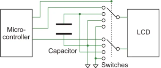
The simplest driving circuit for a 1-pixel display has a micro-controller with two pins; we need only to output HIGH and LOW via the pins and invert the pin state for polarity reversal. A 1-pixel LCD resembles, in some ways, a capacitor, as large current flows at every polarity reversal while little current flows during stable state. The proposed technique requires an external capacitor and analog switches to harvest and reuse the charge. A possible circuit, shown in Fig.2, uses a dual 4:1 multiplexer as analog switches; the operation flow for the circuit is shown in Fig.3.
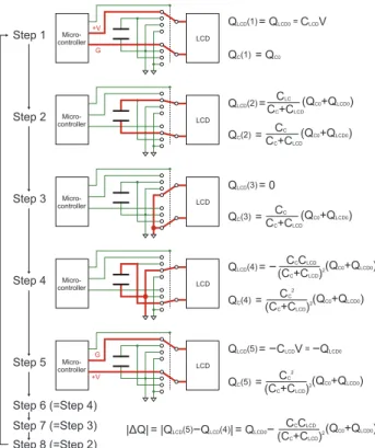
The simplest operation repeats Steps 1 and 5, which is defined as regular operation (i). If one more step is added to short the LCD during the polarity reversal, which in- volves Steps 1, 3, 5, and 7, the charge the micro-controller
Fig. 2 An example of a circuit to implement the proposed technique. The circuit for the proposal includes an external capacitor, a micro-controller, and analog switches (a dual 4:1 multiplexer).
Fig. 3 Operation flow of the technique for one cycle (two polarity rever- sals). While regular operation has two steps (Steps 1 and 5) or four steps (Steps 1, 3, 5 and 7), the proposed technique has eight steps. |∆Q|is the charge the micro-controller has to supply to change the polarity of the LCD;
in regular operation it is 2QLC0or QLC0. It theoretically becomes 0.5QLC0
when CCis much larger than CLCDand the cycle count goes up enough.
The reduction can reach 25% or 50% in such situations.
has to supply becomes smaller than the regular operation (i), which corresponds to the technique in[3] for the ac- tive matrix LCD and defined as regular operation (ii). These regular operations can be performed simply by a micro- controller with two pins without a capacitor or switches.
The proposed technique has eight steps to harvest and reuse the charge. Since the capacitor charges the LCD (Steps 4 and 8) before the micro-controller does (Steps 1 and 5), the micro-controller can reduce the current sent to the LCD. The charge on the LCD moves to the capacitor (Steps 2 and 6) before the LCD is shortened (Steps 3 and 7).
Assuming that the LCD is an ideal capacitor with ca- pacitance of CLCDand the external capacitor has capacitance of CC, the charges on the LCD and capacitor in these steps, starting with QLCD0 and QC0 in Step 1, are calculated as shown in Fig.3. Since Steps 5 to 8 are merely reversed op- erations, it is enough to focus on one half of the operations.
When|∆Q|is defined as the charge the micro-controller has to supply for a polarity reversal,|∆Q|is equal to 2QLCD0 in regular operation (i) and QLCD0 in (ii), and it is reduced as described in Fig.3when the proposed technique is applied.
|∆Q|depends on the initial charge of capacitor QC0 at each cycle, which changes as the operation proceeds. Assuming the operation becomes stable (saturated) without oscillation, QC(1) and QC(5) would have the same value. In this case,
|∆Q|is given as follows,
Fig. 4 Simulation result. The charge supplied by the micro-controller under saturated situation and the cycle count to reach such a situation de- pends on the capacitance of the external capacitor. For example, largekcan achieve high reduction but many cycles are needed before such reduction can be realized.
|∆Q|= CC+CLCD
2CC+CLCDQLCD0 (1)
If CC is much larger than CLCD, |∆Q| becomes 0.5QLCD0. That is, the technique reduces the charge to be supplied by up to 25% and 50% compared with regular operation types (i) and (ii).
3.2 Simulation
Though |∆Q| under the saturated situation is calculated above, the exact status of operation is unclear. Before build- ing and evaluating a prototype, we conducted a simulation on a PC to grasp the performance of the technique. In this simulation, CC is given as kCLCD using coefficient k and the average of two|∆Q|/QLCD0values which correspond to
|QLCD(5)−QLCD(4)|and|QLCD(8)−QLCD(1)|, is used as an index for one cycle. Since in the initial state before Step 1, both the LCD and capacitor have zero charge, half of the in- dex in the first cycle is 1. Note that the value directly reflects the supplied charge ratio compared with regular operation (ii).
Figure4shows the simulation results. The vertical axis plots the ratio of supplied charge. The effectiveness depends on coefficientk; smallkhas little impact on charge reduction while large values are effective, as was implied above. It re- veals that the number of cycles to convergence also depends onk.
Figure 5 shows another simulation result: the rela- tionship between the supplied charge ratio under the satu- rated situation and the cycle count needed. The thin black line plots the limit value calculated from (1) and the thick line corresponds to its 99% level, an example used in cal- culating the required cycle count. The blue line shows the cycle count needed to reach the 99% level. The cycle count needed is linear tok, which implies that mediumkis most effective in actual systems, because the improvement matches that possible with largekand the maximum current reduction is quickly achieved.
Fig. 5 Simulation result of the charge ratio under saturated situation (black solid line refers to left axis) and cycle count needed to reach its 99%
level (blue line refers to right axis). Cycle count is linear to the capacitance ratiok, and the improvement saturates whenkis over several decades even if many cycle counts are used.
Note that the simulation can be applied in several driv- ing patterns. When the LCD continuously keeps its ON state with periodic polarity reversals for smart glass appli- cation, the micro-controller sleeps in Steps 1 and 5 which have longer duration, while the other durations are shorter.
When the LCD state changes rhythmically as for the active tag and eye glasses[19], a longer OFF state is easily pro- vided by holding Steps 3 and 7 with the micro-controller in the sleep state.
4. Evaluation
The simulation made several assumptions; the LCD is just a capacitor, the micro-controller works quite quickly with zero power consumption, and no leak currents and no resis- tance exist. Actual devices, however, render these assump- tions invalid. Since it is important to confirm the technique with an actual prototype, experiments were conducted to confirm the technique. Three PDLCDs and the two devel- oped circuits were tested to confirm positive and negative aspects of the technique.
4.1 Experiment Setup
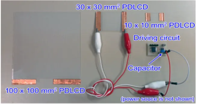
Figure6 shows the experimental setup including tested 1- pixel PDLCDs and the prototype circuit. The PDLCDs, which were developed for low voltage operation, 3 V (6 V in peak-to-peak), by Seiko Electric[24]were used. Three PDLCDs of different sizes were tested to measure the to- tal performance, which depends in part on PDLCD size due to the offset of the micro-controller. They are labeled as 100 × 100 mm2, 30 × 30 mm2, and 10 × 10 mm2 PDL- CDs, and their effective area was about 98 × 98 mm2, 28 × 28 mm2, and 10 × 10 mm2, respectively. The capac- itance of the PDLCDs measured by an LCZ meter were 70 nF , 7 nF, and 1 nF at 50 Hz, respectively. Note that these values are typical and differ among samples even of the same size.
circuit. The capacitor is easily replaced. This figure does not show the voltage source or the picoammeter.
The circuit consists of a PIC micro-controller, 16LF1847 working at 31 kHz, a dual 4:1 multiplexer, MAX4639, and two small capacitors (0.1µF) as bypasses for the two elements. The micro-controller is activated ev- ery 18 ms (this sleep time corresponds to Steps 1 and 5) to control the flows; overall, it takes about 36ms for one cy- cle, from Steps 1 to 8. The PDLCDs were kept in the ON state in this driving pattern. The tested capacitors had val- ues of 0.22 nF, 2.2 nF, 0.022µF, 0.22µF, 2.2µF, 22µF, and 220µF, the first six were ceramic and the last one was an electrolytic capacitor. The external voltage source provided 3 V to the circuit though a resistor, 100Ω(except 510Ωfor regular operation (i) for 30 × 30 mm2PDLCD) to limit the current so that the current did not exceed the dynamic range of the picoammeter. The current flows were measured 5 s, 30 s, 60 s, 120 s, 180 s, 240 s, and 300 s after the initial activation.
4.2 Measured Current
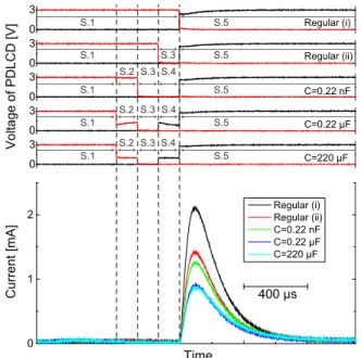
Figure7shows the values with the 100 × 100 mm2PDLCD under regular operation (i) and (ii) and the proposed tech- nique with three capacitors at 180s after initiation. The up- per graphs show the voltages at the ends of the PDLCD and the lowest shows the current. While PDLCD voltages were simply changed under regular operation (i) corresponding to Steps 1 and 5, (ii) for Steps 1, 3, and 5, more complicated voltage traces were observed with the proposed technique from Steps 1 to 5. Large current flowed at the beginning of Step 5 in all operations (lower graph), which corresponds to the current needed to charge the LCD; its time integration corresponds to |∆Q|. This large current caused a voltage drop at the current limiting resistor, which resulted in the voltage at the beginning of Step 5 being gradually increased to 3 V. The current then slowly decreased, which might be due to the bypass capacitors. Compared to regular opera- tion, the proposed technique successfully reduced the cur- rent in Step 5. The averaged current over 2 ms, which corre- sponds to the time range of the figure, was 0.30 mA and 0.21 mA for regular operation (i) and (ii) and 0.20 mA (C=0.22 nF), 0.15 mA (C=0.22µF), and 0.16 mA (C=220µF) for the proposed technique.
Fig. 7 Measured current with 100×100 mm2 PDLCD. The upper graphs show the voltage at the two ends of the PDLCD. While regular op- erations (i) and (ii) yielded simple traces, that with the proposed technique was complex. The lowest graph shows the current. Large current was re- quired at the beginning of Step 5, shown by “S.5” in the figure, and the proposed technique successfully reduced this current.
Figure 8 shows the results for the 30 × 30 mm2 PDLCD at 180 s after initiation. Though PDLCD voltages seem the same as those for the 100 × 100 mm2PDLCD, the current trace is different. Note that the shape of the current trace for regular operation (i) differs due to use of a larger resistance to limit the current. One similarity is the success- ful reduction in the large current peak of Step 5. However, a small peak was observed before Step 5 or 3 in regular opera- tion (i) or (ii) and Step 2 in the technique, which corresponds to the current needed to wake up the micro-controller. The small peaks created by the regular and proposed technique seem almost the same, but the duration between the peaks during which some current flowed, differs due to the op- eration steps (compare regular (ii) to the proposal). This additional current and the long operating duration decrease the efficiency of the proposed technique. The averaged cur- rent (2 ms duration) was 29µA and 19µA for regular oper- ation (i) and (ii) and 13µA for the proposed technique with 0.22µF capacitor.
The current history of the 10 × 10 mm2 PDLCD at 180 s after initiation is shown in Fig.9. The current trace recorded without any PDLCD is also shown; it represents the operations of the micro-controller and the multiplexer.
The current for the micro-controller’s operation is clearly measured. It is observed that the peak at the beginning of Step 5 is reduced with the technique same as for other PDL- CDs. However, its reduction is small due to the small dimen- sions of the LCD, and is comparable to the current addition- ally consumed by micro-controller operation. The averaged current (2 ms duration) was 8.0µAand 6.4µA for regular operation (i) and (ii) and 6.4µAfor the proposed technique
Fig. 8 Measured current with 30×30 mm2 PDLCD. The proposed technique reduced the current in Step 5, however the power consumed by the micro-controller is not negligible. Note that in regular operation (i), the peak current seems lower and keeps high for longer since a large resistance was used to limit the current.
Fig. 9 Measured current with 10×10 mm2PDLCD. The current with no PDLCD is also shown in the graph. The technique reduced the current at the beginning of Step 5, the same as with the other PDLCDs. However, the power consumed by the micro-controller, needed for wakeup and switching operation, became comparable to that consumed by the polarity change of the LCD. While wakeup current was needed for all techniques, the longer operation time needed for this PDLCD increased the current consumption.
The overall benefit corresponds to the difference between them.
with 0.22µFcapacitor.
4.3 Supplied Charge vs. Capacitance
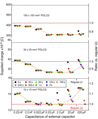
Figure 10shows the relationship between supplied charge and the capacitance of the external capacitor. The charge was calculated as the time integration of the current over 2 ms periods. The values at various times after initiation are plotted and those for 180 s are connected with a solid line. For the 10 × 10 mm2 PDLCD, the charges at 1- and 3-hours after initiation are plotted. The ratio compared to regular operation (ii) is indicated on the right axis.
Fig. 10 Supplied charge vs. capacitance of the external capacitor. The charge was measured over time after initiation. It decreased as capacitance increased when the capacitance is smaller, which corresponds to quick sat- uration. When larger capacitance was applied, many cycles were needed before the charge was reduced, as is clearly found with the 10×10 mm2 PDLCD. Compared to regular operation (ii), the reduction reached almost 30% with 100×100 mm2and 30×30 mm2PDLCDs, however no im- provement was measured with the 10×10 mm2PDLCD because the over- head of the micro-controller offsets the proposal’s reduction in LCD cur- rent.
The reduction in charge depends on the capacitance and the size of the PDLCD. For example, the charge with the 100 × 100 mm2 PDLCD decreases as the capacitance increases when the capacitance is small but seems saturated when the capacitance is large. This is also found with the 30 × 30 mm2 and 10 × 10 mm2 PDLCDs. However the reduction with a specific capacitor changes according time, especially with large capacitors. Comparing 2.2µF, 22µF, and 220µF in the 10 × 10 mm2PDLCD, it is clearly seen that longer times are required with larger capacitors. This result matches the simulation result that indicates the cycle count needed is linear to the capacitance ratiok.
Considering the efficiency against regular operation (ii), it was successfully improved with the 100 × 100 mm2 and 30 × 30 mm2 PDLCDs. Almost 30% reduction was achieved (maximum reduction was measured with 0.22µF and 100 × 100 mm2 PDLCD at 30 s as 27.7%, 22µF and 30x30mm PDLCD at 180 s as 29.8%). Since the micro-controller’s current was relatively small for the 100 × 100 mm2 PDCLD, a larger reduction was expected than that achieved with the 30 × 30 mm2 device. One of the possible reasons is the large leak current of the tested PDLCD. There is no improvement with the 10 × 10 mm2 PDLCD because the overhead of the micro-controller’s cur- rent cancels the effect. The charge needed to drive just the
action times; about 20 ms to change to transparent and 170 ms to scattering (these values correspond to a transparency change from 10% to 90%). While one of the drawbacks of the technique is that longer time (about 400µs) is required to realize polarity reversal as it takes multiple steps, it has negligible impact on the active tag’s operation.
The standard PDLCD usage is smart glass in which the PDLCD tends to keep its state, ON or OFF, for a long time and human-perceptible performance is important, unlike the tag. Lowering the driving frequency is a major approach to reducing the power consumption[10],[11],[20]and com- bining with it the proposed technique would offer higher ef- ficiency. In such LCD-based applications with infrequent polarity reversal, longer time for polarity reversal, may im- pact the LCD service quality by creating flicker. Note that when ON state is kept for 400 ms in the active tag, one polar- ity reversal during the period causes human-visible flicker, however, the tag’s ID is successfully decoded. This flicker test is intended for human-visible evaluation assuming smart glass usage.
We determined the conditions under which flicker was perceived by eight subjects (all males from 25-38 years old) using the 100 × 100 mm2PDLCD with the proposed tech- nique and regular driving (ii) in a regular office environment, where LED fluorescent tubes driven at 106 kHz were used as ceiling lights. The driving circuit implemented for this experiment differed from that of the previous experiment.
The voltage applied to the PDLCD was 3 V, the same as in the previous experiment, which was sufficient to saturate its optical characteristics. This experiment includes two tests:
flicker threshold and determining whether the difference is perceptible.
The flicker threshold test proceeded as follows. The sleep time for Steps 1 or 5 were changed sequentially every 6.3 s from 15, 19, 23, 27, 31, 35, 39, to 43 ms. Since other steps took shorter time durations shown as Figs.7,8, and9, the PDLCD always held the ON state, with flicker in some cases. Before starting the experiment, the subject was asked to carefully watch the PDLCD to detect the flicker created by its operation. In this training period of a few minutes, the subject could change the placement of the PDLCD to maximize flicker detection. The placement was fixed be- fore commencing the experiment. The sleep time at which the subjects first perceived the flicker was recorded. This test was repeated 5 times for each technique. Some subjects
picked the same specific sleep time, e.g. 31 ms for all 5 tri- als, but the others picked different times in every trial, e.g.
31 ms for 2 trials and 35 ms for 3 trials. The thresholds, the median for the five values, depended on the subject from 23 to 35 ms; five subjects had the same values for both driving techniques, two had larger value with the regular operation, and one showed the opposite.
After the flicker threshold test, the second test started.
This test examined whether the subject could perceive the difference between the two driving techniques with the same sleep time. The controller switched between the regular driving (ii) and the proposed technique every 2.1 s with the same sleep time, and the subject was asked whether there was any differences between the two. Note that no differ- ence does not mean no flicker in this test. The sleep time was varied manually after the subject answered. Five subjects reported that some difference could be seen after careful watching when sleep times equaled or exceeded the flicker threshold. Even the subjects whose flicker threshold for the proposal were different from that for the regular one, could not detect the difference when the sleep time was set shorter than the threshold for regular driving. Since the driving fre- quency is generally selected so as to avoid flicker, shorter sleep times than the threshold in this test, the test confirms that the proposal does not degrade LCD visual quality from the viewpoint of human visual capability. Considering the standard usage of PDLCDs, the visual comparison provides useful data for practical use. These results confirm that the sleep time can be set to 23 ms (or less) with the tested PDLCDs which together with lowering driving frequencies, will further lower the power consumption. For example, 3.9×10⁻⁵J (0.15 mA×3 V×2 ms×1000 ms/23 ms) was needed for polarity reversals per second (C=0.22µF) when the sleep time was 23 ms, while 6.0 × 10⁻⁵ J when it was 15 ms.
5. Conclusion
A technique that improves the efficiency with which a 1- pixel LCD can be driven was proposed. It harvests the charge on the LCD and stores it in an external capacitor for reuse when the polarity of the driving voltage changes. Its performance was simulated and measured by testing a pro- totype. The simulation showed that charge reductions of up to 50% compared with regular operation (ii), were possible and that the degree of reduction and the time taken to reach current saturation depend on the ratio of the capacitance of the capacitor to that of the LCD. The improvement was con- firmed in the experiment and the overall reduction in sup- plied charge was almost 30% when the micro-controller’s power consumption was relatively small. Unfortunately the experiment showed that the overhead of the micro-controller (its power consumption) is significant for small LCDs. An additional experiment confirmed that the increase in time taken by the proposed technique to effect polarity reversal had little impact on the degree of flicker perceived.
When the active tag[1]uses a 10 × 10 mm2PDLCD
as one of the target applications, the proposed technique (in its current prototype) is unable to contribute to tag miniatur- ization. Further improvements are needed, for example, us- ing multiple capacitors for more effective power reduction and a low power micro-controller. Though the technique currently does not suit tiny tags, there are several possible applications such as, light control glasses[19]in which the proposed technique would be effective.
References
[1] H. Manabe, W. Yamada, and H. Inamura, “Tag system with low- powered tag and depth sensing camera,” Proc. UIST ’14, pp.373–
382, 2014.
[2] H. Manabe, M. Date, H. Takada, and H. Inamura, “Low-power liq- uid crystal driving technique based on capacitors for 1-pixel dis- plays,” Proc. IDW ’14, pp.1343–1346, 2014.
[3] S.T. Kim, B.D. Choi, and O.K. Kwon, “A novel method of charge- recycling TFT-LCD source driver for low-power consumption,”
Proc. IDW ’97, pp.155–158, 1997.
[4] A. Erhart and D. McCartney, “Charge-conservation implementation in an ultra-low-power AMLCD column driver utilizing pixel inver- sion,” SID ’97 Digest of Technical Papers, no.1, pp.23–26, 1997.
[5] Y.C. Sung, B.D. Choi, and O.K. Kwon, “A low-power data driver for TFT-LCDs,” SID ’00 Digest of Technical Papers, vol.31, no.1, pp.142–145, 2000.
[6] S.S. Yang, P.L. Guo, T.Y. Chang, and J.H. Hong, “A multi-phase charge-sharing technique without external capacitor for low-power TFT-LCD column drivers,” Proc. ISCAS ’03, pp.V–365–V–368, 2003.
[7] J.-S. Kim, D.-K. Jeong, and G. Kim, “A multi-level multi-phase charge-recycling method for low-power AMLCD column drivers,”
IEEE J. Solid-State Circuits, vol.35, no.1, pp.74–84, 2000.
[8] B.D. Choi and O.K. Kwon, “Stepwise data driving method and cir- cuits for low-power TFT-LCDs,” IEEE Trans. Consum. Electron., vol.46, no.4, pp.1155–1160, 2000.
[9] H.B. Hsu, C.L. Chen, S.Y. Lin, and K.M. Lee, “Regenerative power electronics driver for plasma display panel in sustain-mode opera- tion,” IEEE Trans. Ind. Electron., vol.47, no.5, pp.1118–1125, 2000.
[10] F. Gatti, A. Acquaviva, L. Benini, and B. Ricco’, “Low power con- trol techniques for TFT LCD displays,” Proc. CASES ’02, pp.218–
224, 2002.
[11] I. Choi, H. Shim, and N. Chang, “Low-power color TFT LCD dis- play for hand-held embedded systems,” Proc. ISLPED ’02, pp.112–
117, 2002.
[12] K.V. Wong and R. Chan, “Smart glass and its potential in energy savings,” J. Energy Resources Technology, vol.136, no.1, p.012002, 2014.
[13] C. Lampert, “Large-area smart glass and integrated photovoltaics,”
Solar Energy Materials and Solar Cells, vol.76, no.4, pp.489 – 499, 2003.
[14] P.S. Drzaic, “Polymer dispersed nematic liquid crystal for large area displays and light valves,” J. Applied Physics, vol.60, no.6, pp.2142–2148, 1986.
[15] C.M. Lampert, “The world of large-area glazing and displays,” Proc.
SPIE, pp.2–11, 1999.
[16] M. MacChione, D. Cupelli, G.D. Filpo, F.P. Nicoletta, and G. Chidichimo, “Morphology and electro-optical properties of re- verse mode polymer dispersed liquid crystals,” Liquid Crystals, vol.27, no.10, pp.1337–1341, 2000.
[17] J. Rekimoto, “Squama: modular visibility control of walls and windows for programmable physical architectures,” Proc. AVI ’12, pp.168–171, 2012.
[18] S. Izadi, S. Hodges, S. Taylor, D. Rosenfeld, N. Villar, A. Butler, and J. Westhues, “Going beyond the display: a surface technology with
technologies,” Displays, vol.17, no.2, pp.100 – 110, 1997.
[23] P. Xu, X. Li, V.G. Chigrinov, and S.A. Studentsov, “Fast and high- contrast liquid-crystal shutters with low power consumption based on an optical-mode-interference cell,” Appl. Opt., vol.45, no.17, pp.4020–4025, 2006.
[24] Seiko electric, “SILF (in Japanese).” http://www.seiko-denki.co.jp/ product/component/component05.php (accessed in Jan. 2015).
Hiroyuki Manabe was born in 1976. He received the B.E., M.E., and Ph.D. degree from Tokyo Institute of Technology in 1999, 2001, and 2015, respectively. He joined NTT DO- COMO in 2001 and have worked on HCI field.
His interests include wearable computing, ubiq- uitous computing, input devices, and biological signal processing. He is a member of IPSJ and ACM.
Munekazu Date received the B.S. de- gree in physics from Gakushuin University, To- kyo, Japan in 1990, an M.E. degree in applied electronics from Tokyo Institute of Technology, Yokohama, Japan, in 1992, and the Ph.D. de- gree in Chemistry from Tokyo University of Sci- ence, in 2003. He has been with Nippon Tele- graph and Telephone (NTT) Corporation, To- kyo, Japan since 1992. There, he has been en- gaged in research on holographic optical devices using polymer/LC composites and 3D displays.
He joined NTT COMWARE Corporation, Chiba, Japan in 2010 and re- joined NTT Corporation in 2012. Dr. Date is a member of the Society for Information Display, the Institute of Electrical and Electronics Engineers, the Japanese Liquid Crystal Society, the Institute of Electrical Engineers of Japan, Holographic Display Artists and Engineers Club and Consortium of 3-DBusiness Promotion.
engaged in the research of 3D visual perception and 3D display technol- ogy. He has received the Best Paper Award from the 3-D image conference in 2001, the Young Researcher’s Award from the Virtual Reality Society of Japan (VRSJ) in 2002, the Achievement Award from the Institute of Electronics, Information and Communication Engineers (IEICE) in 2003, and Commendation by the Minister of Education, Culture, Sports, Science, and Technology in 2006. He is a member of the Institute of Electrical and Electronics Engineers (IEEE), and the Institute of Image Information and Television Engineers (ITE).
Hiroshi Inamura joined NTT DOCOMO, Inc. in 1998. His research interests include sys- tem research on mobile device and distributed system. Before DOCOMO, he was a research engineer in NTT labs since 1990. From 1994 to 1995, he was a visited researcher in the De- partment of Computer Science, Carnegie Mel- lon University. He received B.E., M.E., and D.E. degree in Keio University, Japan. He is a member of IPSJ, ACM, and IEEE.